MSP430 MICROCONTROLLERS ESSENTIALS - A NEW APPROACH FOR THE
EMBEDDED SYSTEMS COURSES: PART 2 - SYSTEM AND PERIPHERALS
Pedro Dinis Gaspar, António Espírito Santo and Bruno Ribeiro
Electromechanical Engineering Department, Engineering Faculty, University of Beira Interior Edifício 1 das Engenharias, Calçada do Lameiro, 6201-001 Covilhã, Portugal
phone: + (351) 275329759, fax: + (351) 275329972, email: [email protected], [email protected], [email protected]
ABSTRACT
This paper presents the second part of a new approach for embedded systems courses appropriate for both high school and undergraduate classrooms, that has been conceived and designed to accomplish these goals, while motivating and equipping this next generation of engineers to rise to future challenges.
Part 1 of this paper presented the outline of the course, its structure, and the initial subjects covering an introductory overview in logic design and embedded processors and a description of the available software and hardware development tools for the MSP430. This second part describes the MSP430 Architecture, Device Systems and Operating Modes, General purpose Input/Output and all the peripherals integrated in the MSP430 family devices. The course structure was defined in order to be easy to understand and provide a logical flow along the topics, as it mostly progresses from simple topics to more advanced ones. The developed materials include slides for class room teaching, explanatory documents for student and educators future reference, laboratories, tests, programs and application examples after each chapter. Each module is dedicated to a specific aspect of the MSP430 device, including the description of a range of peripherals.
1. INTRODUCTION
In Part 1 of this paper were presented the outline of the course, its structure, and the initial subjects covering an introductory overview in logic design and embedded processors and a description of the available software and hardware development tools for the MSP430. This 2nd part describes the MSP430 Architecture, Device Systems and Operating Modes, General purpose Input/Output and all the peripherals integrated in the MSP430 family devices.
2. COURSE OUTLINE
The course structure was defined in order to be easy to understand and provide a logical flow along the topics, as it mostly progresses from simple topics to more advanced ones. Although it was primary developed to support teaching activities, it intends also to be helpful to existing embedded system designers or to those people new to ES such as college students, high school and middle school students, and other hobbyists who wish to make their own projects enabling them to learn about how to use efficiently
in short time a MSP430 family device.
Each section contains a topic devoted to laboratory exercises. As the course intends to be helpful also to those people that does not has any background on the applications development for this microcontroller, the code is already given, being only asked to the student to fill in the blank code devoted to the configuration of the specific peripheral. However and for pedagogy reasons, is more challenging for senior students to state only the requirements and let them figure how to code. For these advanced students, a blank slate will force them to think how to structure the program code and what function/block needs to setup, instead of think for themselves how to program the code that will perform the task. At the end of each section are included Quiz and FAQ sections to provide a insight and a self evaluation of the main topics presented in the section completed with some questions and difficulties that usually arise using the MCU peripherals.
2.1 MSP430 Architecture
This section begins to show the available CPUs and peripheral devices at the beginning in an overview before it is handled in the various chapters in detail. It provides a comprehensive description of the MSP430 architecture, covering its main characteristics: (1) address space (describing the interrupt vector table, flash/ROM, information and boot memories for flash devices, RAM, peripheral modules and special function registers); (2) the orthogonal (and simply programmable) RISC structure of RISC 16-bit Central Processing Unit (CPU) compared to the CISC-extensions of the (CISC) 16-bit MSP430X CPU. As a general rule, the CPUX architecture is present in devices that have greater than 64kB flash memory size, clarifying on where devices the CPUX is present; (3) the seven addressing modes (Register; Indexed; Symbolic; Absolute; Indirect register; Indirect auto increment; Immediate) either supported for the source operand and for the destination operand, presenting as example the number of CPU clock cycles required for an instruction, depending on the instruction format and the addressing modes used; and the (4) instruction set composed of 27 base op-codes and 24 emulated instructions. These topics are exposed gathering the information presented by [1-6].
2.2 Device Systems and Operating Modes
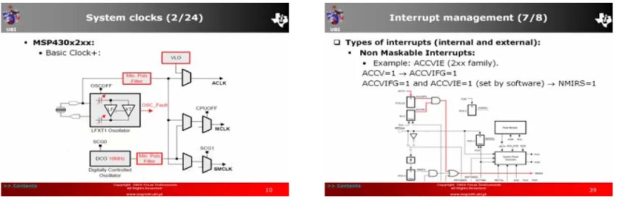
The internal device systems of the MSP430 are described in this section based on the information provided by [1-6]. It includes a description of the internal system reset and clock sources (low/high frequency oscillator - LFXT1; second crystal oscillator - XT2; digitally-controlled oscillator – DCO; frequency locked loop – FLL; and internal clock signals). The MSP430 supports interrupts, that is, events that occur sporadically and need to be processed immediately. The interrupt sources, both external and internal, cause the CPU to suspend execution of the current task, re-direct program flow to an interrupt service routine devoted to the specific event, then resume the former task. How the microcontroller responses to an interrupt may dictate its performance and how the software needs to be written. This section covers all of the above points describing the interrupts management depending on their type (reset; (non)-maskable interrupts (NMI) by Global Interrupt Enable -GIE; maskable interrupts by GIE) and source (internal and external), extending them to the low power operating modes that are one of the main features of the MSP430. This section focuses the internal device systems supported by the MSP430 families that are used with the hardware development tools (2xx and 4xx families). The 16-bit watchdog timer (WDT) module that can be used as a Processor supervisor (supervise the correct operation of the application software) or Interval timer (configured as an independent interval timer, to perform a “standard” periodic interrupt on counter overflow) is also described. The following topic covers the description of the Supervisory Voltage System (SVS) module used to monitor the supply voltage or an external voltage. The section ends with one of the main features of the MSP430 families, which are their low power consumption (around 1 mW/MIPS or less). This is increasingly important with the growth of battery operated embedded systems devices. Although the MSP430 families are designed for low power
consumption, it should borne in mind that this goal can only be accomplished using a design utilizing low power operating modes. The total power consumption depends on several factors: clock frequency, ambient temperature, supply voltage, peripheral selection, input/output usage and memory type. The MSP430 architecture allows six operating modes. Five of these modes are suitable for low power consumption operation. These modes are configured by the Status Register bits. In Figure 1 are shown 2 slides covering different topics exposed during this section.
2.3 General purpose Input/Output
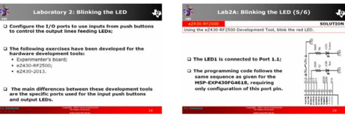
This section starts with a description of one of the simplest integrated peripherals of the MSP430 – the General Purpose 8-bit Input Output (GPIO) [1-3]. The Input/Output (I/O) ports can be configured as interruptible or non-interruptible. Additionally, the port pins can be individually configured for general-purpose use, or as special function I/Os, such as USARTs, comparator signals and ADCs. Following the technical details, there is the first in a series of hands-on laboratories. The laboratory uses the input lines to read the state of push button switches and uses the output lines to feed light emitting diodes (LEDs). The first hands-on laboratory chands-onsists of chands-onfiguring the I/O ports, setting up the input lines to read push buttons and the output lines to feed LEDs. The following exercises have been developed for the three hardware development tools. The first to be discussed is the MSP-EXP430FG4618 Experimenter’s board. Modifications are later made to suit the other development boards. The main differences between the boards are related to the specific ports in which the buttons and LED are (or can be) connected. For the development of this laboratory, Code Composer Essentials v3 has been used. In Figure 2 are shown the slides covering the laboratory statement and part of its solution for the eZ430-RF2500 hardware tool.
Figure 2 – Slides of the laboratory included in the General purpose Input/Output section. 2.4 Timers
Correct system timing is a fundamental requirement for the proper operation of a real-time application. The timing definition can dictate how the data information processed during the execution of the application program. The clock implementations vary between devices in the MSP430 family [1-2]. Each device provides different clock sources, controls and uses. This section discusses the clock controls included in the platforms used. The MSP430 4xx family has two general-purpose 16-bit or 8-bit counters and event timers, named Timer_A, Timer_B, and a Basic Timer. The Basic Timer module is only implemented in 4xx devices. The 2xx device family also has Timer_A and Timer_B, but the clock signals are provided by the basic clock module+. The timers may receive an internal or external clock. Timer_A and Timer_B also include multiple independent capture and compare blocks, with interrupt capabilities. The capture and compare blocks are suited for applications such as timed events and Pulse Width Modulator (PWM) respectively. Timer_A and _B have several operating modes each one with its own characteristics. As the different system clocks sources that allow the CPU and peripherals to operate, depending on the device in the MSP430 family were described, this section will focus mainly on the configuration and operation of timers and their different uses.
The first hands-on laboratory consists of configuring the LCD_A controller of the MSP430FG4618 device of the Experimenter’s board to put a message on the display using the CCE software development tool. The next laboratory implements a memory clock using the features provided by Timer1. The clock is updated once every second by the Basic Timer1 interrupt service routine (ISR). This procedure also performs switching of LED1. In order to evaluate the execution time of the routine, LED2 is kept active during the execution of the ISR. When the ISR has completed, the device goes into low power mode, until the new interrupt wakes it up. The Real Time Clock (RTC) has a 32-bit counter, to automatically control the clock calendar. This peripheral is present on the MSP430FG461x devices. The application developed in the previous
laboratory will now be modified to incorporate this module in an additional laboratory exercise. The following laboratory exercise consists in building a memory clock similar to the one that was developed using the Basic Timer1, but now making use of Timer_A, configuring it to generate an interrupt once every 100 msec. The ISR manages the memory clock. LED1 and LED2 are used to monitor the operation of the system state. The purpose of the next laboratory exercise is to build a sound generator using Timer_B. The pulse-width modulation (PWM) signal produced by this peripheral drives the buzzer, producing a sequence of musical notes at regular time intervals. At the same time, LED1 and LED2 switch state alternately. The volume of sound produced by the buzzer can be controlled by push buttons SW1 and SW2. The hands-on laboratories topic finishes with the development of an application designed to measure a PWM signal frequency. The frequencies generated are acquired (from the signal generator equipment) or read (from a file if the previous equipment isn't available) and updated with a fixed time period using the features of CCE. The measured value is shown on the LCD in Hz.
2.5 LCD Controller
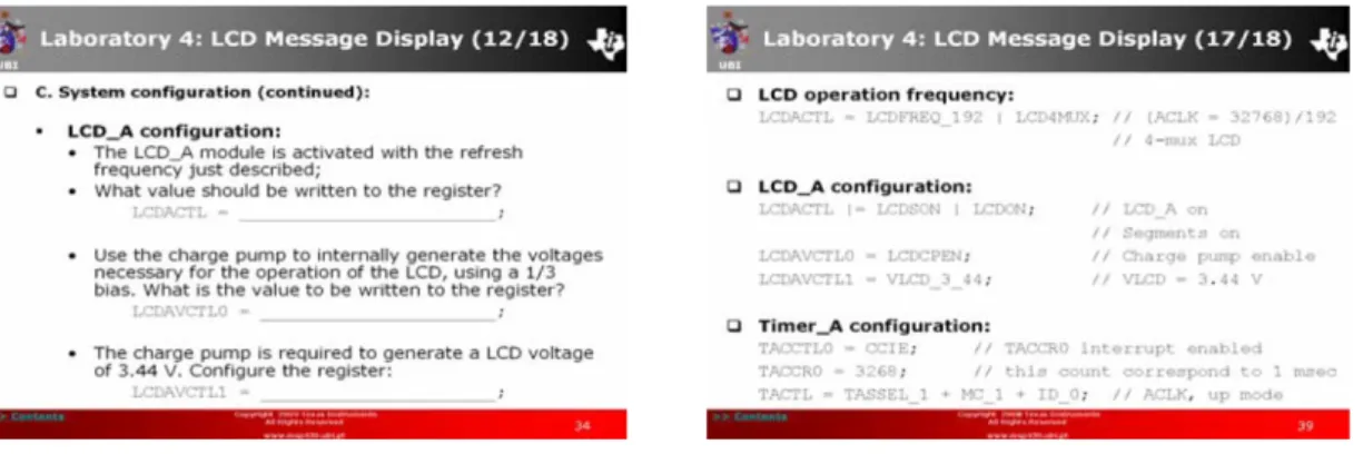
The Liquid Crystal Display (LCD) controller, which is incorporated into several devices in the MSP430 family (’3xx and ’4xx) [2], provides a rapid and simple way to interface between a program and an LCD display. The LCD controller controls the LCD display, generating voltage signals for the segments. It supports static and multiplexed display interfaces (2 mux, 3 mux and 4 mux). This section describes in detail the LCD driver interface and LCD_A controller, both of which are implemented in the MSP430FG4618 device on the Experimenter's board. The hands-on laboratory consists of configuring the LCD_A controller of the MSP430FG4618 device of the Experimenter’s board to display a message on the LCD display. Figure 3 shows the slides covering the laboratory steps to configure the LCD controller as well part of its solution for the experimenter's board hardware tool.
Figure 3 – Slides of the laboratory included in the LCD Controller section.
2.6 Direct Memory Access (DMA)
The MSP430 is well suited to low-power applications, and the Direct Memory Address (DMA) controller is a very useful facility to have in order to achieve this. This module is supported by some devices in the MSP430 family providing the capability to move data from one location to another, without CPU intervention. This increases the throughput of peripheral modules and also allows the CPU to remain in a low-power mode, without needing to wake up to perform the data transfer. This gives the benefit of reduced power consumption. Data transfers to/from peripherals can be initiated by external and internal events, using triggers.
This section covers DMA operation, supported addressing and transfer modes, trigger selection, channel priorities and DMA controller interrupts. It ends with a laboratory exercise, where the data transfer between two regions of memory is analyzed. The order of transfer is controlled by software. The DMA controller is used to automatically transfer data between data memory and the DAC12 data register. A sinusoidal waveform is produced at the output of the DAC, without CPU intervention. The development of this section is based on the MCU user guides [1-2] and on technical books [4-5, 7-8].
2.7 Hardware Multiplier
The MSP430 hardware multiplier is a peripheral device and does not constitute part of the MSP430 CPU. It allows the multiplication of both signed (MPYS) and unsigned (MPY) numbers to be carried out. The multiply and accumulate (MAC) operation is also supported, which is useful for implementing digital signal processing (DSP) tasks such as Finite Impulse Response (FIR) filters. The laboratory exercise explores the hardware multiplier peripheral. It is composed of three different tasks, each of which evaluates a different characteristic of the hardware multiplier peripheral: multiplication operation execution time, with and without the hardware multiplier and the differences
between the use of the operator “*” and direct write to the hardware multiplier registers. The task operational analysis is performed, in which the active power and the RMS value of an electrical system are calculated. The execution times are measured using an oscilloscope. The bibliography references that support this section are the same as the previous one.
2.8 Flash Programming
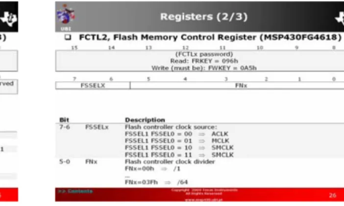
To use the MSP430 in a stand-alone embedded application, the application code needs to be stored in flash memory. The MSP430 flash memory module is bit-, byte-, and word-addressable and programmable, using a controller that supervises the programming and erase operations. The controller has three (or four) registers, a timing generator, and a voltage generator to supply program and erase voltages. This section covers flash memory module operation and segmentation, and finishes with a laboratory exercise. Two different methods of writing to the flash memory are studied in this laboratory. The first method requires the CPU execution of the code resident in flash memory, so whenever a flash write or erase operation occurs, the CPU access to this memory is automatically inhibited. The operation of this device is monitored using a digital output port (P2.1). The consequences of this procedure are discussed. In the second part of the laboratory, the flash write and erase operations are conducted with the CPU executing the code resident in RAM. The important details are highlighted such as special procedures required by the process. The routines to run from RAM must be identified. The application must begin by copying the routines from flash to RAM. The bibliography references supporting this section are the same as the previous one. Figure 4 include slides where the flash memory controller registers bits are exposed.
Figure 4 – Slides of the covered topics in the Flash Programming section.
3. CONCLUSIONS
It was presented the teaching structure in the lectures that use microprocessors at the undergraduate and graduate Electrical related courses at the University of Beira Interior, Portugal that make use of microcontrollers, including signatures such as, Instrumentation and Measurements; Data Acquisition; Automation and Robotics; Industrial Informatics; Real Time Systems; Embedded Systems; Bionic Systems and Monitoring and therapy medical portable devices. The former last five signatures integrate several knowledge that are acquired during the courses.
The first part of this paper presented the outline of the course. Particularly, its structure, and the initial subjects covering an introductory overview in logic design and embedded processors and a description of the available software and hardware development tools for the MSP430. This second part describes the MSP430 Architecture, Device Systems and Operating Modes, General purpose Input/Output and all the peripherals integrated in the MSP430 family devices.
The projects development making use of the microcontroller has proven to be a valuable teaching tool for motivating and stimulating the students, allowing the reinforcement of several key concepts discussed in undergraduate signatures. With this pedagogical approach, the students gain much more experience since they are challenged to develop, not overwhelming, but much more complex projects, while keeping them motivated.
ACKNOWLEDGMENTS
The authors thank the support given by Texas Instruments; and particularly the help provided by Robert Owen (TI University Programme Manager).
REFERENCES
[1] Texas Instruments, MSP430x2xx Family, User’s
Guide. SLAU144E, Texas Instruments, 2008.
[2] Texas Instruments, MSP430x4xx Family, User’s
Guide. SLAU056G, Texas Instruments, 2007.
[3] Texas Instruments, MSP430x5xx Family, User's Guide. SLAU208, Texas Instruments, June 2008.
[4] F. Pereira, Microcontroladores MSP430: Teórica e
prática. 1ª Ed. Editora Érica, São Paulo, Brasil, 2005.
[5] J. Luecke, Analog and digital circuits for electronic
control system applications: Using the TI MSP430 microcontroller. Elsevier, Embedded Technology
Series, 2005.
[6] M. Mitchell, "MSP430F2xx family enhancements and features," SLAP111, in Proc. ATC 2006 – MSP430
Advanced Technical Conference, Texas Instruments,
Sonthofen, Germany, 2006.
[7] C. Nagy, Embedded systems design using the TI
MSP430 series. Elsevier, Embedded Technology
Series, 2003.
[8] J. H. Davies, MSP430 Microcontroller basics. Elsevier Science, Newnes, 2008.