*e-mail: [email protected]
Carbon Based Nanostructures: Diamond
Clusters Structured with Nanotubes
O.A. Shenderova*, D. Areshkin, D.W. Brenner
North Carolina State University, Raleigh - NC 27695, USA
Received: January 02, 2002; Revised: September 30, 2002
Feasibility of designing composites from carbon nanotubes and nanodiamond clusters is dis-cussed based on atomistic simulations. Depending on nanotube size and morphology, some types of open nanotubes can be chemically connected with different facets of diamond clusters. The geometrical relation between different types of nanotubes and different diamond facets for con-struction of mechanically stable composites with all bonds saturated is summarized. Potential applications of the suggested nanostructures are briefly discussed based on the calculations of their electronic properties using environment dependent self-consistent tight-binding approach.
Keywords: carbon, nanostructures, modeling
Another candidate for a basic building block for nanotechnology applications, nanodiamond clusters, can be obtained in a large amount with an exceptional uniformity and reproducibility, for example, by detonation technique4.
The particles extracted from detonation soot are subjected by post-processing chemical modification to remove exter-nal carbon shell. Nanodiamond cluster size ranges between 2-10 nm with a very narrow peak of size distribution at about 4-5 nm4. While information on a shape of nanodiamond
clusters is very scarce, it was demonstrated that diamond particles of a micron dimensions are regularly shaped and may exhibit a variety of morphologies including cubo-oc-tahedron, icosahedron and a decahedral-Wulff-polyhedron5.
Previously we performed calculations of the electronic prop-erties of single nanodiamond clusters as a function of their size, shape, hydrogen termination and presence of the amor-phous ‘coating’ on the particle using an environment de-pendent tight binding Hamiltonian6,7. Particularly, it was
found that size effect for band structure is quite noticeable for cluster sizes less than 2.0 - 3.0 nm, while electrostatic potential distribution is less sensitive to a cluster size. It was also found that effect of cluster shape on band struc-ture is of minor importance. Similar to extended diamond surfaces, hydrogen passivated clusters exhibited negative electron affinity (up to -1.5 eV depending on the surface structure). While surface states decreased band gap of clus-ters by about 1 eV as compared to that of bulk diamond6,
1. Introduction
The emerging field of nanoengineering requires the de-sign of nanoscale structures that have controllable physical and chemical properties, and that can be constructed from readily accessible building blocks such as, for example, nanodiamonds and nanotubes. Nanodiamonds and carbon nanotubes are unique structures that have diverse electronic properties depending on their size and morphology and that can be produced in bulk quantities. The feasibility of de-signing structures composed of nanodiamond clusters and carbon nanotubes as well as some of their electronic prop-erties will be discussed in the paper.
Carbon nanotubes of 1-50 nm in diameter and typically a few microns long can be synthesized by several methods such as laser vaporization, arc discharge, pyrolysis and chemical vapor deposition techniques1. The electronic
struc-ture of a single-wall carbon nanotube is either metallic or semiconducting, depending on its diameter and chirality2.
The energy gap of semiconducting carbon nanotubes can be varied continuously from ~1 eV to ~0 eV, by varying the nanotube diameter. Although not efficient yet for a mass production, a technique using atomic force microscope to manipulate single nanotubes in a controlled way had been developed3. The capability of cutting a nanotube as well as
presence of amorphous carbon ‘coat’ with different sp2-carbon content is the dominant factor of tuning the band gap value up to its full disappearing7.
Thus, the carbon-based building blocks with versatile properties can be considered for design of different nanostructures. An experimental evidence of a nanotube, perpendicularly attached to a diamond surface was reported by Kuznetsov et al.8. The structure was formed during
an-nealing of diamond particles of micron size. Very recent results of simultaneous growth of hybrid structures of dia-mond crystallite and carbon nanotubes at the same substrate by plasma-enhanced CVD process had been reported by Ayres et al. and Avigal et al.9. The structures were not
or-dered, however. In work related to that presented here, sev-eral specific closely matched diamond-fullerene nanotube interface structures have been modeled. Sinnott and coworkers, for example, used atomic simulations to model bonded interfaces between diamond {111} surface planes and (6,0) fullerene nanotubules10. For a sufficiently high
density of bonded nanotubes, these structures are predicted to have elastic moduli comparable to diamond but at a lower overall density. The generalized rules for bonding nanotubules to the surfaces of diamond structures had been discussed in details by Shenderova et al.11. These rules were
derived based on geometrical considerations in combina-tion with energies and stresses estimated from atomic modeling using an analytic potential function. It was con-cluded that a wide array of such structures could be pro-duced that are mechanically and chemically stable.
In the current paper classes of possible nano-diamond/nanotube hybrid structures are summarized. Nanotechnology applications of the suggested composites such as electronic devices and field emitting arrays are briefly discussed.
2. Simulation Techniques
Identifying potentially stable bonding interface struc-tures requires determining sites available for bonding at an edge of an open nanotube and those on a free diamond sur-face such that the maximum number of bonds between the two structural components are formed. To initially define general geometrical trends that fulfill this requirement be-tween different types of carbon nanotubes and (111) and (001) diamond surfaces, the TurboCad® software was used. This software allows various in-plane translations and rota-tions of geometrical objects, and facilitates visual analysis of the possible hybrid structures. Figure 1 illustrates the results of such analysis for zigzag nanotubes and (111) dia-mond surface. After being generated with TurboCad® , all of the structures reported below were relaxed to their mini-mum energy configurations using an analytic many-body bond-order potential energy function for hydrocarbons12 that
mimics bonding in carbon systems for a wide range of atomic hybridizations.
Electronic properties of the relaxed hybrid structures were calculated self-consistently using an environment-de-pendent tight binding model for hydro-carbons6,7. This
model reproduces the bulk diamond band gap and provides qualitative descriptions of the bulk diamond and graphite band structures. Details on the C-H tight binding parameterization are given in references6,7.
3. Nanodiamond/Nanotube Structures:
Geometrical Compatibility
Regularly shaped diamond micro-particles (for exam-ple, cubo-octahedrons) typically exhibit (001) and (111) facets. Recently, diamond nanoparticles of 5 nm in diam-eter with noticeable (111) facets had been also observed13.
Thus, possibilities of bonding of nanotubes with (001) and (111) diamond surfaces are summarized below. The analy-sis is restricted to nanotubes perpendicularly attached to the diamond facets. This restriction requires that the plane of an edge of an open nanotube be perpendicular to the tube axis. Only zigzag and armchair types of nanotubes were considered because all dangling bonds of the nanotube edges are within the same plane, and the bond density is high as compared to chiral nanotubes. The high bond density pre-sumably results in strong bonding for zigzag and armchair nanotubes as compared to chiral structures.
3.1 Bonding between zigzag nanotubes and diamond clusters
A wide variety of zigzag nanotubes can be attached to the (111) diamond surface with all bonds at the interface saturated. According to the pattern of sites available for bonding on the (111) diamond surface, it is possible to con-nect sites in a shape of a polygon with any number of seg-ments N (starting with N = 3) of equal lengths aD=2.52 Å. To obtain chemical bonding between a (n,0) nanotube and the corresponding N-sided polygon formed by dangling bonds on a diamond surface, the shape of the polygon should be as close as possible to circular to mimic that of a nanotube edge. The total mismatch between a nanotube of perimeter
LT and the perimeter of a polygon on the diamond surface
LD would be:
, D T D D T D tot a a a L L L − = − = δ (1)
where the distance between sites available for bonding at the edge of a zigzag tube (n,0) depends on the tube param-eter n as:
n N a a Gr T π π sin 3 = (2)
The parameter aGr= 2.46 Å is a distance between atomic sites at the zigzag edge of graphene. For example, the total mismatch for a (6,0) nanotube is 6.7%, while that for (24,0) nanotube would be only 2.6%. Such strain, and even higher values as shown below, can be easily accommodated by the nanotube because of its high flexibility.
Second to total mismatch, which just reflects the chang-ing of the inter-site distance at a tube edge as the tube cur-vature is changed, the most important feature determining stability is local mismatch. The local mismatch can be de-fined as the distance between a vertex of a polygon on a diamond surface and the point of the projection of a corre-sponding atom from a nanotube edge (Fig. 1). As it can be seen from the Fig. 1, some of the interface bonds are more locally deformed for nanotubes of bigger radius, so indicat-ing higher local mismatch. For (6,0) and (24,0) nanotubes this local mismatch would be 0.17 Å and 0.68 Å, respec-tively. A particular local mismatch can be more easily ac-commodated if a nanotube diameter is large because strain can be redistributed among a larger number of bonds of neighboring atoms. In addition, as discussed above, nanotubes with bigger radii posses less total mismatch with a polygon formed by atomic sites on a diamond surface, so that the interface energy of the relaxed structures is less for nanotubes with larger radii (Table 1).
Six distinct groups of nanotubes with different geometri-cal rules of bond formation had been identified depending on a parameter n of an (n,0) nanotube (Fig. 1). Detailed discussion of bonding rules for these groups of nanostructures is provided in Ref. (11).
Thus, a relatively wide variety of types of nanotubes can be attached to (111) diamond facet due to the low mis-match between sites available for bonding at the (111) sur-face and those at a zigzag tube edge. Another important factor is a high density of surface sites on the (111) dia-mond surface that posses six-fold symmetry and thus every surface atom has six neighbors in a plane. This provides more flexibility for curving a line of attachment of a sheet of graphene to the surface. This line can be deviated from a straight line by 30° or 90° without changing the distance between sites available for bonding. For the (100) diamond surface the situation is less favorable. Due to the four-fold symmetry of the surface sites at a (100) surface, deviation of a line of attachment from a straight line without chang-ing the distance between sites available for bondchang-ing is pos-sible through curving by 90° only. Another pospos-sible devia-tion by 45° is accompanied by changing the inter-site dis-tance by a factor of √2. While this strain can still be accom-modated by a nanotube the interface energy of the struc-tures containing such segments is noticeably higher than for other structures.
After analyzing numerous possibilities for bonding (100) surfaces (both unreconstructed and reconstructed) with dif-ferent types of zigzag nanotubes, it was concluded that it is not possible to develop general schemes for tube attach-ment as in a case of the (111) surface and zigzag nanotubes (Fig. 1). There are a limited number of zigzag nanotubes that can be attached to a (100) diamond surface with all bonds at the interface saturated (by surface reconstruction or through adding hydrogen). Examples of such hybrid structures include (6,0), (8,0), (12,0), (16,0) and (18,0) nanotubes on diamond (100) surface. Relaxed hybrid struc-ture between a (100) facet of truncated octahedron diamond cluster and the (12,0) nanotube is illustrated in Fig. 2. Al-though the interface energies for these nanotubes and the (100) diamond surface are higher those for the nanotubes and the (111) diamond surface, they are still reasonable (Table 1).
3.2 Bonding of armchair nanotubes with diamond clusters
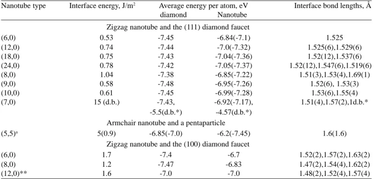
Table1. Energetic characteristics and bond lengths at nanotube/diamond interfaces. Values in parentheses for bond lengths correspond to the number of bonds of the given length at the interface. In the column ‘nanotube’ value in parentheses corresponds to energy per atom in relaxed single nanotube (reference point for the interface energy calculations).
Nanotube type Interface energy, J/m2 Average energy per atom, eV Interface bond lengths, Å
diamond Nanotube
Zigzag nanotube and the (111) diamond faucet
(6,0) 0.53 -7.45 -6.84(-7.1) 1.525
(12,0) 0.74 -7.44 -7.0(-7.32) 1.525(6),1.529(6)
(18,0) 0.75 -7.43 -7.04(-7.36) 1.52(12),1.537(6)
(24,0) 0.78 -7.42 -7.05(-7.37) 1.52(12),1.547(6),1.519(6)
(8,0) 1.04 -7.38 -6.85(-7.22) 1.51(3),1.53(4),1.69(1)
(9,0) 0.58 -7.48 -6.95(-7.26) 1.52(6), 1.53(3)
(10,0) 0.61 -7.45 -6.99(-7.28) 1.53(6),1.55(4)
(7,0) 15 (d.b.) -7.43, -6.92(-7.17), 1.51(4),1.57(2),1d.b.*
-5.5(d.b.*) -4.57(d.b.*) Armchair nanotube and a pentaparticle
(5,5)a 5(0.9) -6.85(-7.0) -6.2(-7.45) 1.6(1.6)
Zigzag nanotube and the (100) diamond faucet
(6,0) 1.7 -7.4 -6.7 1.52(2),1.57(2),1.63(2)
(8,0) 1.2 -7.47 -6.83 1.47(2),1.54(4),1.62(2)
(12,0)** 1.6 -7.0 -7.0 1.48(2),1.52(4),1.57(4)
d.b.* - dangling bond.
** - (12,0) nanotube was attached to the dimerized diamond surface (Fig. 2).
a- values in parenthesis correspond to a structure with hydrogen atoms attached to the (5,5) nanotube atoms near the interface to decrease the energy.
Figure 2. Illustration of the relaxed hybrid structure between a diamond truncated octahedron cluster and the (12,0) nanotube. The nanotube is attached to the (100) facet of the cluster.
boundaries and an axis of symmetry oriedegreesnted along the <110> direction. Diamond pentaparticles have been ob-served experimentally as free standing structures resulting from vapor phase growth14 as well as five-fold microcrystals
embedded in chemical vapor deposited diamond films15.
Sites available for bonding at the intersection of twin boundaries with a surface are only about 1.55 Å away from each other. The distance between other sites available for bonding on (111) diamond surfaces is about 2.54 Å. Thus a pattern of sites available for bonding on a surface of a pentaparticle mimics that at an edge of the armchair (5,5) nanotube. The total mismatch is about -4.1%. Energetic characteristics of the interface are summarized in Table 1. A relaxed hybrid structures constructed from (5,5) nanotubes and penta-particles are illustrated in Fig. 3.
4. Potential applications of hybrid structures
single-wall and multisingle-wall carbon nanotubes have demonstrated satisfactory current at relatively low operation voltage16.
Moreover, flat panel displays fabricated with aligned bun-dles of carbon nanotubes as emitters have been also dem-onstrated16. According to the present tight binding
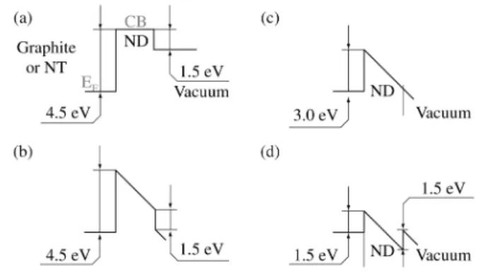
simulations, the work functions of a single closed nanotube and a single nanotube with an edge terminated by hydrogen are about 4.5-5 eV. The barrier at the back contact of the diamond cluster/metallic nanotube varies from 4.5 to 2-3 eV depending if a nanodiamond cluster consists of pure dia-mond phase (Fig. 4a, b) or contains tetrahedrally coordi-nated (ta-C) carbon phase (Fig. 4b, c). Taking into account the negative electron affinity at the hydrogenated surface of a diamond cluster6,7, resulting emission barrier for the
hy-brid structure is comparable or lower then that for a single nanotube. Calculations also indicate the presence of the wave functions with energies near Fermi level which are continu-ously extended along both nanotube and diamond cluster. This enhances possibility of current flow from the nanotube to a diamond cluster. Probably, the major advantage of the above design of a nanotube capped with a nanodiamond particle may be reducing of tube erosion resulting in in-creased device lifetime. Indeed, during emission from a sin-gle nanotube current density at the emission sites at the nanotube end is relatively high while for a structure capped with a nanodiamond there are more emitting sites available resulting in less current density. In addition, hydrogenated diamond surface is more mechanically stable then strength of bonding of atoms at the nanotube end. Extended results
on the emission properties of the hybrid structures will be published elsewhere7.
Of particular interest for nano-lithography applications is fabrication of arrays of electron guns using carbon-based materials17. Nanotubes perpendicularly attached to a
sur-face of diamond film might be candidate structures with good bonding between components, assuming that electron supply into substrate is provided. The above analysis se-lects candidate nanotubes which can be attached to a par-ticular low-index diamond surface.
One of the current carbon nanotubes applications is proximal probe tips. They are either formed as by gluing the nanotube to the Si cantilever or by growing them at the cantilever directly through a CVD process. A nanotube form-ing strong chemical bonds with a diamond cantilever can be a good candidate for a proximal probe tip.
Finally, the hybrid structure consisting of a short nanotube sandwiched between two diamond clusters (Fig. 5a), mimic a double barrier structure of the resonant tunneling diode18. Because of the finite tube length, the
en-ergy of the confined electron level in a short nanotube is higher then the Fermi level of the conducting nanotubes which can be attached to the external facets of the diamond clusters to form a circuit. More over, the energy of the con-fined electron level can be varied through variation of nanotube length and morphology (Fig. 5b). These results are consistent with those by Rochefort et al.19 obtained with
ab-initio and semiempirical quantum computational tech-niques. The present tight binding simulations also demon-strate the penetration of the nanotube wafe function into the diamond cluster, what ensures the finite probability for electron tunneling through the cluster to the confined level
Figure 4. Homogeneous Emission through nanodiamond cluster. Band structure for graphite/diamond/vacuum when (a) no field is applied and (b) under applied field. The difference between Fermi level and CB edge depends on geometry and may vary between 5.5 eV and 3.0 eV. CB edge position in tetrahedrally coordinated a-C depends on amorphization degree. Band structures in applied field for a-C with zero (c) and positive (d) EA.
at particular applied voltage.
While developing hypothetical structures for nanotechnology applications, it is always important if fab-rication of these structures is practically accessible. The hybrid structures discussed above can, in principle, be syn-thesized by manipulating of diamond clusters with a proxi-mal probe tip with a nanotube mounted at the end of the tip. While this way of assembling of nanoscale building blocks would be a powerful tool to test a concept, however it is not suitable for the mass production.
One of the more practical ways for fabrication of the suggested hybrid structures might be
electrophoresis/dielec-trophoresis techniques, involving directional movement of charged/polarized particles in the suspensions under nonuniform electric field. These techniques had been suc-cessfully used for deposition of nanodiamond powder on arrays of silicon tips for cold cathode fabrication20. Similar
to this, a deposition of nanodiamond powder on the arrays of carbon nanotubes can be considered. The growth of nanotube arrays oriented perpendicular to a substrate had been demonstrated earlier, for example, by Dai et al.21.
Simi-larly, it can be expected that in a suspension of nanodiamond particles and open nanotubes in organic liquids, under ap-plied electric field there will be dipoles formation along carbon nanotubes which will interact with charged diamond particles and form hybrid structures.
5. Conclusion
It had been demonstrated, that depending on a nanotubes morphology, some types of open nanotubes can be chemi-cally connected with different diamond surfaces, atom to atom. Structures without dangling bonds at the interface can be formed, what is important for the nanoelectronics applications, because dangling bonds at the interface can trap electrons and suppress conductivity through the inter-face. Thus combining metallic or semiconducting nanotubes with diamond clusters or substrates, different types of heterojunctions can be designed for the carbon-based nanoelectronics applications.
The results of atomistic simulation also indicate that sig-nificant lattice mismatches between a diamond surface and a nanotube can be accomodated by a nanotube due to its high flexibility. Thus, in principle, chemically bonded hy-brid structures between selected nanotubes and silicon car-bide surface can be also considered.
Results of the present study are also related to the con-cept of molecular manufacturing using carbon-based struc-tures22.
Acknowledgments
The financial support of the Office of Naval Research, NASA-Ames, and the National Science Foundation is grate-fully acknowledged. Drs. V. Zhirnov and A.Kvit are thanked for helpful discussions.
References
1. Science and Application of Nanotubes, edited by D.Tomanek and R.J.Enbody, Kluwer Academic/Plenum Publishers, New York, 2000.
2. Dresselhaus, M.S.; Dresselhaus, G.; Eklund, P.C.
Sci-ence of Fullerenes and Carbon Nanotubulus, Academic
Press, San Diego, 1996.
3. Avouris, P.; Hertel, T.; Martel, R.; Schmidt, T.; Shea, H.R.;
Walkup, R.E. Appl. Surf. Sci., v. 141, p. 201, 1999. 4. Kuznetsov, V.L.; Chuvilin, A.L.; Butenko, Y.V.; Malkov,
I.Y.; Titov, V.M. Chem. Phys. Lett., v. 222, p. 343, 1994 and references there in.
5. Diamond Films and Coatings, ed. by R.Davis, Noyes Publ., New Jersey, USA, 1992.
6. Areshkin, D.A.; Shenderova, O.A.; Zhirnov, V.V.; Pal, A.F.; Hren, J.J.; Brenner, D.W. MRS Symp.Proc., v. 621, ed. by K.L. Jensen et al., 2000.
7. Areshkin, D.A.; Shenderova, O.A.; Brenner, D.W. sub-mitted to Phys.Rev. B.
8. Kuznetsov, V.L.; Chuvilin, A.L.; Butenko Y.V. et al.
Chem.Phys.Letters, v. 289, p. 353, 1998; Kuznetsov, V.L.;
Zilberberg, I.L.; Butenko, Y.V.; Chuvilin, A.L.; Segall, B. J.Appl.Phys. v. 86, p. 863, 1999.
9. Ayres, V.; Wright, B.; Asmussen, J.; Song, S. et al.
Electrochem.Soc.Proc., v. 2000-12, Edited by P.Kamat,
D.Guldi, K.Kadish, p. 236; Y.Avigal, R.Kalish, Abstract book, 12th European Conference on
Diamond,Diamond-like materials, Carbon nanotubes, Nitrides & Silicon Carbides, Budapesht, Hungary, September, 2001. 10. Sinnott, S.B.; Shenderova, O.A.; White, C.T.; Brenner,
D.W. Carbon, n. 36, p. 1, 1997.
11. Shenderova, O.A.;.Areshkin, D.A.; Brenner, D.W.
Molec. Simul., in press.
12. The original potential is discussed in D.W. Brenner, Phys.
Rev., B 42, p. 9458, 1990.
13. Taylor, A.; Kwit, A.; Zhirnov, V. private communica-tion.
14. Matsumoto, S.; Matsui, Y. J. Mat. Sci., v. 18, p. 1785, 1983.
15. ‘Diamond Films and Coatings’, ed. by R.Davis, Noyes
Publ., New Jersey, USA, 1992.
16. Choi, W.B.; Chung, D.S.; Kang, J.H.; Kim H.Y. et al.,
Appl.Phys.Lett., v. 75, n. 3129, 1999.
17. Teo, K.B.K.; Yuan, J. http://www2.eng.cam.ac.uk/ ~www-edm/projects/nano/1.htm
18. Jaros, M. Physics and Applications of Semiconductor
Microstructures, Clarendon Press, Oxford, 1989.
19. Rochefort, A.; Salahub, D.R.; Avouris, A. J. Phys.
Chem.,v.103, p. 641, 1999.
20. Alimova, A.N.; Chubun, N.N.; Belobrov, P.I.; Detkov, P.Y.; Zhirnov, V.V. J. Vac. Sci. Technol., v. B 17, p. 715, 1999.
21. Dai, H.; Kong, J.; Zhou, C.; Franklin, N.; Tombler, T. et
al. J. Phys. Chem., v. B 103, p. 11246, 1999.
22. Merlkle, R. Chapter 2 in Prospects in Nanotechnology:
Toward Molecular Manufacturing. Edited by M.