DOI: 10.13164/re.2016.0312 CIRCUITS
A Low-Dropout Voltage Regulator
with a Fractional-Order Control
Libor KADLCIK, Pavel HORSKY
ON Design Czech, Vídeňská 125, 619 00 Brno, Czech Republic
[email protected], [email protected]
Manuscript received May 27, 2015
Abstract. This paper presents a 5 V / 50 mA low-dropout voltage regulator (LDO). The LDO uses a fractional-order control for its regulation loop to achieve a high DC gain (for a tight DC regulation) while avoiding (for a good stability) a high gain at high frequency. No compensation zeros are needed. The unity gain frequency of the regula-tion loop also changes adaptively with the output current to maintain it below the frequency of non-dominant poles. The LDO is stable with any external capacitance larger than 50 nF, and is expected to operate in a harsh automo-tive environment, with junction temperature ranging from –40°C to 170°C and with supply voltage from 7 V to 36 V. The operation of the LDO has been verified by realizing it in the 350 nm I3T50 ON Semiconductor technology.
Keywords
Fractional-order control, error amplifier, RC ladder, low-dropout regulator, frequency compensation
1.
Introduction
This section presents classical LDO concepts and their trade-offs of DC regulation error and regulation loop stability, and how the fractional-order control solves them.
1.1
Classical LDO Concepts
A low-dropout voltage regulator is a linear voltage regulator which can maintain a nearly constant output volt-age even if the supply (input) voltvolt-age is very close to the output voltage. LDOs are the most popular class of linear voltage regulators [1], [2], [3], [4], [5], [6].
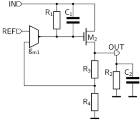
The principal LDO topology is shown in Fig. 1. The transconductor gm1 monitors the output (the pin OUT)
voltage via the resistive voltage divider R3-R4 and controls
the gate of the end stage transistor M2 to set the current
delivered to the output from the input (the pin IN) in order to maintain the output voltage at the desired value (according to the reference voltage at the REF pin). The resulting regulation loop is negative, with two poles: the internal pole (formed by the RC circuit R1-C1) and the
Fig. 1. Principal LDO topology.
external pole (formed by the load capacitance C2 with the
parallel combination of the load resistance R2, the
re-sistance of the voltage divider R3-R4 and the dynamic
output resistance of the transistor M2).
In general, there are three LDO concepts, depending on which poles are dominant and which are non-dominant. Dominant poles set the UGF (unity gain frequency) of the regulation loop, while the non-dominant poles do so in a minor way only and their frequency is preferably above the UGF.
The first concept has both the internal and the exter-nal pole dominant – the open-loop gain of the regulation loop attains the slope of –40 dB/dec. Acceptable stability of the regulation loop requires a compensation zero (with a frequency below or near the UGF) to reduce the slope. An advantage is that the internal dominant pole implies a (nearly) integrative regulation, resulting in a very low DC regulation error.
The third concept makes the internal pole dominant and the external pole non-dominant. Making the external pole non-dominant entails pushing it to a high frequency, (this concept is suitable for the end stage transistor M2
being a voltage follower) and possibly placing an upper bound on the load capacitance C2. An advantage is a very
low DC regulation error.
The first concept enjoys a large popularity because of a low DC regulation error, with many methods for creating the compensation zero described in the literature. In Fig. 4 of [1], the zero is formed by the current-controlled current source. In Fig. 1 of [2], the zero is created by the ESR of the external capacitor and by the capacitor Cf2. In Fig. 5 of
[3], the zero results from a parallel signal path formed by the current amplifier and the capacitor Cf; in [4], the
paral-lel signal path results from the connection of the CFA to the output of the LDO; in [5], the parallel signal path passes through the capacitor Cc. In Fig. 5 of [6], the
com-pensation zero of the output buffer is created by the ESR of the internal on-chip output capacitor.
This paper focuses on the LDO topology in Fig. 2, which is suitable for the first and the second concept. The topology is composed of the end stage current mirror M1-M2, driven by the controller, which consists of the
voltage divider R1-R2 and the transconductor (an error
amplifier with the transconductance Ge(s)).
The regulation loop should have a high DC gain for a tight DC regulation and its UGF should not be too high in order to prevent parasitic poles (or possibly zeros) from affecting its stability. One parasitic pole, pm, is formed by
the transconductance of the transistor M1 with the gate
ca-pacitance Cpm of the end stage mirror. A parasitic zero can
be the zero resulting from the ESR (RESRext) of the external
capacitor Cext. The external dominant pole pout, created at
the output (OUT) by the external capacitance Cext,
in-creases the slope of the open-loop gain of the regulation loop at most by –20 dB/dec.
It should be noted that the term “output current” IOUT(s) implies only the current drawn from the output pin
(OUT), while “load current” Iload(s) also includes the
cur-rent sourced by the external capacitor Cext.
There are several approaches for choosing the transfer function Gc(s) of the controller.
The first approach implements the first LDO concept, making the controller a first-order integrator. An advantage is a very low DC regulation error. The open-loop gain of the regulation loop (VFB – “voltage feedback”) reaches the slope of –40 dB/dec., as shown by the characteristic (a) in Fig. 3. A disadvantage is that stability of the regulation loop requires a compensation zero zcomp to reduce the slope
around its UGF.
The second approach implements the second LDO concept by making the controller a proportional system (with a frequency-independent transconductance at fre-quencies below andnear the UGF). The regulation loop has
Fig. 2. LDO topology with an external dominant pole.
Fig. 3. Open-loop voltage gain of the regulation loop of an LDO with an external dominant pole: (a) – internal pole is dominant, (b) – internal pole is non-dominant, (c) – fractional-order control.
a single dominant pole (pout); other poles (e.g. pm) are
non-dominant and should be, as shown by the characteristic (b) in Fig. 3, above the UGF to prevent them from degrading the stability of the regulation loop. A disadvantage is that a tight DC regulation implies a high UGF, making a good stability difficult to achieve.
With the approaches above, a low DC regulation error entails a high UGF or a compensation zero.
1.2
Proposed LDO Approach
We propose a third approach to choosing the transfer function of the controller of the LDO topology in Fig. 2. This approach is between the first and the second one.
The controller in the first approach can be seen as a “zero-order” voltage-to-current integrator with a transfer function of (where GC0 is its transconductance)
0 C0 C(s) G s
G (1)
while in the second approach it is a first-order integrator with a transfer function of (GCI is the integrator gain)
. )
( CI 1 C
G s
s
We propose the controller being an integrator with the order of 0.5 (a so-called fractional order), as given by the characteristic (c) in Fig. 3 and by the transfer function
5 . 0 CF C( )
G s
s
G (3)
where GCF is the integrator gain. Such a controller has
a gain with the slope of –10 dB/dec. and the phase of –45°. With the external capacitance contributing the slope of at most –20 dB/dec., the magnitude of the gain of the regula-tion loop has a slope of at most –30 dB/dec. The largest phase shift is –135° (there are no right-hand zeros), leaving at least 45° as a phase margin.
Advantages of this approach are high DC gain (a tight DC voltage regulation) and not too high UGF (ensuring a good stability of the regulation loop). Another advantage is that no compensation zero is needed. The external ca-pacitance has a specified minimum, but the maximum is unlimited (while its ESR and ESL are limited).
The pole pm of the end stage mirror should have
a frequency above the UGF to prevent it from degrading the phase margin of the regulation loop.
The response of an LDO with a fractional-order con-trol to a step change of the load current is given by the Mittag-Leffler function [7] and can be described as an ex-ponential decay with an elongated settling (as if its time constant increased with time). A general introduction to a fractional-order control can be found in [7] or [8].
2.
Fractional-Order Impedance
This section describes how to approximate a frac-tional-order impedance, which defines the frequency char-acteristic of the error amplifier of the controller.
An impedance Z(s) = ZFs-α with a positive gain ZF and
a fractional order α between 0 and 1 can be approximated with an infinite RC ladder shown in Fig. 4 [9], [10].
The impedance of the infinite RC ladder is [9]
k
k k
k k
sC R s
Z s
Z
1 1 1
) ( 1 1 )
( frac
(4)
where Zk(s) is the impedance of the k-th series RC circuit. The resistances Rk and capacitances Ck form separate decreasing geometric series [9], [10]
. 1 0
,
, 1 0
,
C 0
k C
R 0
k R
q C
q C
q R
q R
k
k (5)
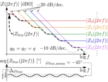
The operation of the infinite RC ladder is explained by Fig. 5. Assume the common ratios qR and qC are
identi-cal (qR = qC = q); the cutoff frequency of the k-th series RC
circuit is proportional to (1/qk)2, while its impedance at its cutoff frequency is proportional to 1/qk [9]. As a result, the
Fig. 4. Infinite RC ladder approximating a fractional-order impedance.
Fig. 5. Explanation of approximating a fractional-order impedance with the infinite RC ladder.
magnitude of the impedance Zfrac(s) of the infinite RC
ladder attains on average half the slope, i.e. –10 dB/dec.
The phase of the frequency characteristic of the im-pedance Zfrac(s) oscillates with the ripple of Δφfrac around
the phase φfrac,mean of the impedance ZFs-α being
approxi-mated; the similar applies to the magnitude. Choosing the common ratios qR and qC closer to 1 reduces the ripple.
The ratio log(qR)/log(qC) sets the order α of the impedance
being approximated.
Only the series RC circuit whose cutoff frequency is near some frequency contributes to the fractional-order behavior at this frequency, as shown in Fig. 5 of [9].
The infinite RC ladder cannot be realized in practice, but can be divided into the following three sections. The middle section approximates the fractional-order imped-ance in the frequency band of interest, while the left and
the right sections “terminate” the RC ladder. This allows reducing the infinite RC ladder to the bilaterally terminated finite RC ladder shown in Fig. 6.
The left section is approximated by a left-terminating resistance RL, given by evaluating a geometric series [9] (as
the left section is assumed to behave mostly resistively in the frequency band of interest)
. 1 1 1
1 1 1
1
R 0 0 0
R R
0 0 R R 1
0 R L
q R
R q q
R q q R q R
k k
k k k
k
(6)
Similarly, the right section is assumed to behave mostly capacitively and is approximated by a right-terminating capacitance of [9]
. 1 C
C 0 0
C 0 C k C 0 R
q q C q C q q C C
n
k k n
n
k
(7)
Without the terminating resistance and capacitance, the frequency range where the bilaterally-terminated RC ladder exhibits an acceptable fractional-order behavior would be narrower [9]. The term “termination” is a loose analogy to a termination of a transmission line (to stabilize its frequency response). The bilaterally-terminated finite RC ladder achieves the frequency characteristic sketched by the characteristic (b) in Fig. 7.
Here, a left-terminated finite RC ladder from Fig. 8 is used instead of the bilaterally-terminated one. The role of the right-terminating capacitance CR is filled by parasitic
poles of the LDO, and an additional phase margin of the regulation loop is gained. Without any parasitic poles, the left-terminated RC ladder has the frequency characteristic (c) sketched in Fig. 7.
Section 5 of [9] demonstrates the RC ladder is largely insensitive to individual (mismatch) component variation; simultaneous variation (process spread) causes only scaling of its impedance without affecting the order α.
Fig. 7. Comparison of the impedances Zfrac(s) of the described
RC ladders: (a) – infinite, (b) – bilaterally-terminated, (c) – left-terminated.
Fig. 8. Left-terminated finite RC ladder approximating a fractional-order impedance.
3.
Fractional-Order Control
The fractional-order behavior of the proposed LDO resides in the error amplifier, whose schematic is in Fig. 9. The error amplifier senses the output voltage via the feed-back resistive voltage divider. The difference between the actual and the target voltage manifests as the current IFB,
causing the action voltage VACT to be adjusted accordingly.
The error amplifier behaves like a transimpedance ampli-fier, whose transimpedance
) (
) ( )
(
FB ACT e
s I
s V s
Z (9)
approximates a fractional-order transimpedance.
The transimpedance of the error amplifier is set mostly by the RC ladder (of the left-terminated finite type), since the transconductance of the OTA (operational trans-
conductance amplifier) exceeds the admittance of the RC ladder. The exception is very high frequencies, where the parasitic poles of the OTA dominate.
The T-circuit R1L0-R1L1-R1L2 has a transconductance
(from the ACT output to the FB input of the OTA) identi-cal to an equivalent left-terminating resistance of
MΩ 084 . 6 FLW 1L2 1L1 1L0 1L1 1L0
10L
R R R R R R
R . (10)
The T-circuit replaces a resistor with such a large re-sistance, reducing the occupied chip area. The virtual ground for the T-circuit is provided by the voltage follower FLW100, which has the nominal output DC resistance RFLW
of 10.38 kΩ (a value that can be met even by a follower-connected single-stage amplifier).
The error amplifier has a low sensitivity to the voltage offset of the follower, since the sum of the resistances of the resistors R1L0 and R1L2 surpasses the output resistance
of the voltage divider of the LDO.
For the design of the RC ladder, we have chosen its impedance Zfrac(s) to approach the order of α = 0.5 with the
phase ripple of Δφfrac = 2.5° (a compromise between too
long ladder and a worst-case degradation of the phase margin of the regulation loop). Using (20) from [9], the phase ripple sets the product of the common ratios of
. 0686 . 0 5 . 2 1 24 . 0 1 24 . 0 C
Rq
q (11)
The product is broken into the individual components [9]
, 262 . 0 10
10 log ( ) 0.5log (0.0686) R
10 C
R
10
q q
q (12)
. 262 . 0 262 . 0 0686 . 0 R C R
C
q q q
q (13)
The equivalent left-terminating resistance R10L is designed
along with the DC transconductance Gv0 of the voltage
divider by (16) and (17), where ZeF is given by a simulation
of the RC ladder. Utilizing (6), the resistance R100 of the
first series RC circuit is calculated from R10L as
2.158M
1 262 . 0 1 10 084 . 6 1 1 6 R L 10 100 q R
R (14)
while its capacitance C100 is chosen to occupy the same
layout area as the resistance R100 (a combination achieving
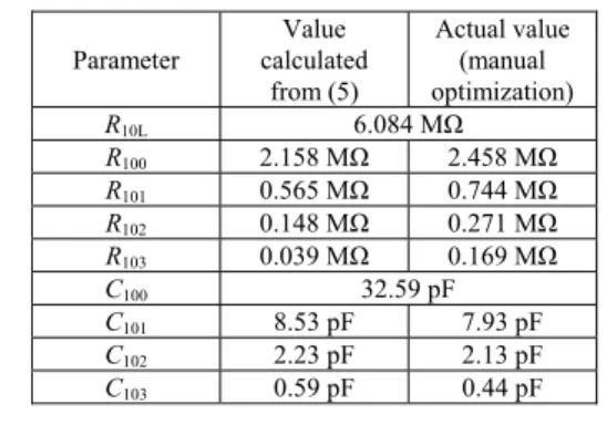
the lowest layout area, given the same cutoff frequency). The other resistances and capacitances are calculated from (5) and summarized in Tab. 1.
The actual values of the resistors and the capacitors of the RC ladder were, as Tab. 1 documents, optimized manually according to simulation results to account for their paraistic capacitances and to compensate for the effect of distant parasitic poles of the LDO.
Parameter Value calculated from (5) Actual value (manual optimization)
R10L 6.084 MΩ
R100 2.158 MΩ 2.458 MΩ
R101 0.565 MΩ 0.744 MΩ
R102 0.148 MΩ 0.271 MΩ
R103 0.039 MΩ 0.169 MΩ
C100 32.59 pF
C101 8.53 pF 7.93 pF
C102 2.23 pF 2.13 pF
C103 0.59 pF 0.44 pF
Tab. 1. Typical component values of the RC ladder of the error amplifier – a comparison of the calculated values and the actual values obtained by manual optimization.
Despite having large values, the components of the RC ladder can be realized well in an analog CMOS (com-plemenatry MOS) technology: capacitors as a MOS struc-ture, resistors as an unsilicided polysilicon strip.
An example of a use and a different implementation of a fractional-order control can be found in [11].
4.
LDO Description
The fractional-order error amplifier has been utilized in an LDO, whose schematic is in Fig. 10. The LDO con-sists of the controller, whose output driving current IDRV(s)
is amplified by the end stage mirror into the output current IOUT(s). In the controller itself, the driving current IDRV(s) is
generated by the driving stage, which is controlled by the action voltage VACT(s), outputted by the error amplifier,
that monitors the output voltage of the LDO via the voltage divider. The error amplifier and other low-voltage blocks are supplied from the low-voltage supply, VDD (voltage VDD), provided by another on-chip voltage regulator.
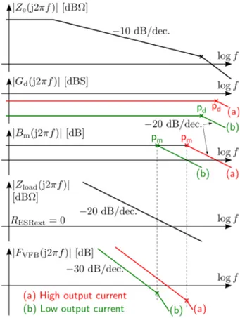
The small-signal AC model of the regulation loop of the LDO is shown in Fig. 11. The magnitude frequency characteristics of the blocks of the LDO are in Fig. 12. The transimpedance Ze(s) of the error amplifier resembles the
impedance of the bilaterally-terminated RC ladder de-scribed in Sec. 2.
The open-loop voltage gain of the regulation loop is
). ( ) ( ) ( ) ( ) ( )
( v e d m load
VFB s G s Z s G s B s Z s
F (15)
Both the end stage mirror (current gain Bm(s)) and
the driving stage (transconductance Gd(s)) have at least one
parasitic pole, as shown by the small-signal AC model of the regulation loop in Fig. 11 and by Fig. 12. The parasitic poles move to lower frequencies with the decreasing output current of the LDO. The cause is a reduction of transcon-ductances of the respective transistors due to lower drain currents, while their parasitic capacitances remain nearly the same.
To keep the frequencies of the parasitic poles above the UGF of the regulation loop in order to prevent them from reducing its phase margin, the transconductance Gd(s)
of the driving stage decreases automatically with the de-creasing output current of the LDO. This ensures the UGF decreases as well, preserving its distance from frequencies of the parasitic poles. We call this process the adaptive UGF adjustment.
With the impedance Zload(s) of the load, the regulation
loop has the gain FVFB(s) with a slope at most -30 dB/dec.
above its UGF, resulting in a phase margin of at least 45°.
Key parameters of the blocks of the LDO are summa-rized in Tab. 2.
Fig. 11. Small-signal AC model of the regulation (VFB) loop of the presented LDO.
Parameter Typical value for
Iload = 50 mA
Name Symbol DC transconductance of
the voltage divider Gv0 8.918 μS
DC transimpedance of
the error amplifier Ze0 R10L = 6.084 MΩ
Gain of the transimpedance of
the error amplifier ZeF 252.2 MΩ·Hz1/2
DC transconductance of
the driving stage Gd0 1.635 mS
DC current gain of the end
stage mirror Bm0 206.5
Tab. 2. Key parameters of the blocks of the proposed LDO.
Fig. 12. Magnitude frequency characteristics of the blocks of the presented LDO.
Using the parameters in Tab. 2, the DC dynamic out-put resistance rOUT and the UGF of the regulation loop with
the external capacitance Cext of 50 nF are calculated as
(both are typical values for 50 mA load current)
, m 6 . 54 1
m0 d0 e0 v0
OUT
B G Z G
r (16)
MHz. 976 . 0 2
1
UGF 2
3
ext m0 d0 eF
v0
C B G Z G
(17)
For comparison, the single-pole models in Fig. 11 of the driving stage and of the end stage mirror have cutoff fre-quencies of 125.6 MHz and 26.1 MHz, respectively.
5.
Simulation Results
The operation of the presented LDO has been verified by simulations of the designed circuit in the ON Semicon-ductor I3T50 technology (350 nm smart power technology) across the corners listed in Tab. 3, i.e. combinations of extremes of the operating conditions and the process spreads of the components (“slow” means a low transcon-ductance, a low gate capacitance and a high threshold volt-age of MOS transistors, while “fast” means the opposite). Each simulation has a nominal run, which sets typical pro-cess parameters and operating conditions (VIN = 8 V,
VDD = 3.3 V, Iload = 50 mA, Cext = 50 nF, zero ESR and
Swept parameter Freq. char. of the reg. loop
DC load
characteristic Step response NMOS, capacitor slow, fast slow, fast slow, fast
PMOS slow, fast slow, fast slow, fast Resistor min, max min, max min, max Input voltage VIN 7 V, 36 V 7 V, 36 V 7 V, 36 V
Low-voltage supply VDD
3.0 V 3.0 V, 3.6 V 3.0 V
Load current Iload
0, 1 mA,
50 mA - -
Ext. capacitance Cext 50 nF - 50 nF
(ESR of Cext,
ESL of Cext)
(0 Ω, 0 nH),
(0.7 Ω, 5 nH) -
(0 Ω, 0 nH), (0.7 Ω, 5 nH) Temperature –50°C, 200°C –50°C, 200°C –50°C, 200°C
Tab. 3. Corners (combinations of operating conditions and process spreads) for simulations of the presented LDO.
line, the low-temperature runs use thin solid lines of cold (blue) colors and the high-temperature runs use thin dashed lines of warm (red, orange and yellow) colors.
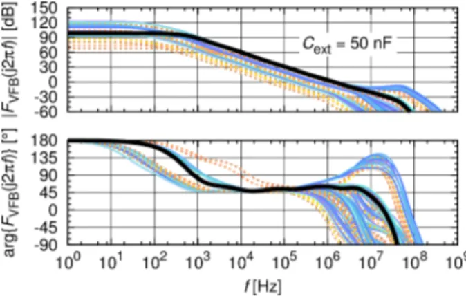
The open-loop voltage gain, plotted in Fig. 13, of the regulation (VFB) loop of the LDO demonstrates the frac-tional-order behavior, since there is a wide region with the phase of 45°. At low frequencies, the phase increases due to the left termination of the RC ladder and due to the ex-ternal pole having a little effect there. At high frequencies, the phase increases (due to the ESR and the ESL) or de-creases (due to parasitic poles). The UGF varies highly due to the adaptive UGF adjustment.
Fig. 13. Simulated open-loop voltage gain of the regulation (VFB) loop of the presented LDO.
Fig. 14. Simulated DC load characteristic of the presented LDO.
The DC load characteristic, plotted in Fig. 14, shows a very tight DC regulation (a low dynamic output re-sistance) of the LDO – a benefit of the error amplifier be-ing a (fractional-order) integrator. The characteristic is convex (having a larger dynamic output resistance at low output currents) because of the adaptive UGF adjustment.
If component mismatch is included (by a mismatch Monte-Carlo analysis or a sensitivity analysis), the output voltage ranges from 4.936 V to 5.073 V (6 sigma interval) across zero to full (50 mA) load current.
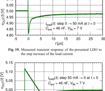
The response of the LDO to the step increase of the load current from 0 mA to 50 mA is plotted in Fig. 15; the response to the step decrease of the load current from 50 mA to 0 mA in Fig. 16 (the triangular portion is caused by the external capacitor being first charged by the over-shoot of the output voltage and then gradually discharged by the load current; the LDO cannot sink any considerable current from its output). The settling part of the responses (excluding the triangular portion) is nearly monotonous, suggesting a sufficient phase margin of the regulation loop, and the shapes agree with the Mittag-Leffler function (i.e. their initially fast decay is more prolonged than it would be for an exponential function).
Fig. 15. Simulated transient response of the presented LDO to the step increase of the load current.
6.
Measurements
The presented LDO has been realized as a functional block in a complex mixed-signal application-specific inte-grated circuit. The layout of the LDO is shown in Fig. 17.
The measurements have been performed at a room temperature on a sample whose process parameters are close to being typical. The input voltage VIN is set to 7 V to
reduce self-heating, but to still guarantee a correct opera-tion of the LDO. The output voltage (VOUT, vOUT) was
measured directly on the bond pads (GND, OUT) to elimi-nate a voltage drop on leads and bond wires.
The measured DC load characteristic of the LDO is shown in Fig. 18. The measured characteristic has a larger
Fig. 17. Layout of the presented LDO.
Fig. 18. Measured DC load characteristic of the presented LDO.
Fig. 19. Measured transient response of the presented LDO to the step increase of the load current.
Fig. 20. Measured transient response of the presented LDO to the step decrease of the load current.
slope than the simulated one in Fig. 14. This is caused by an internal ground shift, whose effect is not eliminated even by a measurement on bond pads and which is not accounted for in the simulation. The measured dynamic output resistance is around 300 mΩ.
The response to the step increase of the load current from 0 mA to 50 mA, captured in Fig. 19, shows a voltage drop of less than 200 mV, which settles mostly in around 10 μs. The step decrease from 50 mA to 0 mA causes a peak lower than 150 mV, captured in Fig. 20, nearly settling in 200 μs.
All the measurements agree with the simulations.
7.
Conclusions
A low-dropout voltage regulator using a fractional-order control was presented. Accurate voltage regulation with a low dynamic output resistance of approximately 300 mΩ was achieved while maintaining a good stability of the regulation loop, without requiring compensation zeros. An arbitrary large external capacitor can be used without limitation for its minimum required ESR. The LDO is intended to provide a precise supply voltage for analog circuits in a harsh automotive environment.
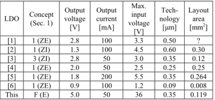
A comparison of the presented LDO to other selected LDOs is shown in Tab. 4.
The fact the error amplifier is anactive circuit enabled the use of the T-circuit R1L0-R1L1-R1L2 in Fig. 9 to avoid
LDO Concept (Sec. 1)
Output voltage [V]
Output current [mA]
Max. input voltage
[V]
Tech-nology
[μm]
Layout area [mm2]
[1] 1 (ZE) 2.8 100 3.3 0.50 ?
[2] 1 (ZI) 1.3 100 4.5 0.60 0.30
[3] 3 (ZI) 2.8 50 3.0 0.35 0.12
[4] 1 (ZE) 2.0 50 2.5 0.25 0.25
[5] 1 (ZE) 1.8 200 5.5 0.35 0.264
[6] 1 (ZE) 0.9 100 1.2 0.09 0.008
This F (E) 5.0 50 36 0.35 0.119
Tab. 4. Comparison of the presented LDO with the selected other LDOs: “F” – fractional-order control, “I” – internal output capacitor, “E” – external output capacitor, “Z” – compensation zero.
Acknowledgements
The authors wish to thank to Luděk Pantůček (ON Design Czech, an ON Semiconductor company) for directing the design of the presented LDO, and to Beth Johnston (ON Semiconductor) for grammatical and stylis-tic correction of this paper.
References
[1] CHAVA, C.K., SILVA-MARTINEZ, J. A frequency compensa-tion scheme for LDO voltage regulators. IEEE Transactions on Circuits and Systems I: Regular Papers, 2004, vol. 51, no. 6, p. 1041–1050. DOI: 10.1109/TCSI.2004.829239
[2] KA NANG LEUNG, MOK, P.K.T., SAI IT LAU. A low-voltage CMOS low-dropout regulator with enhanced loop response. In
Proceedings of the 2004 International Symposium on Circuits and Systems (ISCAS '04). Vancouver (Canada), 2004, vol. 1, p. 385–388. DOI: 10.1109/ISCAS.2004.1328212
[3] MILLIKEN, R.J., SILVA-MARTINEZ, J., SANCHEZ-SINENCIO, E. Full on-chip CMOS low-dropout voltage regulator.
IEEE Transactions on Circuits and Systems I: Regular Papers,
2007, vol. 54, no. 9, p. 1879–1890. DOI:
10.1109/TCSI.2007.902615
[4] WONSEOK OH, BAKKALOGLU, B. A CMOS low-dropout regulator with current-mode feedback buffer amplifier. IEEE Transactions on Circuits and Systems II: Express Briefs, 2007, vol. 54, no. 10, p. 922–926. DOI: 10.1109/TCSII.2007.901621
[5] AL-SHYOUKH, M., HOI LEE, PEREZ, R. A transient-enhanced low-quiescent current low-dropout regulator with buffer
impedance attenuation. IEEE Journal of Solid-State Circuits, 2007, vol. 42, no. 8, p. 1732–1742. DOI: 10.1109/JSSC.2007.900281
[6] HAZUCHA, P., KARNIK, T., BLOECHEL, B.A., PARSONS, C., FINAN, D., BORKAR, S. Area-efficient linear regulator with ultra-fast load regulation. IEEE Journal of Solid-State Circuits, 2005, vol. 40, no. 4, p. 933–940. DOI: 10.1109/JSSC.2004.842831
[7] MONJE,C.A., CHEN,Y.Q., VINAGRE,B.M., XUE,D., FELIU BATLLE,V. Fractional-order Systems and Control – Fundamen-tals and Applications. 2010, 430 p. ISBN 978-1-84996-334-3. DOI: 10.1007/978-1-84996-335-0
[8] CHEN, Y.Q. PETRAS, I., XUE, D. Fractional order control – A tutorial. In American Control Conference (ACC '09). St. Louis (USA), 2009, p. 1397–1411. DOI: 10.1109/ACC.2009.5160719
[9] VALSA, J., DVORAK, P., FRIEDL, M. Network model of the CPE. Radioengineering, 2011, vol. 20, no. 3, p. 619–626. DOI: 10.13164/re
[10] PETRZELA, J. Posouvače fáze založené na využití pasivních realizací fraktálních kapacitorů (Phase Shifters Using Passive Realizations of Fractal Capacitors). Slaboproudý obzor, 2014, no. 2, p. 6–12. ISSN 2336-5773 (In Czech).
[11] PETRAS, I. Fractional-order feedback control of a DC motor.
Journal of Electrical Engineering, 2009, vol. 60, no. 3, p. 117–128. ISSN 1335-3632
About the Authors ...
Libor KADLČÍK was born in Uherské Hradiště. He re-ceived his B.Sc. and M.Sc. degree in Electronics and Communication from the Department of Radio Electronics, Brno University of Technology, Czech Republic in 2011 and 2013, respectively. He is currently a graduate student in the Electronics and communication techniques (D-EST) program of the same department. He is a member of an analog ASIC design group at ON Design Czech, an ON Semiconductor company. His interests are analog electrical circuits, signal processing and programming.