A Comparative Analysis of Improved 8T SRAM Cell With
Different SRAM Cell
Aastha Singh
1, Preet Jain
1, Tarun Kumar Gupta
2 1Department of Electronics, SVITS, Indore, India 2
Department of Electronics, MANIT, Bhopal, India
Abstract
High speed and low power consumption have been the primary issue to design Static Random Access Memory (SRAM), but we are facing new challenges with the scaling of technology. The stability and speed of SRAM are important issues to improve efficiency and performance of the system. Stability of the SRAM depends on the static noise margin (SNM) so the noise margin is also important parameter for the design of memory because the higher noise margin confirms the high speed of the SRAM cell. In this paper, The proposed improved 8T SRAM cell shows maximum reduction in power consumption of 24.17% with 6T, of 88.6% with 7T, of 28.21% with 8T and of 35.03% with 9T, maximum reduction in delay of 9.1% with 6T, of 64.26% with 7T, of 9.18% with 8T and of 10.44% with 9T and maximum SNM of 35.02% with 6T, of 32.27% with 7T, of 34.4% with 8T and of 33.15% with 9T increases.
Keywords- Cadence tool, CMOS logic, Static Noise Margin, Delay and Power Consumption.
I.
INTRODUCTION
Static Random Access Memory is a type of RAM used in various electronic applications including toys, computers, digital devices and automobiles. The static RAM or SRAM only holds its contents while power is applied. An SRAM cell keeps the cell data for as long as the power is turned on since it consists of a latch and refresh operation is not required for the SRAM cell. Its difference from dynamic RAM is that DRAM must use refresh cycles to keep its contents alive. As indicated by the name, SRAM holds data/memory as a static image until written over or lost from powering down. SRAM is mainly used for the cache memory in microprocessors, mainframe computers, engineering workstations and memory in hand held devices due to high speed and low power consumption. Each bit in an SRAM is stored on four transistors that form two cross coupled inverters. Static Random Access Memories (SRAMs) are commonly embedded into system-on-chip (SoC) designs to store programs and data. Many efforts have been made to improve the efficiency of the SRAM. Improvements are reducing delay, power consumption and increasing stability. A significant increase has been there in the demand for low power and high performance digital VLSI circuits. Designers are implementing very high-order scaling of both device dimensions and supply voltage. Transistor density and functionality on a chip is improved by scaling. Scaling also helps to increase speed and frequency of the operation and hence higher performance. This paper is presented an improved 6T SRAM cell that has low power
consumption & high static noise margin than the other different SRAM cell.
II.
THE LITERATURE REVIEW OF
DIFFERENT SRAM CELLS
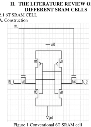
2.1 6T SRAM CELLA. Construction
Figure 1 Conventional 6T SRAM cell
state. SRAM cell is designed to provide write capability, non-destructive read access and data storage (or data retention) for as long as cell is powered. The design and analysis of different SRAM cells are: Conventional 6T, 7T, 8T, 9T and improved 6T. They are compared with respect to power, delay and speed. Generally, the cell design must strike a balance between cell area, speed, robustness, leakage and yield. One of the most important design objectives is power reduction. However, power cannot be reduced indefinitely without compromising the other parameters. As an example, low-power can compromise the cell area and also the speed of operations. The mainstream six-transistor (6T) CMOS SRAM cell is shown in Figure -1, here four transistors (M1−M4) comprise cross-coupled CMOS inverters and two NMOS transistors M5 and M6 provide read and write access to the cell. The most popular SRAM cell is a 6T CMOS SRAM cell due to its superior robustness, low-voltage and low power operation [9].
B. Operation of SRAM
The Static Random Access memory device can perform the operation which is as follows: hold, read and write.
a. Hold: The access transistors M5 and M6 disconnect the cell from the bit lines, if the word line is not asserted. The two cross coupled inverters formed by M1 – M4 will continue to reinforce each other as long as they are connected to the supply.
b. Read:
Figure 2 Read Operation of SRAM Cell.
The bit lines are pre-charged to VDD prior to initiating a read operation. The read operation is initiated by enabling the word line (WL) and connecting the pre-charged bit lines (BL_1 and BL_2) to the internal nodes of the cell. On read access, the bit line voltage VBL_1 remains at the pre-charge level as shown in Figure-2. The
complementary bit line voltage VBL_2 is discharged through transistors M1 and M5 connected in series. Conclusively, transistors M1 and M5 form a voltage divider whose output is now no longer at zero volts and is connected to the input of inverter M2−M4 (as in Figure -1). The sizing of M1 and M5 should ensure that inverter M2−M4 do not switch causing a destructive read [9].
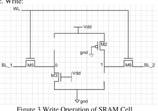
c. Write:
Figure 3 Write Operation of SRAM Cell.
2.2 7T SRAM CELL
Figure 4 A 7T SRAM cell
The circuit of 7T SRAM cell is made of two CMOS inverters that are connected cross coupled to each other with additional NMOS Transistor which is connected to read line and has two pass NMOS transistors connected to bit lines and bit line bar respectively. Figure-4 shows circuit of 7T SRAM cell, where the access transistors M5 is connected to the word-line (WL) to perform the access write and M6 is connected to the Read-line (R) to perform the read operations thought the column bit-lines (BL_1 and BL_2). The bit-lines act as I/O nodes carrying the data from SRAM cells to a sense amplifier during read operation or from write in the memory cells during write operations [12].
2.3 8T SRAM CELL
Figure 5 A 8T SRAM cell
The 8T SRAM circuit [13] is presented in this section. The schematic of the 8T SRAM cell sized for an 180nm CMOS technology is shown in Figure 5. The left sub-circuit of the 8T memory cell is a conventional 6T SRAM cell with minimum sized devices (composed of M1, M2, M3, M4, M5, and M6). Two data access transistors (M5 and M6) and
two bit lines (BL_1 and BL_2) are used for writing to the SRAM cell. An alternative communication channel (composed of a separate read bit line RBL and the transistor stack formed byM7 and M8) is used for reading the data from the cell.
Two separate control signals RWL and WL are used for controlling the read and the write operations, respectively, with the 8T SRAM circuit as shown in Figure 5. During a read operation, the read signal RWL transitions to VDD while the write signal WL is maintained at VGND. The read bit line (RBL) is conditionally discharged based on the data stored in the SRAM cell. The storage nodes (Node1 and Node2) are completely isolated from the bit lines during a read operation. The data stability is thereby significantly enhanced as compared to the conventional 6T SRAM cells [13].
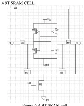
2.4 9T SRAM CELL
Figure 6 A 9T SRAM cell
Alternatively, for writing a “0” to Node2, BL_1 and BL_2 are charged and discharged, respectively. A “0” is forced onto Node2 through M6. During a read operation, RD signal transitions high while WL is maintained low and the read access transistor M9 is activated. Provided that Node1 stores “1”. BL is discharged through M7 and M8. Alternatively, provided that Node2 stores “1”, the complementary bit line (BL_2) is discharged through M8 and M9. Since M5 and M6 are cut-off, the storage nodes Node1 and Node2 are completely isolated from the bit lines during a read operation [14].
III.
IMPROVED 8T SRAM CELL
Figure 7 Improved 8T SRAM cell
The proposed SRAM cell is shown in Figure 7; it is made of conventional 6T SRAM with two additional PMOS and NMOS transistor. Over pull up & pull down network of two cascade inverter. In this new circuit NMOS transistor is connected to the pull down network of SRAM cell and other PMOS is connected to the Pull up network of the SRAM cell. The input of the gate of NMOS transistor of pull down network of the SRAM cell is connected Vdd and the input gate of PMOS transistor of pull up network of the SRAM cell is connected to ground which keep turn ON the transistor M7 & M8 throughout all operation of the SRAM. This whole modification in the circuit of the SRAM offers better improvement in comparison of 6T. A conventional 6T SRAM consumed more power due to its leakage problem but in the proposed circuit by the adding two transistor at pull up and pull down network leakage is reduced therefore the power consumption of the proposed circuit become less. The proposed improved 8T SRAM cell shows maximum reduction in power consumption of 24.17% with 6T, of 88.6% with 7T, of 28.21% with 8T and of 35.03% with 9T, maximum reduction in delay of 9.1% with 6T, of
64.26% with 7T, of 9.18% with 8T and of 10.44% with 9T and maximum SNM of 35.02% with 6T, of 32.27% with 7T, of 34.4% with 8T and of 33.15% with 9T increases. The read and write operation are similar to conventional 6T.
IV.
SIMULATION AND RESULTS
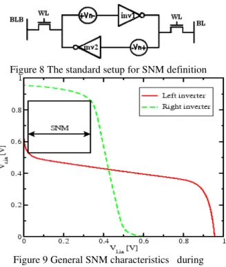
The Simulation and result of the improved 8T SRAM cell is presented in Table 1. In the following subsections, three important metrics of an SRAM design: Static noise margins, power, and delays are explaining.4.1 STATIC-NOISE-MARGIN (SNM)
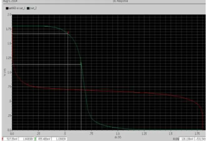
The stability of SRAM circuit depends on the Static Noise Margin. The basic SNM is obtained by drawing and mirroring the inverter characteristics and finding the maximum possible square between them. It is a graphical technique of estimating the SNM.
Figure 8 The standard setup for SNM definition
Figure 9 General SNM characteristics during Hold operation
second inverter to move to the right. The values of SNM vary in different operation modes. SNM is becoming important factor to check the stability during read operation. SRAM cell immunity to static noise is measured in terms of SNM that quantifies the maximum amount of voltage noise that can be tolerated at the cross-inverters output nodes without flipping the cell. The value of the SNM during cell operation changes with any change in the noise. Although the SNM is important during hold, the cell stability during active operation represents a more significant limitation to SRAM operation [8].
Figure 10 Butterfly curve for SNM of 6T SRAM cell
Figure11 Butterfly curve for SNM of 7T SRAM cell
Figure 12 Butterfly curve for SNM of 8T SRAM cell
Figure 13 Butterfly curve for SNM of 9T SRAM cell
Figure 14 Butterfly curve for SNM of Improved 8T SRAM cell
4.2- DELAY
time it takes for node A to go from 0.1V to 0.9V. In case of a write operation, write delay is defined as the time required for writing '0'to storage node 'L' from the time when word Line is activated to the time when 'L' falls to 10% of its initial high level. In the same way, writing '1' to 'L' is defined from the time when word Line is activated to the time when 'L' rises to 90% of its full swing from its initial low level. Write delay is approximately equal to the propagation delay of inv2 and inv l [2].
Figure 15 Simulated results for delay of 6T SRAM cell
Figure 16 Simulation results for delay of 7T SRAM cell
Figure 17 Simulation results for delay of 8T SRAM cell
Figure 18 Simulated results for delay of 9T SRAM cell
4.3- POWER CONSUMPTION
The power consumption of Static Random Access Memory cell depends on consumption of the power which used to perform the operation of the transistor [5]. Dynamic power consumption in SRAMs is consumed due to the charging and discharging capacitances during read and write operation and during each cycle of SRAM particular amount of Energy is drawn from the power supply and dissipated. For each cycle the power consumption is depended on the type of operation (read or write). Also, when the capacitor charged from GND to VDD and then discharged VDD to GND, the amount of energy drawn from the power supply and dissipated equals CLVDD2. The stored energy on the capacitor CL with voltage VC equals ½ CLVC2. Therefore, each time the capacitor CL is charged from VC to VDD and then discharged VDD to VC [3]. A average power dissipation of any device over one period can be obtained by following expression [6].
Pav = [(1/T) 0∫ T
I dt] × V
Figure 20 Simulated results for power consumption of 6T SRAM cell
Figure 21 Simulated results for power consumption of 7T SRAM cell
Figure 22 Simulated results for power consumption of 8T SRAM cell
Figure 23 Simulated results for power consumption of 9T SRAM cell
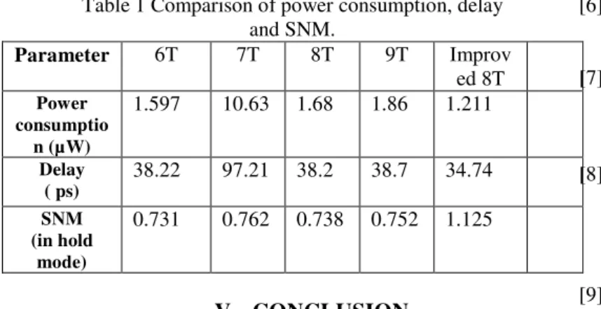
Table 1 Comparison of power consumption, delay and SNM.
Parameter 6T 7T 8T 9T Improv
ed 8T
Power consumptio
n (µW)
1.597 10.63 1.68 1.86 1.211
Delay ( ps)
38.22
97.21 38.2 38.7 34.74
SNM (in hold
mode)
0.731 0.762 0.738 0.752 1.125
V.
CONCLUSION
In this paper, we have design and implemented a low power, low delay and high SNM SRAM cell. We have also analyzed the power consumption and delay of improved 8T SRAM cell is less as compare to conventional 6T, 7T, 8T, 9T SRAM cell. The improved 8T SRAM cell is reducing the delay and increasing Static Noise Margin (in hold mode). In this paper, The proposed improved 8T SRAM cell shows maximum reduction in power consumption of 24.17% with 6T, of 88.6% with 7T, of 28.21% with 8T and of 35.03% with 9T, maximum reduction in delay of 9.1% with 6T, of 64.26% with 7T, of 9.18% with 8T and of 10.44% with 9T and maximum SNM of 35.02% with 6T, of 32.27% with 7T, of 34.4% with 8T and of 33.15% with 9T increases. Therefore, improved 6T SRAM cell is useful for high-speed and low power applications.
REFERENCE
[1] Ajoy C A, Arun Kumar, Anjo C A, Vignesh Raja: “Design and Analysis of Low Power Static RAM Using Cadence Tool in 180nm Technology”, IJCST Vol. 5, SPL - 1, Jan - March 2014.
[2] A. Islam and M. Hasan, Member: “Leakage Characterization of 10T SRAM Cell”, IEEE Transaction on Electron Device, Vol. 59, March 2012.
[3] Sushil Bhushan, Shishir Rastogi, Mayank Shastri: “High Density Four-Transistor SRAM cell with low power consumption”, IJCTA, Spt-Oct 2011.
[4] L. Chang: “An 8T-SRAM for Variability Tolerance and Low-Voltage Operation in High-Performance Caches”, IEEE Journal of Solid-State Circuits,Vol. 43, April 2008.
[5] Shyam AKASHE, Sushil BHUSHAN, Sanjay SHARMA: “High Density and Low Leakage Current Based 5T SRAM Cell Using 45 nm Technology”, Roman Journal of Information Science and Technology Volume 15, Number 2012.
[6] Kang S.-M., Leblebici Y., CMOS Digital Integrated Circuits-Analysis and Design, third edition, WCB McGraw-Hill, 2003. [7] Ramy E. Aly, Md I. Faisal and Magdy A.
Bayoumi: “Novel 7T SRAM cell for low power cache design”, 0 -7803-9264-71051$20.002005 IEEE.
[8] Nahid Rahman, B. P. Singh: “Design of Low Power Sram Memory Using 8t Sram Cell”, International Journal of Recent Technology and Engineering, Volume-2, Issue-1, March 2013.
[9] Sunil Kumar Ojha & P.R. Vaya: “A Novel Architecture of SRAM Cell for Low-Power Application”, ISSN (Print): 2278-8948, Volume-2, Issue-4, 2013.
[10] Michael C. Wang: “Low Power Dual Word Line 6-Transistor”, Proceedings of the World Congress on Engineering and Computer Science 2009 Vol 1 WCECS 2009, October 2009.
[11] K. Dhanumjaya, Dr. MN. Giri Prasad, Dr. K. Padmaraju , Dr. M. Raja Reddy: “Design of Low Power SRAM in 45 nm CMOS Technology”, International Journal of Engineering Research and Applications (IJERA), Vol. 1, Issue 4, pp.2040-2045. [12] Pankaj Agarwal, Nikhil Saxena: “Low
Power Design and Simulation of 7T SRAM Cell using various Circuit Techniques” International Journal of Engineering Trends and Technology (IJETT), Vol. 4, May 2013. [13] Sherif A.Tawfik and Volkan Kursun:
“Stability Enhancement Techniques for Nanoscale SRAM Circuits: A Comparison”,
International SoC Design Conference, 2008. [14] Zhiyu Liu and Volkan Kursun: