Abstract — The Cylindrical Surrounding Double-Gate (CSDG) Silicon on Insulator (SOI) Metal Oxide Field Effect Transistor (MOSFET) is a leading device for nanotechnology. This paper presents an effect of threshold voltage on symmetric CDSG MOSFET for the application of wireless sensors networks RF switches. By changing the structure from double-gate to CSDG MOSFET one can change the threshold voltage by which leakage current and short channel effects can be decreased. Hence the switching speed of RF switch can be controlled.
Index Terms — CSDG MOSFET, DG MOSFET, MIMO system, RF switch, Threshold voltage, Wireless sensor networks, VLSI.
I. INTRODUCTION
ireless sensor network (WSN) technologies have potential applications in communication, entertainment, travel, retail, industry, medicine, environment monitoring, scientific observation, field surveillance, structure monitoring and many other areas [1]. A wireless sensor network comprises small and distributed autonomous devices (e.g. nodes) which can sense physical phenomena. It processes the collected data and route them to the next node. Wireless sensors, sensor networks, pervasive computing, and artificial intelligence research together have the interdisciplinary concept of ambient intelligence in order to overcome the challenges [2]. Wireless sensor networks are an important technology for large scale monitoring, providing sensor measurements at high temporal and spatial resolution. The simplest application is sample and sends where measure are relayed to a base station, but WSNs can also perform in-network processing operations such as aggregation, event detection, or actuation [3]. The collaborative and low cost nature of wireless sensor networks brings significant advantages over traditional communication technologies as in electric power system. Example of some sensor network topologies are fully connected network, mesh network, star topology, and bus topology.
Manuscript received June 18, 2014, revised August 08, 2014. Viranjay M. Srivastava is with the Department of Electronic Engineering, Howard College, University of KwaZulu-Natal, Durban - 4041, South Africa.
(Corresponding author phone: 2759; fax: +27-31-260-2740; e-mail: [email protected], [email protected]).
WSNs have been widely useful in various aspects of electric power systems, including generation, delivery, and utilization [4]. The development of wireless sensor network has highlighted a wider range of applications due to flexible distribution of sensor nodes. In various applications, sensors must be completely embedded in detected objects and can hardly have physical connections to the outside world. The conventional solution is to use batteries, but due to disadvantages as bulky size, finite amount of energy, limited off-shelf life, and chemicals, that could cause a hazard. A wireless sensor network can operate by using a 3V battery only for few years. Systems with self-powered supply units potentially have a much longer life. Self-powered sensors provide the advantage free of the constraint of physical connections and battery maintenance [5].
In the sensor networks, switch has an important role. These switches are made up of PIN diodes, BJTs and MOSFETs. These switches have various threshold voltages. In this paper, various aspects of the threshold voltage have been proposed for a switch with CSDG MOSFET. Using the various threshold voltages, the reliability of the sensor devices with the application of CSDG MOSFETs can be stabilized
The scaling of MOSFET devices has been achieved by the advancement in the fabrication technology. To achieve the high integrated density device, the scaling down of devices is suitable process, It also improves the device performance. Due to reduction in the channel length the short channel effects and leakage current become important issue that degrades the device performance [6]. The double-gate (DG) MOSFET has two gates one on front side and another on back side. Both gates control the channel from both side and provide additional gate length scaling by factor of two. So the control on short channel effects can be better with DG MOSFET compared to the conventional MOSFET. The higher current density and low leakage can be easily obtained by using DG MOSFET [7, 8]. In a short-channel MOSFET, the depletion region has complicated 2D geometry and the channel region is influenced by the source/drain as much as by the gate. So to overcome these drawbacks a CSDG structure is proposed on next section.
The organization of the paper is as follows. The structure of CSDG MOSFET has been detailed in the Section 2. The sensor networks with transmission system have been analyzed in the Section 3. The modelings of device with reference to threshold voltage have been discussed in the
Effect of Threshold Voltage on
Cylindrical Surrounding Double-Gate MOSFET
for Wireless Sensor Networks RF Switches
Viranjay M. Srivastava, Member, IAENG
Section 4. Result and discussions with the challenges and its suggested solution have been discussed in the Section 5. Finally, Section 6 concludes the work.
II. INTRODUCTION OF CSDGMOSFET
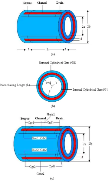
In the DG MOSFET, the gates are only on the two sides of the substrate. To utilize all the sides of substrate, we have widened the gate on the all-around the device and design like a cylinder. Therefore, we extend this structure to the Cylindrical Surrounding Double-Gate (CSDG) MOSFET [9]. It has less contact area with the board compared to the other MOSFETs. Due to the circular source and drain, the gate contact with the source and drain are on a long circular region, which avoids the gate misalignment. All the internal resistances and capacitances are shown in Fig. 1.
This CSDG MOSFET has threshold voltage, means a voltage after which channel forms and movement of the charges into the device starts. This creates the current into the device. With the change in length of the channel (distance between source to drain), the threshold voltage also varies. I will use this property for the WSNs in this paper.
(a)
(b)
(c)
Fig. 1. Schematic of the a) basic CSDG MOSFET, b) cross-section of CSDG MOSFET, c) Resistive and capacitive model of CSDG MOSFET
[9].
III. SENSOR NETWORK WITH TRANSMISSION SYSTEM
The wireless sensor structure is shown in Fig. 2. A sensor node is usually composed of power source and management, microprocessor, sensors, memory and wireless communication. This structure collects the data and processes as per the microprocessor and finally stored data and transmits accordingly. Power consumption in the sensor node is for sensing, communicating and data processing. Most of the power is needed for data communication in sensor node and is less for sensing and data processing.
Microprocessor performs tasks, processes data and controls the functionality of other components in the sensor node. Power consumption is less for the microprocessor because of is facility of sleep state. Radio frequency based communication is the most relevant that fits to most of the WSN applications. WSN’s use the communication frequencies from few kHz to 2.4 GHz. The functionality of both transmitter and receiver are combined into a single device known as transceivers are used in sensor nodes. Sensors and front end senses the data of the various frequency range. As in the Fig. 2 memory is there. The requirements of memory depend on the application means where the WSN will be used [1, 3, 7].
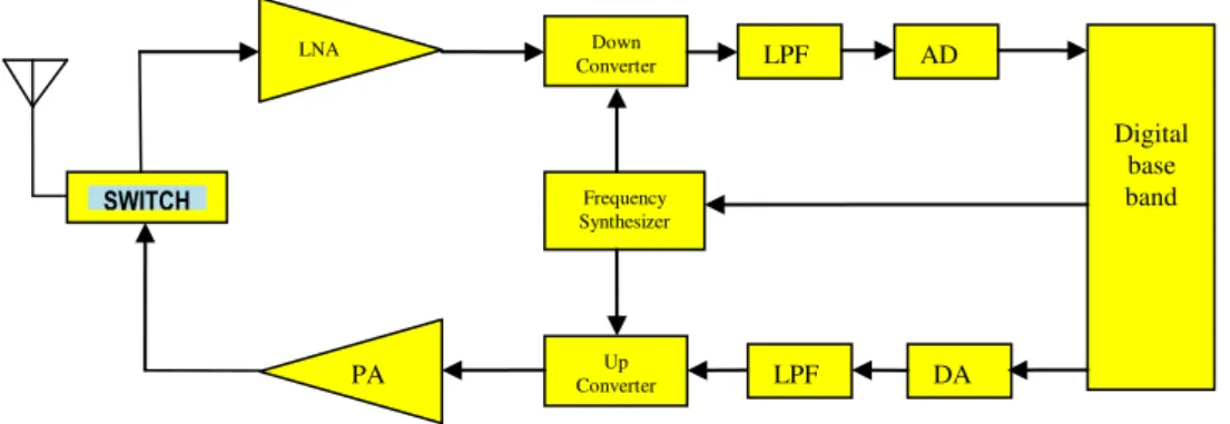
Wireless transmitters and receivers can be separated into two sections: one is baseband and other one is RF section. The baseband is the range of frequencies over which transmitters take their input and receivers produce their output. The RF section of the transmitter converts the processed baseband signal up to the assigned channel [10].
Fig. 3 shows the receiver’s front-end schematic. In receiver, the low noise amplifier (LNA) is the first gain stage in the receiver path. Thus, in an LNA, the signal must be amplified as much as possible, with a small signal to noise ratio decrease. This is achieved with the best noise figure. The LNA is an inductively degenerated common source amplifier. This makes the input impedance at 2.4 GHz equal to 50 Ω, for matching with an antenna switch [11].
For transmitter, the amplitude shift keying modulated signal is generated by means of a switched power amplifier. The power amplifier has a cascade of inverters in order to drive the ASK output signal to the input of the power amplifier.
For Frequency Synthesizer, the phase-locked loop has a reference generator circuit with a crystal-based oscillator at 20 MHz, followed by a phase-frequency difference circuit, a current steering charge pump, and a third-order passive filter. The passive section output is connected to the voltage-controlled oscillator that generates the desired frequency of 2.4 GHz.
Fig. 3. Simple RF transceiver architecture.
For antenna switch, the receiver or transmitter subsystems are connected to the antenna by means of a digitally controlled antenna switch. The isolation between non-connected ports must be high, keeping the losses between connected ports lowest. For a compact RF front end, the integration of the antenna switch must be in the same die of the transceiver [12]. In this structure for the switch I am using the CSDG MOSFET as discussed in the previous section.
IV. MODELING OF DEVICE WITH REFERENCE TO THRESHOLD
VOLTAGE
One can set the appropriate threshold voltage for the DG MOSFET device by providing channel doping but it degrades the device performance in terms of carrier mobility and dopant fluctuations. A large channel doping will also increase band-to-band tunneling leakage between the body and drain [13]. As a result, both channel doping and an asymmetric DG MOSFET result in degrading the device performance.
In the contrast of the above theory, the proposed CSDG MOSFET has facility of various threshold voltages for the device to design a RF switch. By using cylindrical engineering, the threshold voltage of CSDG MOSFET can be varied and one can able to maintain device performance and also able to get better result in terms of short channel effects and leakage current. The threshold voltage can be analyzed in from following three aspects:
A. Case I
Due the switch ON-resistance (RON), the value of threshold voltage varies according to the following equation:
. . T CTL
P ON L
V V
W K R
(1)
where ON 2
L R
a
for the simple MOSFET and
- 2
( - ) ON CSDG
L R
b a
for the CSDG MOSFET. It is clear
from these conditions thatRON RON CSDG , so the threshold voltage for the CSDG MOSFET will be lower as compared to the simple MOSFET. It shows that if four CSDG
MOSFETs are used for the RF switch, then all CSDG MOSFET can be set with different threshold voltage, which can be used for various sensors network as per requirements.
B. Case II
The ideal threshold voltage is determined by the following equations [14]:
0
2 (2 )
2 S A B
T B
qN V
C
(2)
where 2ψB is the surface potential to cause an inversion layer, NA is the semiconductor doping in the channel/substrate and Co is the capacitance of the oxide layer. The surface potential to cause an inversion layer, ψs(inv), is given by the equation:
2
( ) 2 ln A
S B
i
N kT inv
q n
(3)
After the formation of inversion layer, a drain voltage is applied to the MOSFET. As in the linear region, drain voltage is undersized at this time inversion layer has a constant resistance because of the linear V-I characteristics.
The above equation is valid for the simple MOSFET. For the CSDG MOSFET, to reduce the threshold voltage, following steps have been performed:
1) Semiconductor doping in the channel/substrate NA should be less, means nearly undoped so that due to its directly square root proportionality, it reduces the threshold voltage. But if in any application, higher threshold voltage is required one can change increase the semiconductor doping in the channel/substrate. 2) As the Semiconductor doping in the channel/substrate
(NA) decreases as the above condition, it reduces the inversion layer, ψs(inv). It also reduces the threshold voltage due to square root proportionality.
3) The capacitance of the oxide layer for the simple MOSFET is Co A
d
, now for the CSDG MOSFET
LPF AD
Digital base band
Down Converter
DA LPF
LNA
PA Converter Up
Frequency Synthesizer
2
ln
o CSDG
L
C
C
b a
, which shows that the Co ishigher for the CSDG MOSFET as compare to the simple MOSFET, so the threshold voltage decreases for the CSDG MOSFET.
C. Case III
In a MOSFET, the threshold voltage with the change in the source to bulk voltage, and the body effect is given as [15]:
0
(
2 - 2 )
T t SB
V
V
V
(4)where VT and Vt0 is the threshold voltage with substrate bias and the value of threshold voltage at VSB = 0, respectively. γ and φ are the body effect parameter and surface potential parameter respectively. A MOSFET with the non-zero source to body voltage has the threshold voltage modified with the body effect, that is if VSB ≠ 0, with VSB the source-body voltage which is for an n-MOSFET VB = VSS and for a p-MOSFET VB = VDD, then;
0 0
SB SB
thV thV
V
V
(5)For minimizing the threshold voltage, body effect parameter should be reduced to zero, which is a main feature of the proposed CSDG MOSFET [16]. It means in-between the application if I required changing the threshold voltage, it can happen with the change in the body effect parameter or by changing in the source to body voltage.
The importance of integrating large scale wireless telecommunication technologies such as 3G, Wi-Fi Mesh, and WiMAX has already been addressed by the researchers. Further improvements will be achieved by the coexistence of small-scale personal area technologies like radio frequency identification, bluetooth, ZigBee, and wireless sensor networks, together with large scale wireless networks to provide context aware applications [17].
V. RESULT AND DISCUSSIONS WITH THE CHALLENGES AND ITS SUGGESTED SOLUTION
From the analysis of the previous section, one can set the appropriate threshold voltage by changing the some parameters of CSDG MOSFET. The technical challenges [18] of WSNs applications and their suggested solutions are as follows:
1) In electric system environments, the topology and wireless connectivity of the network may vary due to link failures. Sensors may also be subject to RF interference, highly caustic or corrosive environments, high humidity levels, vibrations, dirt and dust, or other conditions that challenge performance [19]. These conditions and network topologies may cause a portion
of sensor nodes to glitch or obsolete data collection. With the use of CSDG MOSFET as component of switch the RF interference can be minimized. As if the four CSDG MOSFETs (in DP4T RF switch) will be used then the data will increase four time or same data at four places [8, 20]. In this circuit four CSDG MOSFETs are used, such that, if one pair gives false reading or data then another pair can verify this. 2) The variety of applications of WSNs for smart grid have
different quality of service requirements and specifications in terms of reliability, latency, network throughput, etc. Due to the use of four CSDG MOSFETs in a sensor networks, one can set each MOSFET with different quality of service. So, by using DP4T RF switch which has four CSDG MOSFETs means four types of quality of service at the same wireless sensor networks can be achieved. This may be in terms of reliability, latency, network throughput, etc. 3) In WSN, the bandwidth and communication latency at
each wireless link are location dependent and can vary continuously. This makes it very hard to meet quality of service requirements. The quality of services can be specified in terms of message delay, bit error rates, packet loss, transmission power, etc. Depending on quality of service, the installation environment, economic considerations, and the application, one of several basic network topologies may be used [21, 22]. But if the CSDG MOSFET based DP4T RF switch which will be used, then as per above explanation the quality of service can be easily meet.
4) The RF transceivers dissipate energy at a rate several orders of magnitude greater than processing units and memory. It is also of interest to note that transmitting and receiving incur similar energy drains [23]. According to the threshold voltage of the CSDG MOSFET as in Equation (1), (2), and (3), one can set the current and voltages of all the terminals of wireless sensors, so that the energy dissipation becomes small. It also increases the power and intensity of the transmit signal.
VI. CONCLUSIONS
REFERENCES
[1] Yunhao Liu, Yuan He, Mo Li, Jiliang Wang, Kebin Liu, and
Xiangyang Li, “Does wireless sensor network scale? A measurement
study on greenorbs,” IEEE Trans. on Parallel and Distributed
Systems, vol. 24, no. 10, pp. 1983-1993, Oct. 2013.
[2] Hande Alemdar and Cem Ersoy, “Wireless sensor networks for healthcare: A survey,” Computer Networks, vol. 54, no. 15, pp. 2688–2710, Oct. 2010.
[3] Peter Corke, Tim Wark, Raja Jurdak, Wen Hu, Philip Valencia, and
Darren Moore, “Environmental wireless sensor networks,”
Proceedings of the IEEE, vol. 98, no. 11, pp. 1903-1917, Nov. 2010.
[4] Vehbi C. Gungor, Bin Lu, and Gerhard P. Hancke, “Opportunities
and challenges of wireless sensor networks in smart grid,” IEEE
Trans. on Industrial Electronics, vol. 57, no. 10, pp. 3557-3564, Oct. 2010.
[5] Ping Li, Yumei Wen, Pangang Liu, Xinshen Li, and Chaobo Jia, “A magnetoelectric energy harvester and management circuit for wireless
sensor network,” Sensors and Actuators A: Physical, vol. 157, no. 1,
pp. 100–106, Jan. 2010.
[6] Viranjay M. Srivastava, K. S. Yadav, and G. Singh, “Analysis of double gate CMOS for double-pole four-throw RF switch design at
45-nm technology,” J. of Computational Electronics, vol. 10, no. 1-2,
pp. 229-240, June 2011.
[7] Thomas H. Lee, The Design of CMOS Radio-Frequency Integrated Circuits, 2nd Ed., Cambridge University Press, USA, 2004.
[8] Viranjay M. Srivastava, K. S. Yadav, and G. Singh, “Characterization process of MOSFET with virtual instrumentation for DP4T RF switch
–A review,” Wireless Sensor Network, vol. 3, no. 8, pp. 300-305, Aug 2011.
[9] Viranjay M. Srivastava, K. S. Yadav, and G. Singh, “Design and performance analysis of cylindrical surrounding double-gate MOSFET for RF switch,” Microelectronics Journal, vol. 42, no. 10, pp. 1124-1135, Oct. 2011.
[10] Behzad Razavi, “Challenges in portable RF transceiver design,”IEEE Circuits and Devices Magazine, vol. 12, no. 5, pp. 12-25, Sep. 1996. [11] Joao Paulo Carmo, Paulo Mateus Mendes, Carlos Couto, and Jose
Higino Correia, “A 2.4 GHz CMOS short-range wireless sensor network interface for automotive applications,” IEEE Trans. on Industrial Electronics, vol. 57, no. 5, pp. 1764-1771, May 2010.
[12] Gregory Chen, Scott Hanson, David Blaauw, and Dennis Sylvester,
“Circuit design advances for wireless sensing applications,”
Proceedings of the IEEE, vol. 98, no. 11, pp. 1808-1827, Nov. 2010. [13] Leland Chang, Yang kyu Choi, Ha Daewon, Pushkar Ranade,
Shiying Xiong, Jeferey Bokor, Chenming Hu, Tsu Jae King,
“Extremely scaled silicon nano-CMOS devices,”Proceedings of the
IEEE , vol. 91, no. 11, pp. 1860-1873, Nov 2003.
[14] “RF MOSFET - A product Manual,” Infineon Technologies,
www.infineon.com
[15] Frank Ellinger, Radio Frequency Integrated Circuits and Technologies, 2nd Ed., Springer Publication, 2008.
[16] Y. Cheng and M. Matloubian, “Frequency dependent resistive and
capacitive components in RF MOSFETs,” IEEE Electron Device
Letters, vol. 22, no. 7, pp. 333-335, July 2001.
[17] Bo Li, Yang Qin, Chor Ping Low, and Choon Lim Gwee, “A survey on mobile WiMAX [Wireless Broadband Access],”IEEE Communications Magazine, vol. 45, no. 12, pp. 70-75, Dec. 2007. [18] Vehbi C. Gungor and Frank C. Lambert, “A survey on
communication networks for electric system automation,” Computer Networks: The Int. J. of Computer and Telecommunications Networking, vol. 50, no. 7, pp. 877–897, May 2006.
[19] Vehbi C. Gungor and Gerhard P. Hancke, “Industrial wireless sensor
networks: challenges, design principles, and technical approaches,”
IEEE Trans. Ind. Electron., vol. 56, no. 10, pp. 4258–4265, Oct. 2009.
[20] Viranjay M. Srivastava, K. S. Yadav, and G. Singh, “DP4T RF CMOS switch: A better option to replace SPDT switch and DPDT
switch,” Recent Patents on Electrical and Electronic Engineering,
vol. 5, no. 3, pp. 244-248, Oct. 2012.
[21] Yide Liu, “Wireless sensor network applications in smart grid: recent trends and challenges,” Int. J. of Distributed Sensor Networks, vol. 2012, Article ID 492819, pp. 1-8, 2012.
[22]Frank L. Lewis, “Wireless Sensor Networks,” in Smart Environments: Technologies, Protocols, and Applications, John Wiley, New York, USA, 2004.
[23] Philippe Le Huy and Sebastien Roy, “Low-power wake-up radio for
wireless sensor networks,” Mobile Networks and Applications,