Diogo Miguel Esperança Garcia
Licenciatura em Ciência dos Materiais
Development of Large Area Paper Batteries
Dissertação para obtenção do Grau de Mestre em
Engenharia de Materiais
Orientadora: Professora Doutora Maria Isabel das Mercês Ferreira, Professora Associada, Departamento de Ciências dos Materiais da Universidade Nova de Lisboa
Co-orientadora: Doutora Cláudia Custódia Simão Delgado, Pos-Doc, Head of Printed Electronics Research Group, Department Functional Printing & Embedded Devices, Eurecat, Barcelona
Júri:
Presidente: Doutor João Paulo Borges, Professor Associado com Agregação do Departamento de Ciência dos Materiais, da Faculdade de Ciências e Tecnologia da Universidade Nova de Lisboa
Arguente: Doutora Ana Catarina Bernardino Baptista, Pos-Doc do Departamento de Ciência dos Materiais, da Faculdade de Ciências e Tecnologia da Universidade Nova de Lisboa
Vogais: Doutora Cláudia Custódia Simão Delgado, Pos-Doc, Head of Printed Electronics Research Group, Department Functional Printing & Embedded Devices, Eurecat, Barcelona
iii
Development of Large Area Paper BatteriesCopyright © Diogo Miguel Esperança Garcia, Faculdade de Ciências e Tecnologia, Universidade Nova de Lisboa.
v
“Intelligence is the ability to adapt to change.”
vii
Acknowledgments
Agradeço à Professora Isabel Ferreira pela oportunidade de desenvolver este trabalho numa área tão interessante e por nunca deixar de dar largas à imaginação, marcando a diferença em todos os ramos da sua investigação.
Um agradecimento à co-orientadora Claudia Delgado que me recebeu e integrou na unidade de Functional Printing na Eurecat, que ao longo de três meses me elucidou sobre o trabalho que tinha em mãos em todos os momentos, que tudo fez para me ajudar a cumprir os objetivos propostos, independentemente de estes serem mais ou menos realistas. Por me ter ajudado a conhecer a maravilhosa cidade de Barcelona, pela companhia nos jogos do mundial de futebol, pelos almoços e jantares, por ter contribuído para o alargar de horizontes nos mais diversos campos dentro da sua área e por ter tornado esta experiência ainda mais incrível, um enorme “obrigado”.
A todos os professores e investigadores do DCM, CENIMAT, CEMOP e restantes, por diariamente elevarem o nome desta casa cada vez mais alto e com isso facultar aos alunos cada vez melhores instalações, equipamentos, experiências e oportunidades aos alunos de Engenharia de Materiais e Engenharia de Microeletrónica e Nanotecnologias.
Um agradecimento especial Professor Fernando Santana, ex-diretor desta casa, pelo espírito FCTense que incutiu nesta escola, que espelha a sua boa disposição, descontração e compromisso com os alunos e futuro da instituição, por ser um exemplo.
Agradeço ao Professor João Paulo Borges por todo o trabalho feito como Coordenador do Mestrado Integrado em Engenharia de Materiais, por estar sempre presente e disposto a ouvir e defender os interesses dos alunos.
Ao António, pelo acompanhamento durante estes meses, pelo entusiasmo que sempre transmitiu a cada semana, pela ajuda a tentar entender e justificar todos os fenómenos estranhos que foram acontecendo, obrigado.
À Sofia, pela disponibilidade e paciência para me dar a conhecer e ensinar a utilizar o potenciostato e pela motivação e tranquilidade que sempre transmite.
A toda a equipa com que trabalhei na Eurecat, obrigado por me terem recebido tão bem, pela disponibilidade para me ensinarem a utilizar os mais diversos equipamentos e técnicas e pelas boas práticas de trabalho que me transmitiram. Um agradecimento especial ao Urbez, Joan, Bernat, Miguel, Dani, Moha, Paolo, Laia e Alejandra que foram acompanhando mais de perto este trabalho e que em alguns momentos contribuíram.
À Sónia Pereira, a minha orientadora do PIIC, por me ter deixado dar largas à imaginação e descobrir da melhor forma a vertente da investigação, obrigado.
Agradeço aos meus avós, que tanto contribuíram para ser o homem que sou hoje, por, desde sempre, me terem incentivado a perseguir os meus sonhos e ambições, por serem um exemplo de resiliência e dedicação.
Aos meus pais, por me terem trazido ao mundo, pela presença; preocupação; apoio e carinho constante, por sempre terem dado o melhor de si para me proporcionarem um caminho cheio de oportunidades e experiências incríveis e chegar até ao dia de hoje, por serem os meus símbolos de inspiração, um “obrigado” não chega.
Ao Paulinho, à Diana, ao Gonçalo e à Matilde, obrigado por me ensinarem a ser melhor irmão ano após ano, a partilhar, a ensinar, a brincar, a seguir os melhores exemplos e a querer ser cada vez mais um exemplo e inspiração para todos vocês. Um obrigado especial ao mais velho por tantas vezes ter aberto caminho para mim e por ao mesmo tempo ter sido um suporte e proteção nos melhores e piores momentos, pelas longas conversas e devaneios.
A toda a geração de 2013 de Materiais, pela união, companheirismo e pela força e espírito de grupo, desde o primeiro dia, até hoje.
À anTUNiA, por me ter ensinado a ensinar, por me ter ensinado a crescer em conjunto, por me ter dado histórias, memórias e amigos para a vida, por me ter mostrado que é possível viver a vida intensamente com organização e sucesso.
ix
Abstract
In this study was investigated a new strategy to fabricate paper-based batteries using screen-printing of metal powder-based pastes to prepare the electrodes. A piece of regular inkjet office paper is used, that serves not only as the substrate, but also as a porous separator between the electrodes. In this way, the developed device is a lithium-free paper battery.
The study includes different stages, such as electrodes redox pairs suitable with printing techniques, electrolyte composition and concentration and cell assembly. First, a silver/paper/carbon device was studied through cyclic voltammogram (CV) tests and from that was concluded the need of an electrolyte and encapsulation of the device in order to prevent water evaporation and losing its functionality. Different electrolytes combinations were investigated, samples geometry and design and cell assembly were tested and defined. The test and analysis of different electrode materials, such as silver, carbon, aluminum, nickel and zinc revealed the most suitable electrodes pair for achieving the highest capacitance performances. The zinc paste used did not perform well in terms of conductivity then it was decided to test its performance as an active layer between paper and electrode.
This approach was made with silver/paper/zinc-carbon structure device applying the electrode layers by bar coating technique. The results obtained in this device were promising then the final structure was performed with screen-printing technique. The device was fully characterized in terms of electrochemical performances using different electrolyte solutions, being the most suitable 5 M KOH aqueous solution.
The electrochemical characterization of the device consisted in electrochemical impedance spectroscopy (EIS), CV and scan rate influence. The samples were also characterized by SEM and XPS before and after the electrochemical studies. Charge-discharge and open circuit potential (OCP) studies were made to electrically characterize the device.
As a proof of concept, a red LED was powered by a single paper battery and also by a tandem structure of these paper batteries.
Keywords:
- Screen-Printing; - Paper Battery;
xi
Resumo
Neste estudo foi investigada uma nova estratégia para fabricar uma bateria à base de papel através da impressão de elétrodos por serigrafia a partir de pastas de pós metálicos. Um pedaço de papel vulgar de escritório é utilizado, não só como substrato, mas também como separador poroso entre os elétrodos. Desta forma, poderá ser alcançado um dos principais objetivos deste estudo, o desenvolvimento de uma bateria de papel livre de lítio.
O estudo é constituído por diferentes etapas, como a escolha de um par de elétrodos adequado às técnicas de impressão a ser utilizadas; composição do eletrólito e montagem do dispositivo. Em primeiro lugar, foi estudado um dispositivo do tipo prata/papel/carbono através de testes de voltametria cíclica (VC), dos quais se pôde concluir a necessidade de um eletrólito e consequente encapsulamento do dispositivo de forma a prevenir que a evaporação da componente aquosa do eletrólito e, por consequência, perdesse a sua funcionalidade. NaCl foi testado como eletrólito para a definição do desenho, geometria e método de inserção do eletrólito no dispositivo. Diferentes materiais como prata, carbono, alumínio, níquel e zinco foram testados e analisados para a escolha do par de elétrodos que proporcionasse melhor desempenho em termos de capacitância. A pasta de zinco utilizada não demonstrou desempenho positivo em termos de condutividade, no entanto, mais tarde, o seu desempenho como camada ativa, entre o papel e o elétrodo, foi testado.
A primeira abordagem foi numa estrutura prata/papel/zinco-carbono no qual os elétrodos foram depositados por bar coating. Os resultados obtidos foram considerados promissores, por este motivo a estrutura final foi aplicada por serigrafia. O dispositivo foi caracterizado em relação ao seu desempenho eletroquímico com recurso a diferentes eletrólitos, tendo sido obtidos os resultados mais satisfatórios para a solução 5 M KOH de base aquosa.
A caraterização eletroquímica do dispositivo consistiu nos estudos de espetroscopia de impedância eletroquímica (EIE), VC e influência do scan rate. As amostras foram também caraterizadas por microscopia eletrónica de varrimento (MEV), espetroscopia fotoeletrónica de raios-X (EFX) antes e após os estudos eletroquímicos. Foram também realizados estudos de carga-descarga e tensão de circuito aberto de forma a caraterizar eletricamente o dispositivo.
Para prova de conceito, um LED vermelho foi alimentado com recurso a uma única bateria de papel e também com uma estrutura tandem deste dispositivo.
Palavras-chave: - Serigrafia; - Bateria de Papel;
- Eletrónica Impressa e Flexível;
xiii
List of Tables
Table 1 – List of materials used for the device fabrication. ... 5 Table 2 – Calculated ionic conductivity, 𝛔𝒊, for regular office paper soaked in NaCl, KOH and NaOH electrolytes prepared in different molarities. ... 8 Table 3 – Reduction reactions and respective E0 for the selected metallic electrode materials. Adapted
from [48]. ... 9 Table 4 – Atomic percentage for the detected elements through SEM-EDS on zinc paste samples before and after photonic curing. ... 10 Table 5 – Anodic and cathodic peaks found with C/paper/Ni 1M NaCl sample 1 CV tests. ... 13 Table 6 – Anodic and cathodic peaks found with C/paper/Ni 1M NaCl sample 2 CV tests. ... 14 Table 7 – Potential achieved on the charging process of GCD studies in Ag/paper/C 1 M NaCl device. ... 16 Table 8 – Average Ag/paper/Zn-Ag OCP when soaked in different aqueous solutions. ... 17 Table 9 – Ag/paper/Zn-Ag detected elements analysis through SEM-EDS. Cells were analysed as printed and after the electrochemical studies with 5 M KOH. ... 20 Table 10 – Photonic curing parameters and resistance for each zinc paste sample. ... 31 Table 11 - XPS analysis of Zn samples’ surface before and after photonic curing. ... 32 Table 12 – SRS anodic peak values for C/paper/Ni cell soaked in 1 M NaCl between 20 and 120 mV/s. ... 32 Table 13 - SRS for Ag/paper/C cell soaked in Millipore water, between 20 and 120 mV/s, 3rd cycle
analysis for each scan rate. ... 32 Table 14- SRS for Ag/paper/C cell soaked in 1M NaCl, between 20 and 120 mV/s. 3rd cycle peak values
xv
List of Figures
Figure 1 - Schematic of a typical EES device. b) Ragone plot for comparison of EES devices. The diagonal lines reflect running time of the devices. Adapted from [20]. ... 2 Figure 2 - Schematics of a) electrochemical capacitors and b) batteries working mechanism. Adapted from [22]. ... 2 Figure 3 - Rectangular CV profile of an EDL capacitor and a CV plot with distinct Faradaic peaks from a battery, a) and b), respectively. Galvanostatic discharge profiles are represented on c) and d), the first is linear and corresponds to an EDL capacitor, the first shows the typical plateaus of batteries. Adapted from [22]. ... 3 Figure 4 - Schematic representation of a printed battery in the a) stack and b) coplanar architecture. . 3 Figure 5 - Schematic representation of a paper battery where a paper matrix behaves as substrate and porous membrane between the electrodes. ... 4 Figure 6 - Proposed geometry for the paper battery. ... 5 Figure 7 - Device fabrication representation. The printing and encapsulation processes are represented on steps 1-3 and 4-7, respectively. 1- A4 paper sheet heat treatment at 130 ºC (15 minutes). 2- Anode printing and subsequent film thermal curing at 130 ºC (15 minutes). 3- The cathode is printed on the opposite side of the sheet and then thermally cured at 130 ºC (15 minutes). 4- Cells are individualized and cut in the proposed device geometry. 5- Two conductive tape pieces are stick to the electrodes. 6- The device is immersed in the electrolyte. 7- Encapsulated device. ... 6 Figure 8 - Cell connection to AUTOLAB PGSTAT204 schematic representation. Adapted from [47]. .. 6 Figure 9 - a) OCP and b) CV plots of a dry silver/paper/carbon cell. c) and d) are the OCP and CV plots, respectively, of a new Ag/paper/C cell previously soaked in 0,15M NaCl electrolyte. OCP was measured at room temperature for 300 s. CV was performed at room temperature between -1 and +1 V, step size 0,5 mV and scan-rate 80 mV/s, in both cases the 3rd of 5 cycles is represented. ... 7 Figure 10 - a) Photograph of the two Au electrodes setup used in the EIS experiments within the paper ionic conductivity studies. b) Ionic conductivity vs electrolyte molarity plot. EIS measurements were performed at room temperature with the following parameters: 1 V DC voltage; 0,5 Vrms AC voltage; 1
MHz – 0,1 Hz frequency range and 5 points/decade. ... 8 Figure 11 - SEM cross-sectional images of zinc paste samples before and after photonic curing, obtained with Quanta 650 FEG on backscattered mode, 20 kV acceleration voltage and 500x magnification. a) Sample after bar coating procedure (no photonic curing). b) and c) were obtained after photonic curing from sample A6 but different regions were observed, a bright grey and less conductive area and a dark grey more conductive area, respectively. ... 9 Figure 12 - XPS spectra of Zn paste samples’ surface before and after photonic curing. ... 10 Figure 13 - a) OCP and b) CV plots for Ag/paper/Al cells soaked in 0,5M NaCl before and after the Al film evaporation. c) and d) are the OCP and CV plots, for Ag/paper/Al cells soaked in 1M KOH before and after Al deposition. OCP was measured at room temperature for 10 min. CV was performed at room temperature between -1 and +1 V, except for the 0,5M KOH Ag/paper/Al sample soaked after which was cycled between -1 and +3 V, step size 0,5 mV and scan-rate 80 mV/s, in both cases the 3rd of 5
cycles is represented. ... 11 Figure 14 - OCP measurement, a), and CV plots, b); c) and d), for Ag/paper/Ni cell soaked in 1M NaCl. OCP was measured at room temperature for 10 min. OCP was measured at room temperature for 10 min. CV measurements were performed at room temperature, step size 1,0 mV and scan-rate 80 mV/s. ... 12 Figure 15 - a) 10 min OCP plot for two C/paper/Ni soaked with 1M NaCl. b) CV plot (-0,5 and +0,7 V) for the first C/paper/Ni cell studied. c) SRS plot performed between 20-120 mV/s on the second C/paper/Ni sample. d) CV plot between -0,7 and +0,6V performed on the second sample at 80 mV/s, after the SRS. OCP was measured at room temperature for 10 min. SRS and CV were performed at room temperature, step size 0,5 mV. In both CVs the 5th, 50th and 100th cycles are represented. ... 13
Figure 16 - Ag/paper/C soaked in Millipore water studies. a) SRS plot performed from 20 to 120 mV/s. b) CV plot between -0,5 and +0,5 V for the 5th, 50th and 100th cycles, showing Faradaic peaks
Figure 17 - Ag/paper/C cells soaked in 1 M NaCl (a-b) and 1 M KOH (c-d) aqueous solution studies. a) SRS plot performed from 20 to 120 mV/s for 1 M NaCl cell. For each scan rate, the 3rd cycle is plotted.
b) 1 M NaCl cell CV plot between -0,5 and +0,5 V for the 5th, 50th and 100th cycles. c) SRS between 40
and 120 mV/s of 1 M KOH cell. d) CV plot for 1 M KOH cell performed in [-0,2; +0,6] V potential window, 5th; 50th and 100th cycles are plotted. SRS and CV were performed at room temperature, step size 5
mV. ... 15 Figure 18 - Ag/paper/C 1 M NaCl GCD plot. Black and blue represent the charge process with 0,1 and 0,2 mA, respectively. Red is the discharge stage, when there was no current (0 mA) applied. ... 16 Figure 19 - a) Electrode/paper/active-electrode proposed structure. b) Delamination between C and Zn pastes deposited by bar coating after C thermal curing. ... 17 Figure 20 - Ag/paper/Zn-Ag cells. a) 9x5,5 cm2 cell produced via bar coating. b) Screen-printed 2x2 cm2
cell compared with 2 € coin size. ... 17 Figure 21 - 10th cycle comparative CV plot for the tested solutions. CV measurements were performed at room temperature, step size 5 mV and 80 mV/s scan-rate. ... 18 Figure 22 - a) SRS; b) CV measurements’ plots from Ag/paper/Zn-Ag soaked in 5 M KOH. SRS and CV were performed at room temperature, step size 5 mV, 20-120 and 80 mV/s scan rate, respectively. ... 18 Figure 23 - XPS general spectra for Ag/paper/Zn-Ag cell as printed and after electrochemical studies with 1 M NaCl: a) Ag electrode; b) Zn-Ag electrode. ... 19 Figure 24 - Cross sectional images of Ag/paper/Zn-Ag cell as printed (left) and after electrochemical studies with 5 M KOH (right). ... 19 Figure 25 - Silver (top) and zinc-silver (bottom) electrodes’ images obtained through SEM, from Ag/paper/Zn-Ag cells as printed and after electrochemistry processes with 5 M KOH. ... 20 Figure 26 - Nyquist plot obtained for Ag/paper/Zn-Ag 5 M KOH device (left) and Li-ion battery (right). Adapted from [53]. EIS test of the fabricated Ag/paper/Zn-Ag 5 M KOH device was performed between 1 MHz and 0,1 Hz. ... 21 Figure 27 - First discharges of GCD tests on Ag/paper/Zn-Ag cells with 5 M KOH. Constant current discharges with: a) -50 µA and b) -0,1 mA applied. ... 21 Figure 28 - Cyclic GCD on Ag/paper/Zn-Ag 5 M KOH device. 1st and 2nd charging stages lasted 15 min,
while the rest took 20 min. +1 mA and -1 mA were applied for charging and discharging the device, respectively. ... 22 Figure 29 – Calculated area under charge and discharge curves for Ag/paper/Zn-Ag 5 M KOH 3rd GCD
cycle. ... 22 Figure 31 - Red LED powered by a single cell and tandem connection of Ag/paper/Zn-Ag 5 M KOH device. ... 23 Figure 30 - Single cell tandem connection prepared to proof of concept tests. ... 23 Figure 32 - SEM-EDS spectra and respective analysed region for zinc paste samples before (a) and b)) and after photonic curing on a brighter (c) and d)) and darker (e) and f)) areas. ... 31 Figure 33 - CV plot for the first 9x5,5 cm2 Ag/paper/Zn-Ag cell fabricated through bar coating and soaked
xvii
Acronyms
EES Energy storage system EDL Electric double layer CV Cyclic voltammetry
GCD Galvanostatic charge and discharge EIS Electrochemical impedance spectroscopy SEM Scanning electron microscopy
EDS Energy dispersive spectroscopy PET polyethylene terephthalate XPS X-ray photoelectron spectroscopy OCP Open circuit potential
xix
Contents
ACKNOWLEDGMENTS ... VII ABSTRACT ... IX RESUMO ... XI LIST OF TABLES ... XIII LIST OF FIGURES ... XV ACRONYMS ... XVII CONTENTS ... XIX
1. INTRODUCTION ... 1
1.1. PRINTED AND FLEXIBLE ELECTRONICS ... 1
1.2. ELECTRICAL ENERGY STORAGE DEVICES: SUPERCAPACITORS AND BATTERIES ... 1
1.2.1. Supercapacitors ... 1
1.2.2. Batteries ... 2
1.3. THE PATH TOWARD PRINTED PAPER BATTERIES ... 3
2. MATERIALS AND EXPERIMENTAL PROCEDURES ... 5
2.1. FABRICATION METHODS ... 5
2.1.1. Printing process ... 5
2.1.2. Electrolyte ... 5
2.1.3. Cell assembly and encapsulation ... 5
2.2. CHARACTERIZATION METHODS ... 6
2.2.1. Morphological characterization ... 6
2.2.2. Electrochemical studies ... 6
2.2.3. Electrical measurements ... 6
2.3. PROOF OF CONCEPT ... 6
3. RESULTS AND DISCUSSION ... 7
3.1. PRELIMINARY STUDIES ... 7
3.1.1. First approach to the silver/paper/carbon cell ... 7
3.1.2. Paper ionic conductivity study ... 8
3.1.3. Different electrodes for new devices ... 9
3.2. DEVICE STUDY ... 11
3.2.1. Ag/paper/Al ... 11
3.2.2. Ag/paper/Ni ... 12
3.2.3. C/paper/Ni ... 13
3.2.4. Ag/paper/C ... 14
3.2.5. Ag/paper/Zn-electrode final device ... 16
3.3. POWERING A LED ... 23
4. CONCLUSIONS AND FUTURE PERSPECTIVES ... 25
5. REFERENCES ... 27
6. APPENDIXES ... 31
6.1. ZN PASTE STUDIES ... 31
6.2. C/PAPER/NI CELL ... 32
6.3. AG/PAPER/C CELL ... 32
6.4. AG/PAPER/ZN-AG STUDIES ... 33
1
1.
Introduction
1.1. Printed and flexible electronics
Over the years, a number of printing technologies have been developed to take electronics from the common bulky rigid to flexible substrates. When the word “flexible” is used in electronics it means the device is: bendable, conformal shaped, lightweight, elastic, non-breakable, compatible with roll-to-roll fabrication, or large-area [1]–[3].
The development of flexible electronics has shown a lot of widespread applications such as wearable devices, flexible energy storage and conversion, sensors, displays, organic light-emitting diodes, antennas and transistors [4]–[6]. To date, most of the conductive electrodes needed to such devices on rigid substrates have been deposited by expensive and slow processes such as spin coating, sputtering, thermal evaporation and other clean room techniques. However, when using substrates such as paper, plastics or textiles, printing techniques like ink-jet printing, screen-printing, flexographic printing and gravure printing are more qualified to these rugged and flexible substrates. Printing technology enables the use of roll-to roll machinery which reduces the production costs and processing steps. This combination enables high speed fabrication of flexible devices [7]–[10].
1.2. Electrical energy storage devices: supercapacitors and
batteries
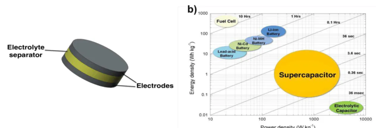
Batteries and electrochemical capacitors, also known as supercapacitors, are electrical energy storage (EES) devices and both rely on electrochemical processes in their operation mechanism. Although, they share a similar structure, typically composed by two electrodes and an electrolyte separator (figure 1 a)), the distinct processes occurring, in each one, determine their different charge storage properties. The electrolyte separator can be liquid, solid, or a porous membrane impregnated with a liquid electrolyte [11]–[14]. To better understand the working mechanism of EES devices such as supercapacitors and batteries it is important to understand the following three possible charge storage mechanisms: capacitive charge storage, non-capacitive Faradaic charge storage and capacitive Faradaic charge storage [15].
Capacitive charge storage is due to the electrostatic charge accumulation enabled by positive and negative charges residing at the interfaces between the electrodes and the electrolyte. This means no electron transfer takes place across the electrode interface, so, no chemical changes inside the solid phase of the electrode. At interfaces between solids and ionic liquids, this separation of electronic and/or ionic charges gives rise to an electric double layer (EDL). This mechanism is the core of EDL capacitors [15]–[17]. On a non-capacitive Faradaic charge storage process, the charge is stored by an electron transfer across the electrodes that produce chemical or oxidation state changes in the electroactive materials of the electrodes [18]. Capacitive Faradaic charge storage is the basis of pseudocapacitance and involves electron transfer reactions and hence the Faradaic processes in the electrode materials. This process is attributed to the so called pseudocapacitive materials, such as conjugated conducting polymers and transition metal oxides, which are capable of both Faradaic and capacitive storage of charge [11], [19].
1.2.1. Supercapacitors
Supercapacitors are a type of EES devices situated between batteries and conventional dielectric capacitors on a Ragone plot as shown in figure 1 b) [20]. They present lower energy than batteries, but higher cycle life and much higher power. These devices can be categorized on the basis of their energy storage mechanism into two: the double-layer supercapacitors and the redox supercapacitors. The first depends on the EDL formation and it is purely electrostatic. Pseudocapacitance is the basis of the redox supercapacitor charge storage mode (figure 2 a)). [16], [19], [21].
The electrodes for supercapacitors are usually made of activated carbon or its composites with polymers. Between the electrodes, the electrolyte separator is usually a porous gel membrane filled with a liquid electrolyte. The most widely used aqueous electrolytes contain solvated ions such as H+, K+,
OH- or SO
42- [11], [19].
1.2.2. Batteries
A battery, by definition, is one or more electrically connected electrochemical cells which contacts, or terminals, to supply electrical energy [14]. Battery’s structure also presents two electrodes and an electrolyte. One of the electrodes is positive while the other is negative, this nomenclature is based on their polarities, i.e., the positive electrode is always more positive, or has a higher potential than the negative one. According to the redox reactions occurring on each electrode, they can be called anode or cathode if it is oxidized (gives up electrons) or reduced (accepts electrons), respectively [11]. The electrolyte is the ionic conductor between the two electrodes. This is typically a aqueous liquid, which can have other solvents, with dissolved salts, acids or alkalis that impart ionic conductivity [23], [24].
In contrast with supercapacitors, the charge storage mode of batteries is only due to electrical energy conversion into chemical energy through Faradaic processes. During the discharging process, the electrochemical reactions occur at the anode and the cathode simultaneously and when connected to an external circuit, electrons are provided by the anode and collected at the cathode (figure 2 b)). It is possible to distinguish two types of batteries: primary batteries, which are used once and disposed, and secondary batteries, which can be recharged and used multiple times. The reactions occurring on primary batteries are irreversible, however, secondary batteries operate with reversible reactions [23]– [25].
Although different electrochemical systems are possible for batteries, Li-ion and Li-based batteries are the most commonly used once they present promising advantages of cheaper, lighter and smaller for the purpose of EES devices. Also lead-acid, Ni-Cd or Nickel Metal Hydride systems are possible, but they do not offer such high energy density as Li-ion complexes. The most used materials for the electrodes in Li-ion batteries are carbon, usually graphite, or lithium alloyed metals as the anode and a metal oxide such as CoO, LiTiO, NiO, MnCoO as the cathode. Battery electrolytes can be aqueous, non-aqueous or solid and the more widely used are aqueous KOH, LiPF6 and LiClO4 [14],
[26], [27].
3
Since rechargeable Li-ion batteries are used in billions of electronic devices such as laptops or electric vehicles, the demand for lithium and other materials related with Li-ion batteries is growing substantially. Cobalt and graphite share strong application on Li-ion batteries and both are considered critical raw materials. Although lithium is not yet considered a critical raw material there are some concerns about the supply risk of this material [28]–[31]. Moreover, beyond the mentioned concerns, the safety on Li-ion batteries is repeatedly questioned. Li-ion batteries can easily overheat, i.e., flammable substances inside the device can easily be ignited. Environmental issues are brought by the combustion of this substances since it releases a toxic gaseous mixture into the air [32].
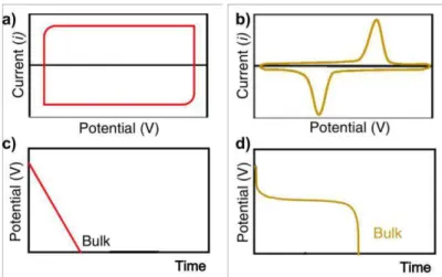
The CV plot of a battery is characterized by the presence of distinct peaks related to the Faradaic reactions occurring. GCD measurements usually present non-linear profiles with voltage plateaus which indicate the presence of two phases (figure 3 b) and d)) [13], [15], [22].
1.3. The path toward printed paper batteries
In the current world it is, due to the energetic and environmental crisis, more and more urgent to find news paths to prevent the exhaustion of non-renewable sources and to explore new cleaner and viable processes in an economical and environmental point of view. Aiming for the search of new or already existent materials that are recyclable, of low cost and present properties to allow the substitution of the widely used non-renewables ones is mandatory [33]–[35]. Paper is considered as a renewable material, not only because it is organic and biodegradable, but also because it can be obtained in a facilitated and sustainable way and can also be recycled at the end of its life. For this reason, the interest in the study of its properties and applicability on new devices for energy storage and conversion has been intensified [7].
Paper has already given proof of its applicability on electronic, EES devices and on fast and disposable diagnostic devices. Not only it presents low cost and easy obtainability, but also has interesting mechanical and electrical properties for the mentioned above applications [8], [33], [36]. This material has also high superficial area, caused by its microfiber composition, the ability to wick fluids via capillary action, strong adhesion to a variety of materials and is suitable for a wide range of printing technologies [37]. Two of the most frequently used printing techniques used to paper patterning are ink-jet and screen-printing and these require the use of specific inks with appropriate viscosity and surface tension [7], [38]–[41].
Figure 3 - Rectangular CV profile of an EDL capacitor and a CV plot with distinct Faradaic peaks from a battery,
a) and b), respectively. Galvanostatic discharge profiles are represented on c) and d), the first is linear and corresponds to an EDL capacitor, the first shows the typical plateaus of batteries. Adapted from [22].
Printed batteries are a consequence of combining printing and battery technologies. Conventional batteries design is usually rigid and bulky while for a printed battery the used substrate is frequently flexible. The main types for printed batteries are stack and coplanar architectures (figure 4), in the latter a separator is not required. Independently of the architecture, it is important to seal the printed battery in order to protect it from the exterior. Most of the state-of-the-art printed batteries are either Li-ion batteries or Zn/MnO2. Printed batteries offer many different attributes and features such as their thin
thickness, flexibility, fast and low cost fabrication, simple processing and reproducibility in multiple geometries [41], [42].
Paper, or paper-based composites, have already been used as the substrate on printed Li-ion; Zn/MnO2; Al/air; Zn/air batteries or bacteria-powered batteries for fast diagnostic devices [7], [8], [41],
[43], [44]. I. Ferreira et al. proposed a paper battery where a commercial paper sheet accumulates the functions of substrate and porous separator between the electrodes (figure 5). The cathode and anode were deposited by thermal evaporation, copper and aluminium, respectively, while air humidity (water vapour) was used as the electrolyte. This work resulted on a self-rechargeable device able to supply 0,6 V each which was then integrated in series in order to supply enough power to open and close the gate of a field effect transistor [45], [46].
The structure proposed by I.Ferreira et al. will be followed in this work. This differs from the already commercially available printed batteries since paper is still not used with this double function role of substrate and porous membrane between the electrodes [7][41].
5
2.
Materials and Experimental Procedures
The studied structure consists on a stack architecture where a commercial paper sheet is both the substrate and the separator of the device. The electrodes were printed on opposite sides of the substrate in a 2x2 cm2 (electrodes overlapping area) squared geometry (figure 6). A list of the used
materials is presented at table 1.
2.1. Fabrication Methods
2.1.1. Printing process
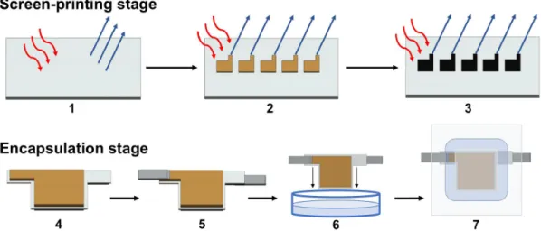
The electrodes were printed on regular office paper with a medium-sized pneumatic flat screen printer from ATMA (model AT-60FA). Non-commercially available nickel and zinc inks adhesion to paper was tested by bar coating (performed with K Control Coater from RK Printcoat Instruments, bar 3, velocity 3), previously to the screen-printing stage. Ni and Zn inks were also submitted to photonic curing, performed with NovaCentrix PulseForge 1200. Also, commercially available silver and carbon inks were screen-printed. 77T and 62T screens were used on the screen-printing process, depending on the ink. The printing process is represented at figure 7 from step 1 to 3. All heat treatments were performed on UN160 lab oven from Memmert.
2.1.2. Electrolyte
Aqueous NaCl, NaOH and KOH electrolytes were prepared in different molarities.
2.1.3. Cell assembly and encapsulation
Devices were encapsulate following the procedure on figure 7, from step 4 to 7. External contacts were prepared with two different conductive adhesive tapes of Cu and LAIRD. These were laser cut in a 0,5x9 cm2 rectangular geometry. Two different types of encapsulation were tested with Titer-Tops
sealing film and Fellowes 80 µm laminating pouch, both were previously cut in 6x6 cm2 squares. To
protect the device from any kind of glue and residues, two 3x3 cm2 polyethylene terephthalate (PET)
squares were placed between the paper device and the outer encapsulation film, one for each side. The lamination was performed, immediately after soaking the device in the electrolyte, on a Fellowes Venus A3 laminating machine using room temperature and the 80 µm temperature settings already installed in the equipment for Titer-Tops films and Fellowes laminating pouches, respectively.
Table 1 – List of materials used for the device fabrication.
Material Provider/Origin Used for/to/as
Ni paste Available at Eurecat Electrode printing Zn paste Available at Eurecat Electrode printing
Ag paste Dupont 5000 Electrode printing
C paste Dupont 7102 Electrode printing
Paper Unipapel 49998 Substrate
Water Millipore Water Electrolyte preparation
NaCl Panreac Electrolyte preparation
NaOH Sigma-Aldrich Electrolyte preparation
KOH Sigma-Aldrich Electrolyte preparation
Cu tape Godfellows Device external contact
LAIRD tape LairdTech Device external contact
PET Savic Device encapsulation
Titer-Tops Sigma-Aldrich Device encapsulation
Laminating pouch Fellowes ImageLast 80 µm Device encapsulation
2.2. Characterization Methods
2.2.1. Morphological characterization
Scanning Electron Microscopy (SEM) with Energy Dispersive Spectroscopy (EDS) with Quanta 650 FEG from ThermoFisher Scientific. X-ray Photoelectron Spectroscopy (XPS) were made with Phi-5500 XPS system.
2.2.2. Electrochemical studies
Open circuit potential (OCP), cyclic voltammetry (CV) and scan-rate influence studies were performed on AUTOLAB PGSTAT204 at Eurecat. EIS measurements were performed on Gamry Instruments Reference 3000 Potentiostat/Galvanostat/ZRA at FCT NOVA. All electrochemical studies were performed with two-electrode configuration following the suggestions of AUTOLAB user guide as shown on figure 8 [47].
2.2.3. Electrical measurements
Galvanic charge and discharge measurements were performed with AUTOLAB PGSTAT204. HM8118 Programmable LCR Bridge from HAMEG was used to measure the capacitance and resistance immediately after the device encapsulation.
Figure 7
-
Device fabrication representation. The printing and encapsulation processes are represented on steps1-3 and 4-7, respectively. 1- A4 paper sheet heat treatment at 130 ºC (15 minutes). 2- Anode printing and subsequent film thermal curing at 130 ºC (15 minutes). 3- The cathode is printed on the opposite side of the sheet and then thermally cured at 130 ºC (15 minutes). 4- Cells are individualized and cut in the proposed device geometry. 5- Two conductive tape pieces are stick to the electrodes. 6- The device is immersed in the electrolyte.
7- Encapsulated device.
7
3.
Results and Discussion
3.1. Preliminary studies
3.1.1. First approach to the silver/paper/carbon cell
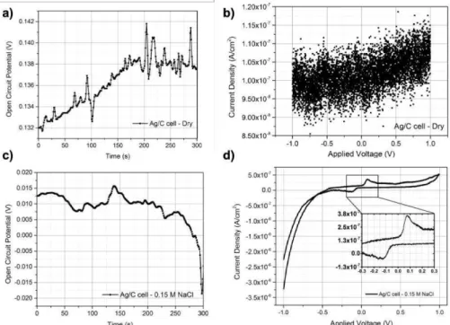
The electrodes for the firstly proposed device were silver (Ag) and carbon (C). Both the electrodes were previously screen-printed at Eurecat with equal thermal curing temperature and duration, 130 ºC and 15 minutes, respectively. One single layer of silver and two carbon layers were needed to achieve resistance values of 0.003 Ω and 300 Ω for each electrode, respectively.
OCP and CV measurements were performed with Gamry Instruments Reference 3000 Potentiostat/Galvanostat/ZRA at FCT NOVA. The aim for these measurements was to evaluate the need of a liquid electrolyte in the system and also the potential difference between the electrodes and the occurrence of internal short-circuits. The silver/paper/carbon (Ag/paper/C) cell was connected to the equipment totally dry, without any previous contact with any type of electrolyte.
Although OCP was only measured for 300 s, it is clear that there is a potential difference between the electrodes (figure 9 a)), meaning that no internal short-circuit occurred between the electrodes. Trough the CV plot on figure 9 b) it is not possible to observe the expected well-defined rectangular shape or any distinct peak. The measured current density values are in the order of 10-7 A/cm2. The
absence of a distinct shape on the CV plot can be explained by the high sensitivity of Gamry 3000 when measuring current values are lower than 10-6 A, which was the case, meaning that the measurement
might have been strongly affected by the surrounding electromagnetic “noise”.
To verify if higher current values were reached in the presence of a liquid electrolyte, a 0.15M NaCl aqueous solution was prepared. A new Ag/paper/C cell was soaked in the prepared solution and then the OCP and CV measurements were repeated with the same parameters. Again, a potential difference was verified between the two electrodes (figure 9 c)). The CV plot is presented in figure 9 d), this time it is possible to observe two distinct peaks and no internal short-circuits occurred. Considering that oxidative reactions are induced by anodic current when the scan direction is positive, while reductive reactions happen in the negative direction, it is possible to affirm that there is an anodic peak at 0.084 V and one cathodic peak at -0.152 V [24]. Though, the measured current density on the CV plot is about 10-7 A/cm2, the peak shaped CV is a result of an increase in the measured current, meaning that an
increase in charges mobility was caused by the presence of the liquid electrolyte.
These studies contributed to understand that a liquid electrolyte is needed to provide the necessary mobility of charges through the cell in order to trigger the electrochemical mechanism. Moreover, it is also possible to predict that the humidity achieved by the presence of a liquid electrolyte is also needed, so, the cell must be encapsulated in order not to dry.
3.1.2. Paper ionic conductivity study
Previous studies revealed that a liquid electrolyte was necessary. To understand the influence of the presence of a liquid electrolyte in paper’s ionic conductivity, three aqueous NaCl, NaOH and KOH solutions were prepared in different molarities. EIS measurements were performed to calculate the ionic conductivity following equation 1:
σ$ =&'×*), (1)
where σ$ is the ionic conductivity; R the measured resistance; L the paper thickness and A the cross-sectional area of the sample. Zreal measured values were considered as R to calculate σ$ (equation 2).
σ$=-& ./01×
)
*. (2)
The setup for this experiment is represented on figure 10 a). First, paper was immersed in the electrolyte for 600 s, then it was placed between two circular gold electrodes connected to the potentiostat through two pieces of carbon conductive tape and an EIS measurement was performed. Right after this first test, the sample was dried for 20 s with a hairdryer and then, a second EIS measurement occurred. Since gold electrodes’ diameter was 10.1 ± 0.01 mm, the considered A was 0.8 cm2.
Table 2 – Calculated ionic conductivity, 𝛔𝒊, for regular office paper soaked in NaCl, KOH and NaOH electrolytes prepared in different molarities.
Electrolyte Molarity (M) 𝐋(mm) 𝛔𝒊 (S/cm)
Wet Dry
NaCl 0.5 0.1 ± 0.01 (2.1 ± 0.2) × 10
:; (4.8 ± 0.4) × 10:>
1 0.1 ± 0.01 (9.2 ± 1.5) × 10:A (1.8 ± 0.2) × 10:B
KOH 0.5 0.1 ± 0.01 (1.6 ± 02) × 10
:; (7.4 ± 2.1) × 10:A
1 0.1 ± 0.01 (2.2 ± 0.1) × 10:; (5.0 ± 0.2) × 10:A
NaOH 0.5 0.1 ± 0.01 (1.1 ± 0.1) × 10
:; (0.8 ± 0.2) × 10:A
1 0.1 ± 0.01 (1.8 ± 0.6) × 10:; (4.7 ± 0.5) × 10:A
The obtained results are presented on table 2 and plotted on figure 10 b). No significant differences were observed between the samples soaked in 0.5 M and 1 M electrolytes when measuring their wet state. For this state, the highest ionic conductivity achieved was 2.2 × 10:; S/cm for 1 M KOH,
however all the other samples, with exception to the 1 M NaCl sample, demonstrated ionic conductivity values above 10-3 S/cm. Conventional Li-ion batteries require electrolyte’s ionic conductivity above 10-3
S/cm [24]. When in the dry condition, the highest σ$wasexhibited by 0.5 M KOH samples. It is important to notice that, unlike NaCl and NaOH, KOH samples did not show such a big loss in σ$ after the drying
9
It was not possible to measure paper’s ionic conductivity on its dry state, i.e., without its immersion on an electrolyte, because the equipment was not able to do it, again, it was close to the equipment’s minimum measurable current values.
3.1.3. Different electrodes for new devices
One of the purposes for this work was to try different cathode/anode combinations to build a paper battery. Thus, two positive and three negative standard reduction potential (E0) materials were chosen
according to their availability at DCM (FCT NOVA) and Eurecat. Silver and copper (Cu) were selected as positive electrodes while aluminium (Al), nickel (Ni) and zinc (Zn) were the negatives. Also, C electrodes were to be tested. The E0 values for the metallic electrodes, according to a specific reduction
reaction, are presented at table 3 [48]. The most positive and negative metals were Ag (E0≈+0.80 V)
and Al (E0≈-1.66 V), respectively.
Table 3 – Reduction reactions and respective E0 for the selected metallic electrode materials. Adapted from [48].
Reaction E0 (V) AgF+ e ⇌ Ag +0.80
CuF+ e ⇌ Cu +0.52
NiNF+ 2e ⇌ Ni −0.26
ZnNF+ 2e ⇌ Zn −0.76
Al;F+ 3e ⇌ Al −1.66
Nickel and zinc pastes available at Eurecat were tested on terms of adhesion to paper and, then, conductivity. Both succeeded to the adhesion tests performed by bar coating, however, only the first paste passed the conductivity tests with a measured resistance between 26 to 32 Ω, which is lower to the C electrodes printed before (300 Ω).
The zinc paste did not perform well on terms of conductivity, since it presented resistance values starting in 25 kΩ and increasing in time with a maximum measured value of 8 MΩ, this might be a consequence of Zn oxidation by air exposure. For this reason, photonic curing tests were performed as an attempt to achieve lower resistance values on 2x0.5 cm2 rectangular shaped samples. Different bank
voltages and pulse lengths were tried to achieve different strobe energy pulses, also, different number of pulses were influence was studied as shown at table 10 in Appendixes 6.1. Resistance measurements were made before and after every photonic curing step with a multimeter, having its test probes 1cm distant among themselves. Lowest resistance obtained was 15 kΩ (sample A4) for 280 V bank voltage; 3200 µs pulse length; single pulse, nevertheless, every sample presented its lowest resistance when a darker layer appeared on top of the initial bright grey Zn surface. Although these dust-like darker regions turned out to be more conductive, they were easily removed by the test probes, revealing, therefore, the original more resistive (5 MΩ) bright Zn layer below.
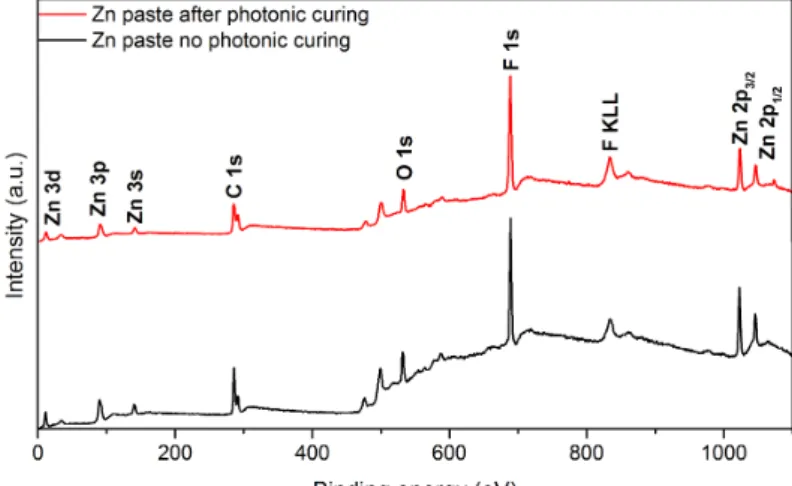
To morphologically characterize the Zn films, two samples were imaged with scanning electron microscopy (SEM). The first was not submitted to photonic curing and it is shown in figure 11 a), where it is clear to verify that a layer of flake-like structures, which corresponds to the Zn paste because its constitution is based on Zn flakes, is deposited on top of a darker layer, which is the office paper. In figure 11 b) and c) are shown two different regions of sample A6, which was cured in the photonic flash
oven, a brighter 6 MΩ area and a darker 160 kΩ area, respectively. Comparing the three studied conditions it is possible to notice that the top layer loses its flake-shaped structures after photonic curing, since its corners get rounded with this treatment. It is also possible to verify that A6 brighter and darker areas are distinct, since the latter’s top layer does not reveal any evidence of the initial flake-like structures as on the first. This area where Zn film turned into a darker grey colour indicates sintering of Zn particles, due to the absorbed energy from the photonic curing, partially oxidized.
SEM-EDS analysis were performed to elementally characterize the samples mentioned before. Table 4 presents the obtained results in atomic percentage for different elements detected by the equipment., according to the spectra showed on figure 31 in Appendixes 6.1. For every sample, the most detected element is carbon due to paper and Zn paste solvents’ organic composition. It is possible to notice that the percentage of Zn decreases with photonic curing, while fluorine (F) presence increases after this process. F has its origin in the paste’s binder, which is a fluorocarbon. Comparing the studied sample A6 areas, C and F percentage increase in the darker area, while Zn decreases. This last statement can be explained by the presence of the already mentioned dust-like layer that covered the Zn layer underneath, also, this might suggest that a dark dust-like fluorocarbon compound forms when the Zn paste is exposed to photonic curing. Also, calcium (Ca), magnesium (Mg), oxygen (O) and Al were detected, their presence is explained by the presence MgO, Al2O3 and CaO in paper’s constitution
[45].
Table 4 – Atomic percentage for the detected elements through SEM-EDS on zinc paste samples before and after photonic curing.
Element
Atomic % No
photonic curing
After photonic curing (sample A6) Bright area Dark area
C 45.73 44.77 46.99
O 8.86 7.00 10.46
F 11.11 15.94 20.73
Al 0.28 2.225 1.37
Ca 0.30 0.15 0.33
Zn 33.73 29.90 19.91
Mg - - 0.22
XPS measurements were performed on Zn paste samples, before and after the photonic curing process. The XPS spectra are showed in figure 12 and respective peak analysis, according to its binding energy (BE) is presented in table 11 (Appendixes 6.1). Although the samples were visually different, due to the, already mentioned, colour change, accordingly to the XPS spectra in figure 12, there is no significant difference between the two surfaces, since peaks disappearance or emergence was not observed.
11
silver/paper/aluminium (Ag/paper/Al) and carbon/paper/nickel (C/paper/Ni) cells were prepared by screen-printing and studied in section 3.2. It is possible to estimate the OCP value through the electrochemical cell potential (𝐸UVWWX ), calculated by equation 3:
𝐸UVWWX = Y𝐸UZ[\]^VX + 𝐸Z_]^VX Y. (3) However, the measured OCP is frequently different from the calculated 𝐸UVWWX , since equation 3
does not count with interfacial interactions and current leaks between the electrolyte and the electrodes [24].
3.2. Device study
The devices to be studied in this chapter were printed and encapsulated as described at 2.1.
3.2.1. Ag/paper/Al
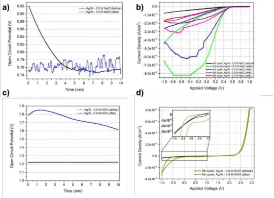
A first approach to Ag/paper/Al cell was made by evaporating a 1 µm thin film of Al onto screen printed Ag electrodes. A PET mask was drawn and then cut by laser in order to evaporate the Al films with the Ag electrodes’ geometry. Previously to the Al film deposition, two samples were soaked with 0.5 M NaCl by drop casting; other two samples were soaked with 0.5 M KOH by the same method and, finally, two samples without any electrolyte. The Al deposition was performed after the drop casted electrolytes evaporated, i.e., when the samples were dry. OCP and CV measurements were performed with Gamry 3000 Potentiostat. The calculated 𝐸UVWWX for the Ag/paper/Al cell is 0.86 V.
Ag/paper/Al sample with 0.5 M NaCl embedded previously to the Al deposition revealed an initial OCP of 0.92 V decreasing in time, unlike the sample soaked in the same electrolyte after Al deposition, 0.75 V initial OCP, however, the OCP measurement was not long enough to study this characteristic (figure 13 a)). CV plot for Ag/paper/Al soaked before the deposition did not reveal any shape, it was similar to straight line, meaning that there is current flowing, but no reaction occurred, showed in figure 13 b). Also, in figure 13 b), the CV plot for the samples on which the electrolyte was embedded after the Al deposition is presented, this time, some reactions occurred, however, the measured current density decreased more and more along the cycles. This diminish in the reaction’s current density can be a
consequence of irreversible product’s formation, giving rise to a passivation layer around the Al electrode.
The sample soaked in 0.5 M KOH before the deposition had 1.22 V as initial OCP, however the sample soaked after revealed higher OCP initial value around 1.78 V, figure 13 c). CV plots obtained for both 0.5 M KOH samples did not present any shape or reaction.
No Al paste was available to test the same structure with screen printed electrodes, nevertheless, similar results would be expected, since it tends to form a passive film and, then, becomes inactive [49].
3.2.2. Ag/paper/Ni
Encapsulated Ag/paper/Ni (soaked in 1 M NaCl) cell was firstly approached by OCP and CV measurements performed with AUTOLAB PGSTAT204, which are presented in figure 14.
Figure 14 a) reveals a tendency for the OCP value to stabilize close to -0.011 V after 10 min. Moreover, in the OCP plot is also possible to notice some disturbances at the first three minutes and later between the seventh and ninth minutes. The difference between the measured OCP and 𝐸UVWWX (0.54 V) can be justified by initial interfacial chemical reactions with the electrolyte that, in this case, are testified by the presence of the referred disturbances [24].
Three different CV tests, three cycles each, were made with three different voltage ranges, [-0.5; +0.5] V; [-1.0; +1.0] V and [-1.5; +1.5] V, the CV plots are showed in figure 14 b); c) and d), correspondently. None of the CV attempts was conclusive about the Ag/paper/Ni CV plot shape and if any oxidative or reductive reactions occurred systematically, i.e., it was not possible to notice a regular CV plot behaviour for this cell. Despite this, two oxidation peaks were found in figure 14 b) at +0.05 and +0.35 V while a single reduction peak was found between -0.16 and -0.18 V for second and third cycles. CV plot in figure 14 c) shows a single oxidation at 0.88 V, but only for the first cycle. In figure 14 d) is also possible to find a single oxidation peak between, +0.16 and + 1.16V on the second and third cycles, this time a reduction peak on the first cycle is found at -1.32 V.
13
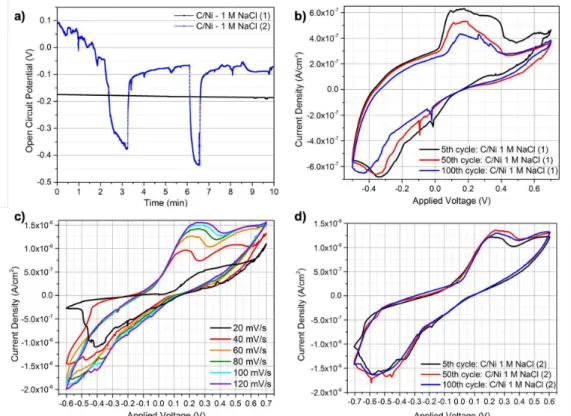
3.2.3. C/paper/Ni
Two C/paper/Ni cell samples were studied initially with 1 M NaCl. First, OCP was measured for 10 min for both samples. On CV tests, sample 1 was cycled between -0.5 and +0.7 V, while sample 2 was cycled between -0.7 and +0.6 V, for 100 cycles both. Previously to CV, sample 2 was submitted to a scan rate study (20-120 mV/s).
Both measured samples have OCP different than 0 V, this means that no internal short circuits occurred during the fabrication process. Considering the last measured value, samples 1 and 2 OCP showed -0.161 and -0.072 V, respectively. Unlike sample 1, sample 2 OCP suffered some disturbances in time that can be related to internal current leaks between the interfaces, as shown in figure 15 a).
CV plot for sample 1 is depicted in figure 15 b). In this CV plot it is possible to see one anodic peak and one cathodic peak, whose current density (Ipeak) and potential (Upeak) are displayed in table 5.
According to table 5, it is possible to notice that Ianodic peak decreased 1,99 × 10:a A/cm2 along the cycles,
while Icathodic peak, (modulus), decreased only 0.31 × 10:a A/cm2. This decrease can be a hint to a
quasi-reversible mechanism, since peaks got less intense with time.
Table 5 – Anodic and cathodic peaks found with C/paper/Ni 1M NaCl sample 1 CV tests.
Cycle Anodic peak Cathodic peak Ipeak(A/cm2) Vpeak(V) Ipeak(A/cm2) Vpeak(V)
5th 6.31 × 10:a +0.18 −6.82 × 10:a -0.34
50th 5.32 × 10:a +0.19 −6.61 × 10:a -0.35
100th 4.32 × 10:a +0.15 −6.51 × 10:a -0.43
A scan rate study (SRS) was performed on a new C/paper/Ni sample (sample 2) between 20 and 120 mV/s. Figure 15 c) depicts the SRS, the 3rd cycle of every scan rate is plotted. Observing the SRS
plot and table 12 (Appendixes 6.2) it is possible to notice that one anodic peak drifts apart with increasing scan rate. To better understand CV and SR, it is important to consider the reacting species diffusion to and from the electrode surface, where the reactions take place. The scan rate variation forces the diffusion layer thickness to vary. The diffusion layer can either be thick or thin for slow or fast scan rates. It is known that faster scan rates favour electrochemical irreversibility and, with that, peak’s potentials
drift apart [50]. Since, the present anodic peak’s potential on SRS plot slides apart from +0.18 V at 40 mV/s to +0.28 V at 120 mV/s, it is possible to confirm the quasi-reversibility of this reaction. Also, the same sample was submitted to 100 cycles CV measurements after the SRS. The obtained CV plot is shown in figure 15 d) and it is possible to observe that after 100 cycles, this C/paper/Ni 1 M NaCl preserves peak-shape without significant differences. Moreover, the presence of the previously observed anodic peak within the SRS is observed. Table 6 shows the peak’s current density and potential. Both cathodic and anodic peaks revealed an increase in their current density (modulus) between the 5th and 50th value, unlike between 5th and 100th when this value decreased.
Table 6 – Anodic and cathodic peaks found with C/paper/Ni 1M NaCl sample 2 CV tests.
Cycle Anodic peak Cathodic peak Ipeak(A/cm2) Vpeak(V) Ipeak(A/cm2) Vpeak(V)
5th 1.22 × 10:B +0.21 −1.62 × 10:B -0.58
50th 1.36 × 10:B +0.25 −1.80 × 10:B -0.59
100th 1.30 × 10:B +0.25 −1.64 × 10:B -0.57
Although, sample 1 and 2 were cycled between different voltage ranges, both revealed the presence of one anodic and one cathodic peak. Sample 1 oxidation peak was measured between +0.15V and +0.19 V while, the respective peak in sample 2 occurred between +0.21 and +0.25 V, meaning there is a small difference in terms of oxidation reaction potential among the two samples. Yet, the measured current density for this peak was different in one order of magnitude, 10-7 and 10-6 A/cm2
for sample 1 and 2, respectively. The same happened for the cathodic peak, but this time the reaction potentials were -0.43 to -0.34 V for sample 1 and -0.59 to -0.57 V for sample 2. Comparing samples’ CV plots, since its 5th, 50th and 100th plots are practically overlapped, it is possible to say that sample 2
behaviour more stable than sample 1. This C/paper/Ni structure was abandoned in this stage of the present thesis work, but further electrochemical, morphological, electrical and capacitive studies should be performed to attest this cell’s potential application on EES devices.
3.2.4. Ag/paper/C
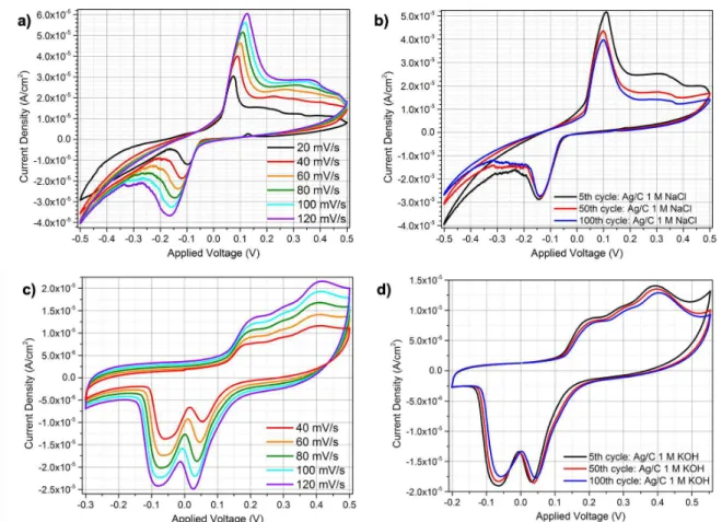
Since the results in section 3.1.1 seemed to be promising, new studies were performed to Ag/paper/C cells soaked in Millipore water, 1 M NaCl and 1 M KOH.
Millipore water was tested as an electrolyte for the Ag/paper/C cell with the purpose of understanding if its CV plot would be peak-shaped, i.e., if any Faradaic reaction would happen, and it would be different from other electrolytes. OCP was measured until it stabilized at -0.081 V for 20 s. Then, SRS was performed among 20 to 120 mV/s, the 3rd cycle for each scan rate is plotted in figure
16 a). Observing the figure 16 a) it is possible to verify the presence of two peaks, one anodic and one cathodic, and their current density increasing in modulus while the respective potential drifts as scan rate increases. This quasi-reversible behaviour is confirmed in table 13 at Appendixes 6.3 where Ipeak
and Vpeak are displayed. The anodic peak suffered a +4.18 × 10:B A/cm2 shift, while the cathodic peak
shifted −4.84 × 10:B A/cm2. The peak potential drift was less than -0.04 V for the reduction peak and
15
to evaluate the quasi-reversibility of Ag/paper/C soaked in Millipore water system, the CV plot in figure 16 b) shows a reduction in the peaks’ current density from the 5th cycle to the 100th. The loss in the peak
heights and relative amplitude, accompanied by the changes in the peak’s position (potential) might be a hint about the quasi-reversibility of the system.
To understand if Ag/paper/C CV behaviour would be different when the electrolyte was changed, a new cell was prepared, this time it was soaked in 1 M NaCl. The measured OCP for this system was -0.023 V. SRS and CV plots are showed in figure 17. Table 14 at Appendixes 6.3 is helpful for the SRS plot analysis. Again, one cathodic and one anodic peak are shown in both SRS and CV plots that suffer a −1.80 × 10:> and +3.01 × 10:>A/cm2, respectively, between the slowest (20 mV/s) and the fastest
(120 mV/s) studied scan rates, figure 17 a). The CV plot in figure 17 b) confirms that this system is not completely reversible when cycled between –0.5 and +0.5 V, since peak heights get reduced along the cycles. However, the cathodic reaction, accordingly to the CV plot, seems to be more stable/repeatable and the anodic one, since peak heights decrease is higher in the latter.
For the same purpose, 1 M KOH was tested as electrolyte in the Ag/paper/C cell and -0.237 V OCP was obtained. The SRS and CV plots in figure 17 c) and d), respectively show the presence of two cathodic peaks and a larger capacitive anodic region, which may include different anodic peaks. Peak heights, as seen before, increases with the scan rate on SRS. Until now, it is possible to affirm that different electrolytes give rise to different CV shape, number of peaks and their position and height, as seen for Millipore water, 1 M NaCl and 1 M KOH.
Since peak-shaped CVs are a property of batteries, GCD was approached with Ag/paper/C. The chosen electrolyte was 1 M NaCl. Charging constant current was applied for 30 s, while no current was applied for the discharge stage (5 min). Six GCD cycles were performed, 0,1 mA charging current was applied on the first three and 0.2 mA on the rest. Figure 18 shows the GCD plot for the six charge-discharge cycles. Since the CV shape for the 1 M NaCl sample was promising for a battery behaviour, the presence of linear plateaus on the GCD plots were expected. In table 7 the potential achieved for
Figure 17 - Ag/paper/C cells soaked in 1 M NaCl (a-b) and 1 M KOH (c-d) aqueous solution studies. a) SRS plot performed from 20 to 120 mV/s for 1 M NaCl cell. For each scan rate, the 3rd cycle is plotted. b) 1 M NaCl cell CV plot between -0.5 and +0.5 V for the 5th, 50th and 100th cycles. c) SRS between 40 and 120 mV/s of 1 M KOH cell.
each charging process is presented. Every discharge begins with a big potential drop, this can mean that part of the charge was not really stored, but the cell only suffered a polarization between the electrodes. However, after the first drop, a potential plateau above +0.1 V, which is higher than the -0.023 V OCP measured before, occurred for the last three cycles. Plateau’s presence is a synonym of a battery-like energy storage system. Since the last three cycles were performed with 0.2 mA and higher potential was achieve when charging, it might be possible to achieve even higher potentials if the charging lasts longer or if more current is applied.
Table 7 – Potential achieved on the charging process of GCD studies in Ag/paper/C 1 M NaCl device.
Current applied
(mA) Cycle
Final potential
(V)
0.1
1 1.20
2 1.23
3 1.23
0.2
4 1.36
5 1.37
6 1.39
Although the obtained GCD results were promising, such a big potential drop for a discharging process where no current is applied was not intended in this study, since, the device should be able to store electrical energy without this big potential drop. Having this in mind, the Ag/paper/C structure was abandoned.
3.2.5. Ag/paper/Zn-electrode final device
Since Ag/paper/C did not seem to be capable to store electrical energy and considering that, in batteries, the energy is charged by a conversion from electrical energy to chemical energy, the following question arises: does the Ag/paper/C structure have enough active material to chemically react and proportionate the needed conversion? As an answer, the idea of using an active layer between the paper and the electrode came up. Figure 19 a) shows the proposed electrode/paper/active-electrode structure. The purpose of this active layer was to add more reactive material to the system, so that energy conversion enhancement probability would be higher and with the stored energy would also increase. Since the conductive electrode would be printed on top, low electrical conductivity would not
17
technique. However, when while being thermally cured, the carbon electrode delaminated from the Zn layer under it. In figure 19 b) it is possible to find picture of the referred phenomenon. In an attempt to avoid it, more samples were prepared, but this time Zn layer was submitted to plasma surface treatment in order to improve the carbon paste adhesion. The same happened and the carbon paste was abandoned and replaced by silver, as a consequence of the incompatibility between Zn and C pastes when deposited though bar coating.
Ag/paper/Zn-Ag structure first attempt was made with 9x5.5 cm2 (electrodes overlapping area)
sample fabricated by bar coating. This time, there were no adhesion problems between Ag and Zn layers occurred. To study this structure’s viability, the fabricated cell was soaked in 1 M NaCl solution and then encapsulated. OCP and CV measurements were performed to prove that no short-circuit happened through the substrate, between silver electrode and Zn layer and also as a first approach to the electrochemical behaviour of this cell. For this cell, the OCP only stabilized after 212 s on +1.032 V. Also, the CV plot (figure 33 in Appendixes 6.4) for this cell was peak-shaped, meaning that Faradaic reactions existed and could be explored for the EES purpose.
New 2x2 cm2 Ag/paper/Zn-Ag cells were fabricated through screen-printing. Figure 20 exhibits
pictures of the fabricated cells via bar coating and screen-printing. In figure 20 b) it is possible to compare the screen-printed cells size with 2 € coin, both have similar sizes. In order to choose the final electrolyte to be used with this cell, 1 M and 5 M NaCl and 1 M; 5 M and 10 M KOH solutions were tested. The deliberation criterion was based on the CV plots obtained for the different solutions, the one that revealed highest peak heights would be chosen for GCD tests.
Due to NaCl limited solubility in water, it was not possible to achieve 10 M. Table 8 presents the average OCP measured for each tested solution. Highest OCP was obtained for 10 M KOH, moreover, it also possible to see that OCP (average) increased with solution’s molarity.
Table 8 – Average Ag/paper/Zn-Ag OCP when soaked in different aqueous solutions.
Solution Molarity
(M) OCP (V)
NaCl 1 5 0.9 ± 0.1 0.9 ± 0.1
KOH
1 0.9 ± 0.2
5 1.1 ± 0.2
10 1.1 ± 0.1
Figure 19 - a) Electrode/paper/active-electrode proposed structure. b) Delamination between C and Zn pastes deposited by bar coating after C thermal curing.
Figure 21 compares the 10th cycle CV plot for each solution tested. Analysing the referred figure
21, it is clear that cell soaked in 5 M KOH revealed the highest anodic and cathodic peaks. For this reason, 5 M KOH was chosen as the electrolyte for the GCD tests. Ag/paper/Zn-Ag 5 M KOH device SRS and CV are presented in figure 22. SRS in figure 22 a), as seen before in other structures, reveals quasi-reversible behaviour, since peaks position shifts in terms of potential. Faradaic mechanisms are confirmed by the presence of two anodic peaks and one cathodic peak. 10th cycle revealed the presence
of two anodic peaks at +1.96 V (60,7 mA/cm2) and +2.30 V (52.8 mA/cm2), also a cathodic peak at +1.21
V (-79.7 mA/cm2) was registered.
XPS measurements were performed in Ag/paper/Zn-Ag electrodes’ surface in two conditions: as printed and after electrochemical studies. In the latter situation, apart from the top surface analysis, the electrodes were also peeled with duct tape in order to analyse the interior layer of Zn, since the depth of analysis of a XPS measurement is 10 nm. Both Ag and Zn-Ag electrodes were characterized. The obtained general XPS spectra are displayed in figure 23. The analysis of XPS spectra peaks can be consulted in table 15 and 16 in Appendixes 6.4. Figure 23 a) shows the silver electrode general XPS spectra. As expected, before the electrochemistry studies, only C 1s; Ag 3d; O 1s and Ag 3p orbitals were detected. However, after the electrochemistry Na 2s; Zn 3p; Zn 3s, Cl 2p; Zn 2p and Na 1s appeared in both top surface and peeled conditions, again, this was expected due to the possible presence of Zn species moving through the liquid electrolyte, that in this case was NaCl and soaked the electrodes. The spectra in figure 23 b) only reveals the presence of Ag 3d; Ag 3p; O 1s and C 1s on the electrode’s surface before electrochemistry, since XPS is only a superficial technique, it was not expected to see any peaks related to Zn. After the electrochemical studies, Zn 3d; 3p; 3s and 2p peaks