September,2018
Tomás Sousa Lopes
Bachelor in Micro and Nanotechnologies Engineering
Metal layer for enhancing optical reflection in passivation
layers in thin film solar cells
Dissertation for obtaining the degree of Master of Science in Micro and Nanotechnology Engineering
Supervisor: Doctor Pedro Salomé, Group Leader, International Iberian Nanotechnology Laboratory
Co-Supervisor:
Doctor Manuel J. Mendes, Post Doc Fellow, Faculty of Sciences and Technology, New University Of Lisbon
Examination Commitee: Chairperson: Dr. Prof Rodrigo Martins Rapporteurs: Dr. Prof. Pedro Salomé
Metal layer for enhanceng optical reflection in passivation layers in thin-film solar cells
v
“Blood, sweat and tears”
vii
Acknowledgments
This master thesis marks the end of my 5 year journey. As such I, in this section would like to acknowledge who help trough this journey. As such a big thank you to all.
Primeiramente, quero agradecer ao Prof. Dr. Rodrigo Martins e à Prof. Dr. Elvira Fortunato pela oportunidade de poder estudar neste curso, bem como de utilizar as instalações do CENIMAT e CEMOP durante a minha estadia. Um especial obrigado ao professor Hugo Águas, por ter informado da oportunidade de realizar esta tese de mestrado no INL.
Ao meu orientador, Prof. Dr. Pedro Salomé, por me ter recebido de braços abertos no seu grupo de investigação, durante este período. Não há palavras para agradecer todo o apoio que me forneceu durante a minha estadia no INL. Estou extremamente agradecido, por todas as discussões de resultados, os seus ensinamentos, a disponibilidade e o esforço que fez para arranjar tempo para as minhas dúvidas. Por tudo isto um grande obrigado!
Um especial obrigado ao Dr. Paulo Fernandes, por toda a sua boa disponibilidade, a sua transmissão de conhecimento, bem como pela ajuda e discussões que me ajudou a melhorar o meu manuscrito.
Um obrigado ao meu orientado na FCT, o Prof. Dr. Manuel Mendes, que me acolheu durante uma semana e pela sua grande ajuda nas simulações e pelas suas respostas as minhas questões durante o período da tese. Grande obrigado.
Ao Miguel Cunha, um grande agradecimento por toda a ajuda que me forneceu durante estes meses. Por toda a sua disponibilidade para as minhas dúvidas, os dias passados na sala limpa, por todo o apoio que me deu durante estes seis meses, bem como o tempo que teve a rever o manuscrito, um grande obrigado!
To Sourav Bose, for all the help and guidance during our cleanroom work, the teachings he gave me as well as for his big counsel on to write my thesis with “my eyes closed”. I hope that someday you will start drinking coffee again.
Para as outras pessoas que estiveram comigo no grupo ao longo destes meses. Ao Barbosa, por toda a sua ajuda na sala limpa, comentários para o manuscrito e também para todos os cafés que me tirou para me focar na escrita. Ao Ricardo, pela sua ajuda no inicio quando cheguei a braga e pelos dias em que ficávamos os dois até tarde no INL. Á Beatriz, pela sua boa disposição que contagiou o grupo todo, pelas suas sugestões de organização e também pelos amendoins que providenciou. Ao André e para a Célia que pelos os seus comentários perspicazes que ajudaram a melhor o manuscrito.
To INL staff that helped during my work. A big thanks to Jerome for being 100% available to us and for the e-beam exposures, to José for his availability and his help during the deposition and to Mariam for all the help she gave me, a big thank you.
A special thanks to Sirazul, Manuel Chapa and Miguel Alexandre, for all the help they gave me for the optical simulations.
Á minha outra família: os Grossos. Ricardo, Pera, Breno, Catela, André, Miguel, Opinião, Paulo, William, Raul, Gonçalo, Campoa. Obrigado por tornarem estes 5 anos, os melhores da minha vida. Todas as festas, jantares e momentos passados juntos irão estar para sempre comigo. É verdade em os amigos da faculdade são para a vida e eu tenho a certeza que vos levo para vida toda! Tambem não podia deixar de agradecer à Catarina e à Maria, por sempre estarem lá e por todos os momentos que passamos nestes 5 anos.
Um agradecimento ao Filipe Peixoto, o meu padrinho. Por todos os momentos passados, os chás ás 2 da manhã, as viagens para a cidade Universitária para os jogos bem como todas as festas, um grande obrigado!
Aos meus pais e irmãos, que sem eles esta aventura não seria possível! Por todo o seu apoio e carinho que me deram, especialmente nestes meses que passei em Braga. Já está quase a acabar, Mãe e Pai!
ix
Abstract
Thin film, CIGS solar cells were able to achieve efficiency values higher than multicristalline silicon solar cells (22.9 % vs 22.3 %). However, a possible In scarcity, may increase its production costs, hence decreasing the CIGS thickness is of upmost importance for the technology to stay cost-competitive. However, when decreasing the CIGS thickness two main efficiency limitations arise; rear contact recombination and optical losses due to incomplete light absorption. The main focus of this thesis is to increase the rear optical reflection of an ultrathin CIGS solar cell. For that, six different metals (Ag, Au, Cu, Ta, Ti and Zn) and two metallic alloys (AlSiCu and TiW) were tested as possible candidates for increasing the rear optical reflection and a nanopattern point structure was employed with Al2O3 as the
passivation layer. Optical simulations were conducted to verify which metals gives the highest enhancement at increasing the light absorption in the CIGS layer. The solar cells fabricated were heavily affected by the reaction of the metal layer with the CIGS. As such, an alternative solar cell architecture was developed to prevent such reaction by depositing a Mo layer to cover the point contacts. In the end, the solar cell that incorporate a TiW layer, managed to achieve a 3.69 % (absolute) enhancement in efficiency values over the reference solar cell.
Keywords: CIGS, metallic layer,rear reflection, optical simulation, TiW,
xi
Resumo
Células solares de filme fino CIGS, conseguiram valores de conversão de energia superiores aos conseguidos por células solares de silício multicristalino (22.9 % vs 22.3%). Contudo, uma possível escassez de In pode levar a um aumento de custos de produção, consequentemente, uma redução de espessura da camada CIGS é altamente importante, para a tecnologia manter-se competitiva em termos de custo de produção. Contudo, ao reduzir a espessura do CIGS, dois problemas, que limitam a conversão de energia, surgem: a recombinação nas interfaces e a incompleta absorção de luz. O grande foco desta tese é de aumentar a reflecção optica traseira de uma célula solar ultrafina CIGS. Para tal, seis metais (Ag, Au, Cu, Ta, Ti e Zn) e duas ligas metálicas ( AlSiCu e TiW) foram testados como possível candidatos, uma estrutura nano-padronizada com pontos de contacto foi utilizada e Al2O3 foi
utilizado como camada de passivação. Simulações óticas, foram realizadas para averiguar qual metal dá o maior aumento na absorção de luz no CIGS. As células solares fabricadas, foram altamente afetadas pela reação da camada metálica com o CIGS e Se. Uma nova estrutura foi desenvolvida para prevenir tal reação ao depositar uma camada de Mo para cobrir os pontos de contacto. No final, a célula solar que incorpora TiW conseguiu um aumento (absoluto) de 3.69 % em conversão de energia sobre a célula solar de referência.
xiii
Contents
Acknowledgments ... vii
Abstract ...ix
Resumo ...xi
Contents ... xiii
List of figures ... xv
List of tables ... xvii
Symbols ... xix
Acronyms ... xxi
Motivation and objectives ... xxiii
1 Introduction ... 1
1.1 Solar cell parameters ... 1
1.2 CIGS solar cell ... 2
1.2.1 State of the art ... 3
1.2.2 CIGS material ... 3
1.3 Passivation effect ... 4
2 Materials and methods ... 7
2.1 Solar cell fabrication and deposition techniques ... 7
2.2 Characterization techniques ... 9
3 Results and discussion ... 11
3.1 Numerical model ... 11
3.1.1 Optical characteristics with ultrathin absorber... 12
3.1.2 Simulations for solutions of increasing the rear reflection at the rear contact ... 13
3.2 Sample fabrication ... 15
3.2.1 Substrate characterization ... 15
3.3 Solar cells characterization ... 17
3.3.1 Solar cells relative reflectance ... 17
3.3.2 Electrical characterization ... 18
3.4 Alternative CIGS solar cell structure for enhancing light absorption ... 21
3.4.1 Structure development ... 22
3.4.2 Samples characterization ... 24
4 Conclusions and future perspectives ... 29
5 References ... 31
6 Annexes ... 35
6.1 Annex A: CIGS bandgap determination ... 35
6.2 Annex B:Supplementary figures ... 36
xv
List of figures
Figure 1.1) A solar cell equivalent circuit;b) Current-voltage curve characteristics of a solar cell under
illumination. Adapted from[17] ... 1 Figure 1.2 - Conventional solar cell structure, not at scale ... 2 Figure 1-3 - The crystal structure of CIGS. The colours indicate copper (red), selenium (yellow) and indium
(blue). The indium atoms can be replaced be Ga.[31] ... 3 Figure 1.4 - Schematic representation of the rear of (a) a p-type Si solar cell with a surface passivation stack and
micron-sized local point contacts and (b) CIGS solar cell with a surface passivation stack and nano-sized local point contacts. Also the typical base/absorber thickness, minority carrier diffusion length, contact opening diameter and distance between contact openings are specified [34]. ... 4 Figure 2.1 - Standard step by step fabrication for a CIGS solar cell. In this thesis the fabrication will occur
between the Mo deposition and the absorber growth. Not on scale ... 7 Figure 2.2 - a) Representation of the structure obtained after the resist removal; b) Schematic showing the
fabrication steps. Both figures are not on scale ... 9 Figure 3-1 - a) simulated CIGS absorptance for an ultrathin solar cell and a regular solar cell with a 2µm
absorbed layer (solid lines), parasitic light absorptance at the rear contact ( dashed lines); b) simulated solar cell reflectance for ultrathin solar cell and a regular solar cell with a 2µm absorbed layer. The calculated JSC
for the ultrathin solar cell was of 30.30 mA/cm2 and 33.85 mA/cm2 for the standard solar cell ... 12 Figure 3.2 a) CIGS absorptance for all solar cells simulated; b) total solar cell reflectance for the solar cells
simulated; c) parasitic light absorptance at the rear contact for the simulated solar cells. ... 14 Figure 3.3 - CIGS absorptance for a regular solar cell with a 2µm CIGS solar cell and for the ultrathin solar cell
with Ag as a metallic layer (Mo/Ag/Al2O3) ... 14 Figure 3.4 -SEM top-view images of the samples Mo/Al2O3 (a) and Mo/TiW/Al2O3 (b). The images show the
pitch dimensions as well as the hole diameter. A expected 2μm pitch is achieved, the hole diameter is
elongated in a particular direction due to e-beam astigmatism. ... 16 Figure 3.5 - Measured reflectance of all the samples fabricated prior to the absorber growth. A kink is observed
at around 900 nm, due to a change in the detector in the system. Reflectance relative to a BaSO4 reference. ... 17 Figure 3-6– Measured relative reflectance of the solar cells fabricated. ... 18 Figure 3.7– Illuminated J-V curves of all the solar cells fabricated: a) Mo/Au/Al2O3, Mo/Cu/Al2O3, Mo/Al2O3
, Mo/Ti/Al2O3, Mo/AlSiCu/Al2O3 and for Mo/Ta/Al2O3; b) for Reference -II,, Mo/Ag/Al2O3,
Mo/TiW/Al2O3-I Mo/Zn/Al2O3 and Mo/TiW/Al2O3-II; c) EQE measurements ... 21 Figure 3.8 - a) representation of the structure obtained after the lift-off; b) Schematic showing the fabrication
steps. Both figures are not on scale ... 23 Figure 3.9-Post development optical microscope pictures of samples: Mo/Al2O3 (a) and Mo/Ag/Al2O3/Mo (b).
The expected line width (700 nm) is achieved for all the samples as well as the pitch (2.8 μm). A 100X
magnification was used. ... 24 Figure 3.10 - Optical microscope pictures of the samples after the etching; a) Mo/Ta/Al2O3/Mo; b)
Mo/Ag/Al2O3/Mo; c) Mo/Au/Al2O3/Mo; d) Mo/Cu/Al2O3/Mo .The lines width and the pitch were preserved. Some particles seem to appear randomly in the samples Mo/Ag/Al2O3/Mo and
Mo/Cu/Al2O2/Mo ... 25 Figure 3.11 - SEM pictures of samples after the lift-off: a)Mo/Al2O3Mo/Ta/Al2O3/Mo; b) Mo/Ag/Al2O3/Mo;
c) Mo/Au/Al2O3/Mo; d)Mo/Ta/Al2O3/Mo ... 26 Figure 3-12– AFM images of the samples fabricated. a) Mo/Al2O3, shows a clean surface with a trench depth of
45 nm with a 700 nm trench width; b) Mo/Ta/Al2O3/Mo, shows a clean surface with sidewalls at the trenches edges; c) Mo/Au/Al2O3/Mo, has a clean surface, with sidewalls present in the sample; d)
Mo/Ag/Al2O3/Mo, particles spread throughout the surface and with Al2O3 layer being damaged. ... 28 Figure 6.1 Tauc plot analsys of a CIGS layer, with [Ga]/[Ga] + [In] = 0.30. A bandgap of 1.20 eV was
determined. ... 35 Figure 6.2 Comparison between the Transfer Matrix analytical formalism and the FDTD result, both curves are
of the regular CIGS solar cell. ... 36 Figure 6.3 - Refractive index of the materials used in the optical simulations ... 36 Figure 6.4 - Dark and Illuminated J-V curves for the samples: a) Mo;
xvii
List of tables
Table 1 - Summarized information of the samples produced in this work as well as their naming... 9
Table 2 - Simulated JSC for all solar cells simulated as well as the JSC absorbed at the rear contact ... 15
Table 3 - Average values and standard deviation of the solar cells figure of merit ... 21
xix
Symbols
Symbol Name Unit
A Diode ideality factor
Ag Silver
Al2O3 Aluminium Oxide
Au Gold
a-Si Amorphous-silicon
c Free space light speed m/s
Cu Copper
D Displacement fields C/m2
E Electrical fiel V/m
|𝑬|𝟐 Electrical field intensity V/m2
FF Fill-factor %
Ga Galium
H Magnetic fields, A/m
HfO2 Hafnium oxide
h Planck constant
In Indium
IAM1.5 AM 1.5 Intensity W/m2.m1
𝐽 Current density A/m2
j0 Saturation current density A/m2
JSC Short-circuit current density A/m2
𝑘 Boltzmann’s constant J/K
MIBK Methyl isobutyl ketone
Mo Molybdenum
PMMA Polymethyl methacrylate
PABS Power absorbed per unit volume 1/m3
q Electronic charge C
𝑇 Temperature K
Si3N4 Silicon nitride
SiO2 Silicon oxide
Ta Tantalum
TiO2 Titanium oxide
TiW Titanium-tungsten
𝑉D Applied voltage across the diode V
VOC Open-circuit voltage V
⍵ Angular frequency rads/s
W Tungsten
ZnS Zinc sulfide
η Power conversion efficiency %
є′′ Imaginary part of the dielectric permittivity F/m
𝝐𝜸(𝝎) Complex relative dielectric constant
xxi
Acronyms
AFM Atomic Force Microscopy
Al:ZnO Aluminium doped zinc oxide CBD chemical bath deposition CGS Copper Gallium Selenide
CIGS Copper Indium Gallium Diselenide Cu(In,Ga)Se2
CIS Copper Indium Selenide DWL direct writing laser
EQE External quantum efficiency FDTD Finite-Difference Time
INL International Iberian Nanotechnology Laboratory i-ZnO Intrinsic zinc oxide
PV Photovoltaic
PERC Point Passivated Emitter and Rear Contact RIE reactive ion etching
SEM Scanning Electron Microscopy SLG soda lime glass
xxiii
Motivation and objectives
The main energy source for mankind has been burning fossil fuels. Despite being the most used source, it has two major limitations: it is i) a finite resource and ii) hazardous to the environment. The realization of its limitations fueled the search for energy sources that could mitigate these problems. Environmentally friendly technologies, also called green technologies, come as a solution to both fossil fuels limitations. Among the renewable technologies, there is the photovoltaic (PV) technology, in which the sun is used as an energy source. PV takes is name due to the photovoltaic effect, discovered in 1839 by Edmond Becquerel, where, the sun radiation is converted in electricity. Only in 1954, the first solar cell was produced at Bell laboratories [1], and since then commercial prices and production costs have been decreasing [2]. Despite the great progress achieve so far, for world-wide deployment of solar cells, there are two conditions that needs to be fulfilled: i) reduction of the production costs, and ii) an increase of the electrical performance [3].
Nowadays, research on solar cells is being performed to decrease the material consumption and increase the electrical performance of a solar cell. Thin film technology can fulfil such objectives, as it is able to achieve high electrical performance and a low material consumption [4],[5]. Currently, amorphous-silicon(a-Si), cadmium telluride (CdTe) and Cu(In,Ga)Se2 (CIGS) are the most
commercialized thin films technology [2] with light to power conversion efficiency world records of : 14 % , 22.1 % and 22.9 % respectively [6], [7]. A notable achievement was that CIGS solar cells were able to surpass multicristalline Si(22.3%) [6] on a laboratory level. Despite, being costlier right now, the productions costs of CIGS solar cells are dropping faster than silicon and with its conversion efficiency values continuing to rise, it is expected that this type of solar cell will be more widely used in the near future [8].
One of the main issues of CIGS technology is indium (In) scarcity which might raise production costs in the future [9].Reducing the CIGS thickness is of utmost importance to keep the technology cost-competitive. However, when decreasing the thickness down to the ultrathin range (around 500 nm) two major efficiency limiting problems arise; i) rear contact recombination [10] and ii) optical losses due to incomplete light absorption [10]. Recombination at the rear can be mitigated by incorporating a strategy that was first utilized in the Si technology of implementing point contacts with a passivation layer [3]. The major optical loss in a CIGS solar cells happens due to poor optical reflection of the rear contact, light reaching the contact is absorbed rather than reflected [11]. The metal chosen to increase the reflection at the rear must be done considering the high temperatures reached during the absorber growth. High optical reflective metals such as copper (Cu), gold (Au) and silver(Ag) are incompatible with the standard CIGS growth temperatures [12],[13].Orgassa et al. [14], reported that tungsten(W) and
tantalum (Ta) can stand such temperatures and have presented promising results as a rear contact, however in ultrathin CIGS solar cells, to the author knowledge, these metals have yet to be tested.
The main objective of this thesis is to study alternative metals and metallic alloys to be applied at the rear contact of CIGS thin film solar cells in order to increase the rear optical reflection allowing for the use of ultrathin CIGS absorbers. For such purpose, a metal layer was deposited on top of the rear contact and below the passivation layer. In total six metals and two metallic alloys were tested and aluminum oxide (Al2O3) was the dielectric material used to passivate the rear CIGS interface. Complete
1
1
Introduction
1.1
Solar cell parameters
A single junction solar cell is a device based on a p-n junction, which exhibits a behaviour of a diode. The electrical current that flows through a diode is calculated using the following equation [15]:
𝐽 = 𝑗0[𝑒𝑥𝑝 (𝐴𝑘𝑇 − 1)]𝑞𝑉𝐷 (1)
where 𝐽 is the current density, j0 the saturation current density, 𝑞 the electron charge, 𝑉D the applied voltage across the diode, A the ideality factor for a diode, 𝑘 the Boltzmann’s constant and 𝑇 the temperature. In a more realistic model, this equation needs to be modified to include the series resistance(RS) from ohmic losses at the interfaces and the shunt resistance(RSH) from leakage current
[16], the equivalent circuit with the series and shunt resistance is represented in Figure 1.1a).
𝐽 = 𝑗0[𝑒𝑥𝑝 (𝑛𝑘𝑇 − 1)] +𝑞𝑉𝐷 𝑉𝐷𝑅− 𝑗𝑅𝑠 𝑠ℎ
(2)
A solar cell can be characterized by performing current density-voltage (J-V) measurements in the dark and in standardized illumination (simulation of sunlight). The parameters that describe a solar cell performance and that can be extracted from a J-V curve (Figure 1.1b) are: the short-circuit current
density (JSC), open-circuit voltage(VOC) and fill-factor(FF).Together they are used to calculate the power
conversion efficiency(η) of a solar cell [15]:
𝜂 =𝑗𝑚𝑝𝑃𝑉𝑚𝑝
𝑖𝑛𝑐 =
𝑗𝑠𝑐𝑉𝑜𝑐𝐹𝐹 𝑃𝑖𝑛𝑐
(3)
where, jmp and Vmp the current density and voltage at the maximum power point (Figure 1b) and Pinc
is the incident power.
a) b)
The VOC is the point where the current density is zero, whereas the JSC corresponds to the point
where no voltage passes through cell. The fill-factor, is the ratio of the maximum generated power by a solar cell divided by the product of JSC and VOC, defined by [17]:
𝐹𝐹 =𝑗𝑚𝑝𝑉𝑚𝑝 𝐽𝑠𝑐𝑉𝑜𝑐
(4) Figure 1.1) A solar cell equivalent circuit;b) Current-voltage curve characteristics of a solar cell under
2
External Quantum Efficiency (EQE) is a measurement that allows to evaluate the ability of a solar cell to convert the incoming light to photo-generated current. This type of measurement can identify the wavelength range where conversion losses occur [18], [19].
1.2
CIGS solar cell
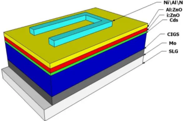
A conventional CIGS solar cell structure and its layers are represented in Figure 1.2.
The usual substrate used for a CIGS solar cell is soda lime glass (SLG). SLG is cheap, thermally stable, has a smooth surface and an expansion coefficient close to the CIGS absorber, this is important due to the high temperatures reached during the CIGS absorber deposition [18]. SLG serves also as a sodium(Na) source, an element that improves the electrical performance of a CIGS solar cell [20].
Sputtered molybdenum(Mo) is used as the rear contact material for CIGS solar cells, due to several reasons; i) high melting point of around 2700 ºC, which allows to survive the harsh growth conditions of the absorber layer and ii)low diffusivity into the semiconductor films [19]. For Mo to achieve a good adhesion to the substrate and also a low resistivity, it is necessary to perform a bi-layer deposition [21]. The first deposition is performed at a high pressure to promote a better adhesion to the substrate surface and the second deposition at low pressure to reduce the film resistivity. One particular feature of Mo is it reaction with selenium [21]. A layer of MoSe2 will form at the interface with CIGS leading to a formation of a quasi-ohmic contact with CIGS [22].
The absorber will be discussed in detail later.
Following the absorber deposition, the formation of the p-n junction is assured with the deposition of a thin n-type buffer layer. Cadmium sulphide (CdS), deposited by chemical bath deposition(CBD) [21]. However, this layer has toxicity problems due to presence of cadmium and since it has a relativity low band-gap (2.4 eV) [19], some parasitic absorption occurs [11].Nonetheless, CdS, transmits most of incoming light to the absorber, it has a favorable band alignment with CIGS and forms a high quality p-n junction [21].
A transparent conducting oxide (TCO) is used for the window layer. The selection of which TCO to use must take into account the following conditions: i) formation of a transparent low resistant contact and at the same time a high resistant element to screen shunts and ii) create a favorable band alignment with the buffer layer [19]. Thus, to satisfy these conditions a by-layer is fundamental, being the first a thin layer with high resistivity, typically intrinsic zinc oxide (i:ZnO), the second layer with low resistivity, aluminium doped zinc oxide(Al:ZnO). Usually both layers are deposited by sputtering [21], however some alternate methods can be used [23], [24]. The i:ZnO will help to prevent any current leakage due to inhomogeneities. The Al:ZnO layer allows for high light transmission at minimum optical absorption [18].
The front contact is a stack of nickel(Ni)/aluminium(Al)/nickel(Ni), usually deposited by evaporation [21]. Depositing Al on top of Al:ZnO will dope the former layer, thus altering its proprieties [25]. Hence, a thin Ni layer is deposited to prevent the diffusion of Al and helps to protect the TCO layer. Since Al has a high malleability, it favors the electrical contact when doing measurements that use probes.
3
1.2.1
State of the art
The story of CIGS began in 1975, at Bell laboratories when scientists achieved a power conversion efficiency value of 12%, by evaporating CdS on top of CuInSe2 single crystal[26].
Research groups, stimulated by the results, began to develop different deposition process. Boeing and Arco solar had different deposition methods that achieved a good power conversion efficiency, Boeing was the first group to present a thin film device with more than 10% of power conversion efficiency, with a co-evaporation process, where Cu, In and Se were deposited from different evaporation sources [27]. Soon after, Arco solar, with a deposition-reaction process where Cu an In acted as metallic precursors and H2Se the reacting chalcogen source, manage to achieved an higher
power conversion efficiency value of 12 % with solar cells produced using the mentioned method. When the three-staged co-evaporation method invented by the National Renewable Energy Laboratories (NREL)[28], in 1994, provided the basis for 20 % in power conversion efficiency for a CIGS solar cell. Currently, this method is the most used deposition method for CIGS solar cells.
The effect of alkali elements on absorber layer has been a continuous research topic among the CIGS community, since it was first reported by Boeing in the 1980s [29]. However, the full effect of such materials in the absorber is not yet fully understood. Nonetheless, CIGS solar cells with a high power conversion efficiency use a three-staged co evaporation and incorporate alkali elements in the absorber layer[30], [31].
1.2.2
CIGS material
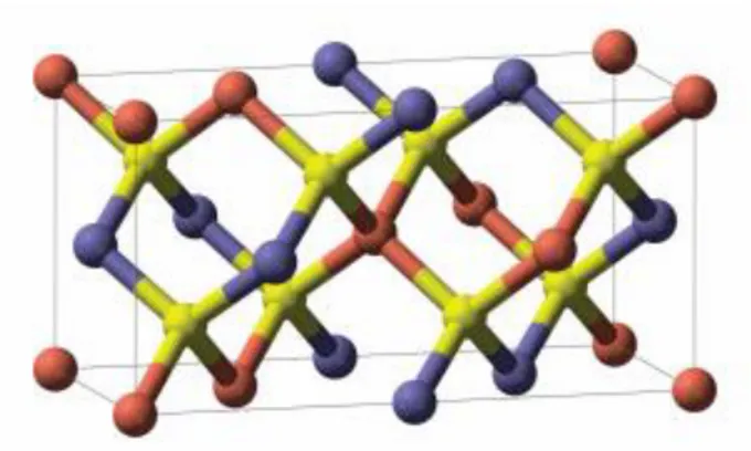
The CIGS compounds belong to the chalcogenide group. Chalcogenide materials are chemical compounds consisting of at least one chalcogen anion, a chemical element in column VI of the periodic table. One group of chalcogenides is the chalcopyrite crystal structure, which forms a tetragonal crystal structure ( Figure 1.3) [32].
Figure 1-3 - The crystal structure of CIGS. The colours indicate copper (red), selenium (yellow) and in-dium (blue). The inin-dium atoms can be replaced be Ga.[31]
Many chalcopyrite materials are semiconductors, of the type I-III-IV [31]. One of the most common chalcopyrite used for solar cells, is a compound containing a mixture of copper indium diselenide (CuInSe2,CIS) and copper gallium diselenide(CuGaSe2,CGS), the compound resulting from
this mixture is called (Cu(InxGa1-x)Se, CIGS), where x can vary from 0 to 1 [15]. These compounds are
4 composition [33].
CIGS is a p-type and direct bandgap semiconductor with a high value of absorption coefficient up to 105cm-1 [19]. This high value of absorption coefficient allows the use of a thin layer(1-3µm) to
achieve the same light absorption as multicristalline silicon which uses a much thicker layer, around 200µm. The electron diffusion length is low but it is in the order of the used thickness of CIGS [34].
CIGS has a self-doping nature, due to Cu vacancies. When it comes to the definition of CIGS properties, its Cu concentration is very crucial. Cu-poor CIGS, defined by the ratio ([Cu]/[Ga]+[In]) <1 , has smaller grains and presents good electrical performance.In contrast, Cu-rich CIGS, defined by the
ratio higher than 1, has bigger grains and good crystalline properties although its electrical performance is weak comparing to the Cu-poor CIGS, caused by lower p-type doping and existence of Cu2−xSe [15],
[35].
One interesting feature of CIGS compound is the ability to tune its bandgap to generate a quasi-electrical field by changing the gallium (Ga) gradient along the thickness of the absorber layer (replacement of In atoms of Ga) thus making its bandgap values range from 1.02 to 1.68eV [19].
1.3
Passivation effect
The major electrical losses that CIGS solar cells have are bulk and interface recombination, limiting the solar performance [10].
A way to reduce the recombination of the rear is by Ga grading [36]. By adjusting the quantity of Ga at the rear, it creates a quasi-electrical field that forces the minority carriers away from the rear thus reducing the recombination.
The interface recombination can be addressed with the introduction of a passivation layer, normally an insulator, at the interfaces. This passivation effect can be split in two: i) chemical passivation, a term originated from the Si technology, this type of passivation decreases the number of active defects at the interface [37]; ii) field-effect passivation, the passivation layer has a high number of fixed charges, which produces a field effect that repels the minority carriers [37].When addressing the recombination at the rear with a passivation layer, an optical effect occurs as the rear optical reflection [37]increases, however this enhancement is insufficient for fully enhancing the light absorption in the CIGS layer [36].
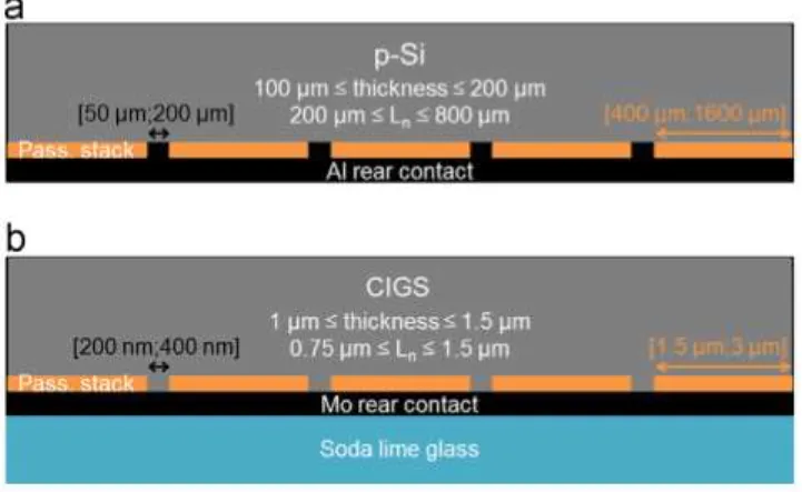
The first mention of the use of a passivation layer alongside with nano-size point contacts was done by Green et al [3] by introducing the so-called Point Passivated Emitter and Rear Contact solar
cell structure (PERC) [3]. In silicon solar cell technology this allowed the increase of the VOC. This
structure is described in Figure 1.4. It allows for a reduction in the rear recombination by decreasing the
contact area between the metal and semiconductor along with the passivation layer.
Figure 1.4 - Schematic representation of the rear of (a) a p-type Si solar cell with a surface passivation stack and micron-sized local point contacts and (b) CIGS solar cell with a surface passivation stack and
5 However, when bring the PERC structure to CIGS solar cells, the diffusion length of the minority carriers has to be taken in to account in order to determine the better dimensions of the point contacts[34].
In a recent study, Salomé et all [37] ,demonstrated, once again [38], the passivation effects of
Al2O3,where the solar cells that incorporate the dielectric showed higher figures of merit than the solar
cell with no dielectric material. Due to the good results achieved, Al2O3, will be used as the dielectric
material on this thesis. Other materials are also being tested as passivation material such as titanium oxide (TiO2)[39], zinc sulfide (ZnS) [40] and some dielectrics materials like hafnium oxide( HfO2) ,
7
2
Materials and methods
The main objective of this work is to increase the optical refection at the rear of a CIGS solar cell, by depositing metals on top of the rear contact and below the dielectric layer. The metals were chosen based on their optical properties as well as their availability at the INL cleanroom deposition systems. Thus, six metals Ag,Au,Cu,Ta, Ti and Zn and two metallic alloys, titanium-tungsten (TiW) and AlSiCu are tested. The dielectric to passivate the interface will be Al2O3 and the nanopatterning will be
defined by e-beam lithography and reactive ion etching(RIE).
The following sub-chapter will focus on the fabrication steps until the absorber growth. The remaining fabrication of the solar cells, a standard baseline process, was done by collaborators at Uppsala University in Sweden. After fabrication, the cells are shipped back to INL for further characterization.
2.1
Solar cell fabrication and deposition techniques
Here at INL, we focus in the modification of the rear structure in a CIGS solar cell, as such in this work the fabrication occurred after the Mo deposition and before the CIGS growth (Figure2.1),
whereas the remaining fabrication of the solar cell was to be done at Uppsala University in Sweden.
Figure 2.1 - Standard step by step fabrication for a CIGS solar cell. In this thesis the fabrication will occur between the Mo deposition and the absorber growth. Not on scale
The rear contact, a 350 nm Mo layer, was deposited at Uppsala University using a DC-sputtering system in a vertical inline MRC 603 tool, with a DC power of 1500 W, on top of 5x5 cm2, 2 mm thick
SLG. Afterwards, the samples are shipped to INL. Upon arrival, all samples went through a cleaning process. The process consisted of consecutive ultrasound baths in acetone (10 minutes), followed by isopropanol (10 minutes) and then di-ionized water (5 min).
8 i) For the deposition of Ag, Au, Cu, Ta, Ti and Zn, a Kenosystec- ultra high vacuum tool (UHV) multitarget confocal sputtering tool is used. The DC power was of 400 W, the base pressure was 1x10⁻⁸ mbar, the deposition pressure was 9.1x10⁻³ mbar;
ii) The metallic alloys, TiW and AlSiCu were deposited using a Metallization Singulus Sputtering tool ,Timaris FTM. The substrate temperature is not intentionally increased, however, due to the proximity to the target, it can reach temperature values as high as 200 ºC, which depends on the deposition time.
After the metals deposition, 18nm of Al2O3 was deposited by RF sputtering using the same tool
for the metallic alloy deposition. This was possible due to the possibility of the tool to operate in DC and RF mode.
To create the desired pattern, e-beam lithography was used, the pattern consists of a square array of 200 nm diameter holes with a pitch of 2µm. The pitch is defined as the inter-distance between the start of two consecutive holes.
The lithography process starts with the coating of the samples with a photoresist (PR) designated by polymethyl methacrylate, commonly called PMMA. A Suss Microtec Gamma Cluster track tool was used to deposit the resist. In this system, the PR must be inserted in a syringe and then manually introduced in the track. The deposition of 430 nm PMMA was done by spin-coating for 1 minute followed by a hard-bake at 150 ºC for 1 minute. The samples are exposed using electron-beam lithography system, Vistec 5200 ES 100 with a beam current of 96 nA and an acceleration voltage of 100 kV. Such exposure is very time-consuming, as the exposure for 1 sample takes ~12 hours to complete. After the exposure, the samples were developed. The development is done with a Suss track, the developer used is Methyl isobutyl ketone
(
MIBK) and the each sample development takes 40 seconds.Afterwards, to create nano-sized point contacts a reactive ion etching (RIE) is done through the resist, the dielectric and the metal, using a SPTS ICP system who relies in chlorine ions to etch through the materials. The etching was done for 45 seconds, for all samples that went through the lithography process, a helium gas is used for aiding the backside cooling of the sample. After the etching, the samples were risen with water to prevent any further etching of chlorine ions.
Finally, to remove the unexposed resist, the samples were bathed in acetone and left at the ultrasounds for 20 minutes. After that, the procedure is repeated using deionized water for 5 minutes.
Figure 2.2a) shows the structure before the absorber deposition and in Figure 2.2b) a schematic
9 Figure 2.2 - a) Representation of the structure obtained after the resist removal; b) Schematic showing the fabrication steps. Both figures are not on scale
The samples are then shipped to Uppsala to complete the solar cells fabrication, following the Angstrom solar cell baseline [21]. A CIGS layer was co-evaporated at 550 ºC. A Ga flat gradient was used to prevent a Cu and Ga depth profile. The composition of the CIGS is: [Cu]/[Ga]+[In] = 0.90 and [Ga]/[Ga] + [In] = 0.30.
Thirteen sets of solar cells were then made, where two sets are regular CIGS solar cells, designated as reference with a structure: Mo\CIGS\CdS\i:ZnO\Al:ZnO\Ni/Al/Ni grid, two sets incorporate Al2O3 with the following structure: Mo\Al2O3\CIGS\CdS\i:ZnO\Al:ZnO\Ni/Al/Ni grid. The
remaining eleven sets will use the metal layer as well as Al2O3, with the following structure:
Mo\Metal\Al2O3\CIGS\CdS\i:ZnO\Al:ZnO\Ni/Al/Ni grid. The sample names as well the summarized
information is found in Table 1.
Table 1 - Summarized information of the samples produced in this work as well as their naming
Pitch: 2 µm; Hole diameter:200 nm; Al2O3 thickness:18 nm; Metal thickness: 20 nm
Metal Number of samples Sample name
Only with Al2O3 2 Mo/Al2O3-I; Mo/Al2O3 -II
TiW 2 Mo/TiW/Al2O3-I; Mo/TiW/Al2O3 -II
Au 1 Mo/Au/Al2O3
AlSiCu 1 Mo/AlSiCu/Al2O3
Ta 1 Mo/Ta/Al2O3
Ti 1 Mo/Ti/Al2O3
Zn 1 Mo/Zn/Al2O3
Cu 1 Mo/Cu/Al2O3
Ag 1 Mo/Ag/Al2O3
Reference samples 2 Reference -I; Reference -II
2.2
Characterization techniques
In this section, the characterization techniques used in this work are described. The samples are characterized at two stages in their production. Before the CIGS deposition, the surface is characterized and the samples relative optical reflection is measured. After complete solar cell processing, the cells were characterized by J-V, EQE and relative optical reflection measurements.
10 NovaNanoSEM650 system was used, with an acceleration voltage of 5kV.
Morphology analysis was done using Atomic Force Microscopy (AFM), on tapping mode and with a scan rate of 1Hz in the system AFM Dimension Icon.
To measure the relative optical reflection UV-VIS NIR Spectrophotometer was used using an integrating sphere. The wavelength range used was from 300 to 1100 nm with a step of 10 nm.
The J-V measurements were performed in Uppsala university, using a home-made J-V system. Where a tungsten halogen lamp was used. The lamp was calibrated, with a certified silicon photodiode
from Hamamatsu Photonics to give the same amount of photon as in AM1.5 light with an intensity of 1kW/m2. The voltage range was from -0.5 V to 1 V with a step of 50 mV.
EQE measurements, done at INL, were performed using a solar cell efficiency measurement system QEX10, with a monochromatic light scanned trough the wavelength interval of 300 nm to 1100 nm with a step of 10 nm.
The optical simulations were done employing 3D a Finite-Difference Time domain (FDTD) using a commercial software Lumerical.
This method solves Maxwell’s curl equations in arbitrary geometries and materials. The equations are the following [42]:
𝜕𝑫 𝜕𝑡 = ∇ 𝑯
(5)
𝜕𝑫 𝜕𝑡 = ∇ 𝑯
(6)
𝜕𝑯 𝜕𝑡 = −
1 µ𝑜 ∇ 𝑬
(7)
where H,D and E are the magnetic, displacement and electric fields, respectively, while 𝜖𝛾(𝜔) is the
complex relative dielectric constant (𝜖𝛾(𝜔) = 𝑛2, where n is the refractive index).
Due to the periodicity of the square array of rear point contacts,2µm pitch, we can reduce the FDTD region to a square unit cell with a 2μm side. Specific boundary conditions (BCs) were applied in each face of such region. Artificial absorbing perfect-matching layers were applied on the upper and lower boundaries to absorb all outgoing waves. On the side boundaries, periodic BCs were used to model the infinite periodicity of the structures. Here, due to the symmetries of the structure at normal incidence, symmetric and antisymmetric BCs were employed, which allow simulating only one quadrant of the unit cell.
11
3
Results and discussion
In this chapter, each result will be shown and discussed.
First, to analyse the optimum optical behaviour of the solar cells produced in this work as well as the optical influence of the metal layer, optical simulations were conducted using the commercial software Lumerical and its results are presented and discussed.
The samples are analysed by SEM images, prior the absorber growth to ensure that the hole diameter has the expected dimension and the optical relative reflectance was also measured.
The solar cells are then analysed by optical relative reflectance, J-V and EQE measurements.
3.1
Numerical model
The optical properties of the materials utilized in our structures are determined by the values of complex refractive index(n,k). For the materials, Au,Ag,Cu,Al2O3 and Ti , the complex refractive index
values were taken from ref [43], for Ta and Zn the values were taken from ref [44] , for AlSiCu it was from ref [45] the values for CIGS with [Ga/(Ga+In)] =0.30 were taken from ref [46].Unfortunately, the optical ellipsometry results for TiW did not arrive in time to be included in the optical simulations.
The power absorbed per unit volume (PABS) in each element of the structure used in the optical
simulations is given be the resulting electric field distribution established in their material:
𝑃𝐴𝐵𝑆 =12 ⍵є′′|𝑬|𝟐 (7)
where, 𝜔, is the light angular frequency,є′′ is the imaginary part of the dielectric permittivity and |𝑬|𝟐 is the electrical field intensity. PABS is normalized by the source power to obtain the absorption per unit
volume, pABS. The total light absorption in a region, at a certain wavelength(λ) is computed by integrating
pABS over its volume:
𝐴𝑏𝑠(𝜆) = ∫ 𝑝𝐴𝐵𝑆𝑑𝑉 (8)
In the solar cells produced in this work, only light absorbed in the CIGS layer leads to photocurrent. Thus, in the simulations we integrate pABS, only in this layer, since light absorbed in the
other layers leads to parasitic absorption resulting in optical losses. Trough, the integration of pABS on
the CIGS layer and the assumption that every photon absorbed in the CIGS layer generates carriers, the software can calculate JSC values. Hence, JSC values are determined integrating the absorption in the
CIGS layer with the incident AM1.5 solar power spectrum, over the desired wavelength range (300-1100 nm):
𝐽𝑆𝐶= 𝑞 ∫ℎ𝑐 𝐴𝑏𝑠𝜆 (𝜆)𝐼𝐴𝑀1.5(𝜆)𝑑(𝜆) (9)
where, q is the electronic charge, h is the Planck constant and c is the free space light speed. The
wavelength interval was chosen between these values as light outside this interval does not contribute to the photo-generated current: light with energy higher than 300 nm is absorbed in the windows layers; light with energy below 1100 nm is below the bandgap of the CIGS used in this work ,1.2 eV. The determination of the CIGS bandgap is shown in Annex A. The JSC values calculated can be regarded as
optimal, as it does not consider any electrical losses or other experimental situations such as: roughness, interfaces, elemental diffusion, light scattering at grain boundaries, among others. For a more detailed description on the numerical methods, the reader is pointed to refs [42], [47], [48].
The optical simulations conducted in this thesis, are presented in the following sub-chapters. We will start with the identification of optical losses in ultrathin CIGS layer by comparison with a thick counter-part. Then, a solution to address these losses is presented and discussed.
12 the Transfer Matrix analytical formalism. If both plots overlap the simulation has a good precision level. This comparison is seen in Figure 6.2. For simplicity, only one plot is shown as all present simulations
present qualitatively good overlaps.
3.1.1
Optical characteristics with ultrathin absorber
In this section, we compare the optical characteristics of our 500 nm absorber ultrathin reference solar cell with a 500 nm absorber with a standard-thick solar cell possessing a 2 µm thick CIGS layer. In the simulations, the only difference between the cells is the absorber thickness, the remaining layers have the same thickness value.
The simulations results are present in Figure 3.1a,b), where the CIGS, solar cell absorption,
reflectance and Mo parasitic light absorption of the simulated solar cells are shown, and the results are summarized in Table 2. Henceforth, when the author mentions reflection it regards only the optical
reflection, any other form of reflection will be properly identified. Ultrathin devices have high optical losses due to a low absorption values for wavelengths higher than 600 nm as verified experimentally [10]. This is clear in Figure 3.1a), as the light absorptance for the ultrathin solar cell decays very fast
for the wavelength mentioned above. The optimal JSC, discarding any electrical losses, for the 2µm solar
is 33.85 mA/cm2 and for the ultrathin solar cell 30.03 mA/cm2. Thus, the difference between the absorber
layers thickness is responsible for a 3.82mA/cm2 optical loss. Note once again, that this difference only
accounts for optical considerations, excluding electronic ones which are responsible for significant losses as well [10], [37]. It should also be noted that the thick solar cell is relatively simple compared with the CIGS state-of-the-art cells that present Ga values dependent on depth and several front interface modifications that heavily change the absorption properties. Such aspects explain the lower value of the simulations compared with the world-record values (~36 mA/ cm2) [6].Furthermore, from Figure 3.1b),
the solar cells reflectance differs for wavelength value higher than 1000 nm, with the standard-thick solar cell with 2 µm CIGS having a poor reflectance. This is due to: i) the solar cell stack does not reflect much of the incident light since the refractive index gradient of the materials present in the solar cell stack are beneficial for anti-reflective properties [49]; ii)the absorber being thick enough to absorb the incoming light and no losses occur due to reflection of the rear contact. For an ultrathin solar cell, when the light absorption in the CIGS layer decreases, the parasitic absorptance at the rear contact increases. Indicating that most of the light that reaches the rear is absorbed by the contact. Such optical loss was already reported in the literature [10], [14]. The parasitic light absorption at the rear contact is also present for a regular solar cell, however due to the thickness of the absorber only a small fraction is absorbed .According with our simulations, 2.42 mA/cm2 is absorbed at the rear for an ultrathin solar
CIGS solar cell and 0.25 mA/cm2 for a regular CIGS solar cell, these values matches with the ones
simulated by Orgassa et all [14].
A possible solution to decrease such optical loss and enhancing the rear reflection, is proposed in this work, with the simulations results of the proposed solution being presented in the next section.
Figure 3-1 - a) simulated CIGS absorptance for an ultrathin solar cell and a regular solar cell with a 2µm absorbed layer (solid lines), parasitic light absorptance at the rear contact ( dashed lines); b) simulated solar cell reflectance for ultrathin solar cell and a regular solar cell with a 2µm absorbed layer. The calculated JSC for the
13
3.1.2
Simulations for solutions of increasing the rear reflection at
the rear contact
In the previous section the parasitic light absorption at the rear was identified as the main optical loss of an ultrathin solar cell. Thus, this section will focus on a modification to the solar cell architecture that could address this issue. A metallic layer will be incorporated between the rear contact and the dielectric material (Al2O3). The simulation is done using the solar cells structures fabricated in this work.
The simulation results are shown in Figure 3.2, and the JSC values calculated are represented in Table
2. All solar cells that incorporate a metal layer at the rear, show an enhancement in the CIGS light
absorptance for wavelengths higher than 600 nm, over the reference solar cell, with the solar cell with no metal layer giving the worse CIGS light absorptance as seen in Figure 3.2.a). The increase in the
amount of light absorbed at the CIGS layer is due to the poor optical reflectivity of the rear metal (Mo). The enhancement is higher for solar cells that incorporate lower refractive index metals (Figure 6.3), as
such the Mo/Ag/Al2O3 solar cell shows the highest enhancement in light absorptance at the CIGS layer
and with an optimal JSC of 32.05 mA/cm2.Only the solar cell Mo/Ti/Al2O3 gives the lowest JSC valueof
the solar cells simulated with a metal layer, 31.01 mA/cm2. The J
SC values for the Mo/Ti/Al2O3 solar cell
is in fact lower than the one of the Mo/Al2O3 solar cell, 31.15 mA/cm2. The three solar cells,
Mo/Ag/Al2O3, Mo/Au/Al2O3 and Mo/Cu/Al2O3, show the highest enhancement of light absorptance in
the CIGS layer compared with the reference solar cell, being very promising as they increase the JSC
from the reference solar cell from 30.03 to 32.05 mA/cm2, 31.98 mA/cm2, 31.95 mA/cm2, respectively.
Simulations were conducted to study the influence of the metal layer on the parasitic light absorptance at the rear. Hence, we simulated the absorptance at the rear (Mo+Metal), assuming no absorptance in the dielectric layer, with the results shown in Figure 3.2b). Considering this simulation, the solar cell
Mo/Ti/Al2O3 has a parasitic light absorptance, similar to the reference solar cell. Such absorption is due
to the fact that 20 nm of Ti are enough to enhance the parasitic light absorptance and degrading the optical properties of the solar cell. The parasitic light absorptance in this solar cell is responsible for a loss of 2.22 mA/cm2. Apart from Mo/Ti/Al
2O3 solar cell, all of the combinations show a significant
reduction in the parasitic light absorptance at rear contact. Even the simple introduction of the dielectric layer diminishes this losses, which was already confirmed experimentally [37], [38]. From Figure3.2a)
we see that the increase in the light absorptance in the CIGS layer does not correspond to the increase in reflectance for the same wavelength regions, thus some of reflected light leaves the solar cell rather than being absorbed in the CIGS layer as shown by an increase of the reflectance at the wavelength values above 900 nm as seen in Figure 3.2c).
14 Figure 3.2 a) CIGS absorptance for all solar cells simulated; b) total solar cell reflectance for the solar cells simulated; c) parasitic light absorptance at the rear contact for the simulated solar cells.
One additional study done in these simulations, was to compare the performance of the solar cells with the highest light absorptance ,Mo/Ag/Al2O3, with the regular solar cell, as presented in Figure
3.3.The light absorbed in the CIGS layer in the Mo/Ag/Al2O3 surpasses the regular solar cell for certain
wavelengths( ~700 and 800 nm), however for wavelengths higher than 900 nm the Mo/Ag/Al2O3 starts
to underperform. This loss accounts for a difference of 1.3 mA/cm2 in the J
SC between the solar cells.
Such current loss is due to light reflected at the rear leaving the solar cell, hence, to reach the JSC values
of a regular solar cell, light trapping schemes should be also used to promote a longer light path [50], [51]. However, if these reflectance values can be reached with a CIGS thickness reduction of 75% (from 2000 to 500 nm) without compromising on the other figures of merit of the solar cell, a significant cost reduction in the solar cell production could already be achieved. Nonetheless, these simulations assume that the metals survive the harsh CIGS growth conditions, unfortunately, some of these metals are known to easily react with the CIGS and with Se [12]–[14]. Therefore, the technical capability of producing these architectures needs to be experimentally tested.
15 Table 2 - Simulated JSC for all solar cells simulated as well as the JSC absorbed at the rear contact
3.2
Sample fabrication
To increase the rear reflection of an ultrathin CIGS solar cell, the standard rear structure of such solar cell must be modified. Thus, in this work, a metallic layer, 20 nm, is deposited on top of the rear contact, Mo and below the dielectric layer, 18nm of Al2O3 is used. To establish, contact between the
CIGS layer and the rear contact, a pattern consisting of a square array of 200 nm holes with a pitch of 2µm is created by e-beam lithography. RIE is then used for opening the point-contacts. For more detailed information of the solar cells fabrication used in this work, the reader is directed to Section 2.1.
The following section will focus on the characterization of the fabricated samples, before the CIGS growth. Top view SEM images were taken to verify if the point-contacts were successfully open and relative reflection measurements were conducted to verify the samples reflectance.
3.2.1
Substrate characterization
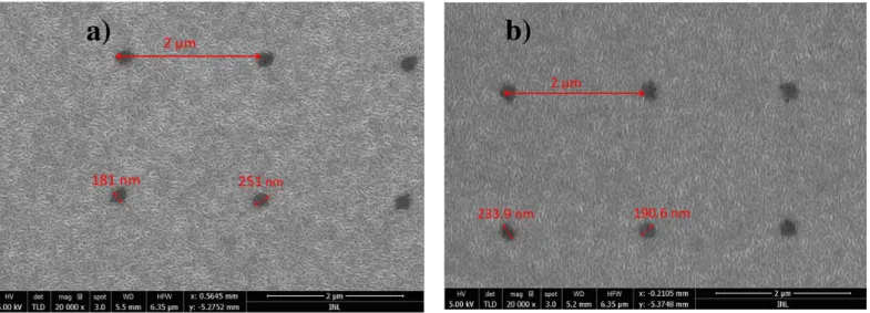
To verify if the e-beam exposure and the etching steps were successful in the formation of the point-contacts, top view SEM images were taken of all the samples, as shown in Figure 3.4. For
simplicity, only the images for samples Mo/Al2O3 and Mo/TiW/Al2O3 are shown, as the desired pattern
was obtained in all samples. The application of e-beam lithography was able to generate the point-contacts on the Al2O3(18nm)and the metal layer (20 nm). All samples have the expected pitch of 2μm,
however, we note that the holes form an elliptical shape rather than circular, causing the dimensions to be elongated in a particular direction. The modification in the holes form as well as in their dimension is attributed to an imperfection in the electron optics, in particular, astigmatism, that occurs in the exposure, leading to an elongation in a privileged direction. However, the e-beam process, could form point-contacts more cylindrical with a higher exposure time. Since, a 5x5 cm2 already takes 12 hours to
expose, we need to compromise exposure time with the point-contacts shape. The dimensions obtained do not make a constraint in the solar cell performance [37]
Simulated solar cell Colour in the plot
JSC given by the optical
simulation (mA/cm2)
Parasitic light absorption at the rear (Mo+Metal)
(mA/cm2)
Reference 30.03 2.42
Mo/Al2O3 31.15 1.30
Mo/Ag/Al2O3 32.01 0.51
Mo/AlSiCu/Al2O3 31.85 0.57
Mo/Au/Al2O3 31.98 0.49
Mo/Cu/Al2O3 31.95 0.59
Mo/Ti/Al2O3 31.01 2.22
Mo/Ta/Al2O3 31.60 1.10
16
Figure 3.4 -SEM top-view images of the samples Mo/Al2O3 (a) and Mo/TiW/Al2O3 (b). The images show the pitch dimensions as well as the hole diameter. A expected 2μm pitch is achieved, the hole diameter is elongated in a particular direction due to e-beam astigmatism.
In Section 3.1 we identified that the poor reflection of the rear contact material as the main
optical loss in an ultrathin CIGS solar cell. Hence, relative reflectance measurements were done to evaluate the reflectance of the samples prior to the absorber growth (Figure 3.5). The samples
Mo/Ag/Al2O3, Mo/Au/Al2O3,and Mo/AlSiCu/Al2O3 present the highest reflectance values for
wavelengths higher than 800 nm and, on the other hand, Mo/Ti/Al2O3 andMo/Ta/Al2O3 having the
lowest reflectance in the same wavelength region. We should note that the interface: Al2O3/air is very
different from Al2O3/CIGS due to a higher refractive index of the absorber material. Hence, interfaces
with the refractive index(Figure 5.3) closer to the refractive index of air ( n=1), present the lowest
reflectance in this measurement.
From these measurements, the samples Mo/Ag/Al2O3, Mo/Au/Al2O3 and Mo/AlSiCu/Al2O3
show the best results in the reflective reflectance, however these metals are known to react very easily with CIGS and Se [12]–[14]. The sample Mo/TiW/Al2O3, shows the most promising results: i) this metal
was tested as back contact for CZTS solar cell, with significant results [52];ii) has high relative reflectance and iii) is stable at high temperatures [53], [54].
17
Figure 3.5 - Measured reflectance of all the samples fabricated prior to the absorber growth. A kink is observed at around 900 nm, due to a change in the detector in the system. Reflectance relative to a BaSO4 refer-ence.
3.3
Solar cells characterization
Upon arrival at Uppsala University, the samples are cut in two pieces of 2.5x5 cm2, to
compensate for any mistakes that could occur during the solar cell processing.
Three samples did not survive the complete solar cells process; the CIGS layer in Mo/TiW/Al2O3, suffered a partial peel-off during the CdS deposition, however, this occurrence might
be linked with high NaF thickness [55]; in Mo/AlSiCu/Al2O3 sample, during the CBD, particles
agglomerated on the sample surface, something that is not yet understood. Still, the solar cells fabrication was successful on the remaining 13 samples, with the results being shown and discussed in the following section. Each sample produced 16 solar cells, with an area of 0.5 cm2 per solar cell.
3.3.1
Solar cells relative reflectance
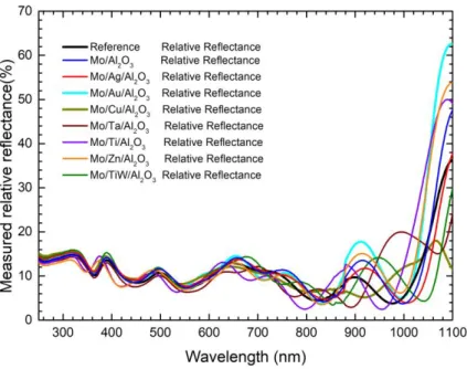
The relative reflectance of the solar cells fabricated is shown in Figure 3.6.
From Figure 3.6 we note that of the samples that showed the highest reflectance in Figure 3.5
(Mo/Au/Al2O3, Mo/Ag/Al2O3, and Mo/Cu/Al2O3), only the sample Mo/Au/Al2O3 has a relative
reflectance higher than the reference solar cell, indicating remarkable differences in the solar cell stack that appeared during the experimental fabrication. The Mo/Ag/Al2O3 solar cell shows a similar
compared to the reference solar cell. For the Mo/Cu/Al2O3, the reflectance is only higher than the
reference solar cell for the wavelength interval between 800 and 900 nm. The difference in the relative reflectance of the solar cells with the corresponding samples reflectance could be an indication of diffusion of such metals (Ag,Cu) to the CIGS. This changes the rear layers uniformity, affecting the reflectance. The relative reflectance of the solar cells Mo/Al2O3 and Mo/Zn/Al2O3 is higher than of the
18 Mo/Ti/Al2O3 shows the second highest reflectance, which does not match the simulated reflectance of
such solar cell. The difference could be attributed to the reaction of titanium with Se, forming TiSe2 [56]
a compound with high reflectivity for wavelengths higher than 900 nm [56], possibly explaining the difference between the simulated and measured reflectance for this solar cell.
Figure 3-6– Measured relative reflectance of the solar cells fabricated.
3.3.2
Electrical characterization
J-V and EQE measurements were done for the solar cells that survived the fabrication process, with the representative illuminated J-V curves being shown in Figure 3.7a),b). In figure 3.7a) the
samples that showed no diode like behaviour are shown, whereas, Figure 3.7b) shows the samples with
a good diode like behaviour. The J-V curves presented are representative. Henceforth, when the author
mentions the figure of merit values for the solar cells it refers to the average values for each sample. The EQE spectra is shown in Figure 3.7c). From the measurements, the solar cells figure of merit were
extracted and the average values as well as their standard deviation are shown in Table 3. From the EQE
curves, it is possible to extract the JSC employing the following equation [19] :
JSC =𝑞 ∫ ф(𝜆)𝐸𝑄𝐸(𝜆)𝑑𝜆 (10)
where q, is the electron charge, ф is the photon flux.
The reference sample showed power conversion efficiency values of 6.17%, and a VOC of 552
mV. The VOC of the reference sample is being limited by rear interface recombination, as ultrathin CIGS
solar cells are known to have a high rear interface recombination [34], [37]. By analysing the J-V curve for this sample (Figure3.7b), we note a slope on the 3rd quadrant. The slope is an indication of shunts,
which is confirmed by a dark measurement (Figure 6.4a), as the same behaviour is present. The
difference in the JSC values from the simulated reference sample (30.3 mA/cm2) with the measured
reference sample,23.23 mA/cm2, is attributed to electrical losses, namely the high interface
recombination which is associated with these devices and other losses which are not accounted by the pure optical model (grain boundaries, bulk recombination, band misalignments, etc.) [37]. There is a 1.86 mA/cm2 J
SC difference between the measured by J-V JSC and the JSC calculated trough EQE, 21.37
mA/cm2. Such difference is linked with the existing shunts in the reference sample [19]. As only a small
area is illuminated when doing the EQE measurement, the generated carriers can diffuse trough shunt paths in the non-illuminated area, lowering the EQE values. The introduction of the passivation layer, Al2O3, increases the solar cell figures of merit when comparing with the reference sample and reduces
19 5.6 %, resulting in 1.5% enhancement on the efficiency value. The measured J-V JSC enhancement is
bigger than the simulated JSC enhancement of 0.85 mA/cm2. Such difference indicates the electrical
effects, not taken in consideration in the optical model, gained by the passivation layer are responsible for the enhancement [37], [38]. However, the VOC enhancement (558 mV vs 553 mV) is rather low for
the values reported in the literature [37], [38]. The reason for such small enhancement is the “roll-over”
seen in the illuminated J-V curve. Such behaviour is common in devices that have insufficient Na in the CIGS layer. [20], [57]. The presence of Na in a CIGS solar cell is known to enhance its electrical properties, as it increases the free carrier concentration by decreasing the electrically active donors [20], [55]. Although the exact physical mechanism for which it happens is still debated [58], [59]. Due to the blocking properties of Al2O3, Na is introduced in the solar cell by a NaF precursor layer, deposited before
the CIGS. The optimal NaF thickness for an ultrathin CIGS solar cell has not yet been found. We attribute the insufficient Na in this solar cell to a lower NaF thickness than deposited, the deviation comes from an imprecise control on the NaF evaporation process. Hence, due to insufficient Na this solar cell suffers from low VOC values. Consequently, while a fair comparison would be done with an
optimum amount of Na, this study alone shows already an additional complexity of the ultrathin approach: ultrathin CIGS layers are much more sensitive to Na contents that thick CIGS layers [55].
The samples that incorporate the metallic layer shows very diverse results, hence we will start by comparing them in terms of efficiency values. The samples which showed the best optical performance in Section 3.1 ,Mo/Au/Al2O3, Mo/Ag/Al2O3, and Mo/Cu/Al2O3, after the fabrication show
extremely low efficiency values, 1.2 %, 2.4 %, 0.04% respectively. The reasons for such low performance will be discussed further below. The samples Mo/Ta/Al2O3, and Mo/Ti/Al2O3 have
efficiency values (1.22 %, 3.98%) lower than the reference samples. The Mo/Zn/Al2O3 sampleachieved
an efficiency value of 7.13 %, having a 0.38 % enhancement over reference sample. One remarkable samples are the ones that incorporate TiW (Mo/TiW/Al2O3 -I and II). They achieved efficiency values
of 9.86 % for Mo/TiW/Al2O3– I, and 8.86% for Mo/TiW/Al2O3-II, with an increase of 3.69% and 1.96
% respectively over the reference sample.
The illuminated J-V curves for the sample Mo/Cu/Al2O3 (Figure 3.7a)show that this sample is
completely shunted. The shunting can occur due to Cu diffusion to the absorber during its growth, changing the CIGS properties. The worst case, like the one seen here, would be the formation of CIGS Cu-rich which is very conductive [33] hence, easily forming shunts paths. Thus, this sample figures of merit are negligible: a VOC of 2 mV and the JSC being 1.34 mA/cm2, neither FF nor efficiency values
could be extracted from this sample. During the CdS deposition, particles agglomerated at the Mo/AlSiCu/Al2O3 sample surface, hence affecting its current transport, as the carriers are not able to be
collected by the front contact, as seen in the illuminated J-V curve(Figure 3.7a). Therefore, this sample
figures of merit are heavily affected by this undesirable effect, having a JSC of 0.47 mA/cm2, VOC of 404
mVand an efficiency value of only 0.04 %. At this point, the reason why a rear metal would influence the top CdS deposition is unknown and very hard to interpret with no similar results in the literature, however, it is known that Al diffuses even better than Cu in CIGS which could lead to a different CIGS morphology leading to a different CdS chemical bath deposition. The, Mo/Ag/Al2O3 (Figure 3.7b)
sample, has a slope in the 3rd quadrant in the illuminated J-V curve, which could indicate shunting
problems, however the dark J-V curve shows no sign of shunting (Figure 6.4c). Hence, this sample is
being affected by voltage-dependent current collection(VDCC)[18], [37]. VDCC occurs in a device with a low effective diffusion length and neglectable loss in the space charge region [18], [37]. In these conditions a small change in the voltage will change the space charge region affecting the current collection of such devices leading to significant changes in the JSC. We attribute the VDCC to high rear
interface recombination present in this solar cell [18], [37]. As such, the sample figures of merits are being very limited by the high rear interface recombination with a VOC value of 304 mV and the JSC of
15.43 mA/cm2
. When the solar cell scribing was done, at Uppsala University, problems arise, resulting
in some solar cells within the sample having an lower area than defined, resulting in non-trustful JSC
values. Such low figures of merit for this sample is attributed to and uncontrolled Ag diffusion to the absorber, leading to additional defects in the CIGS layer [60], [61]. The sample Mo/Au/Al2O3(Figure3.7a) has the same behaviour as the Mo/Cu/Al2O3 (Figure 3.7a). However the
Mo/Au/Al2O3 sample is still able to generate photocurrent, with JSC values of 22.19 mA/cm2. The VOC of