U
NIVERSIDADE DO
A
LGARVE
Faculdade de Ciências e Tecnologia
Design and implementation of microstrip filters
for a radio over fiber network demonstrator
Paulo Roberto Ferreira da Rocha
Master in Electrical Engineer and Telecommunications
U
NIVERSIDADE DO
A
LGARVE
Faculdade de Ciências e Tecnologia
Design and implementation of microstrip filters
for a radio over fiber network demonstrator
Paulo Roberto Ferreira da Rocha
Supervisor:
Professora Doutora Maria do Carmo Raposo de Medeiros
Master in Electrical Engineer and Telecommunications
i
Declaration
Paulo Roberto Ferreira da Rocha, Universidade do Algarve student declares that he is the author of this master dissertation.
Student:
Paulo Roberto Ferreira da Rocha
Supervisor:
Professora Doutora Maria do Carmo Raposo de Medeiros
iii
Abstract
The need for networks able of integrating services such as voice, video, data and mobility is growing. To satisfy such needs wireless networks with a high data transmission capacity are required.
An efficient solution for these broadband wireless networks is to transmit radio signals to the Base Stations (BS) via optical fiber using Wavelength Division Multiplexing (WDM). The WDM usage helps this growing, allowing the use of a single optical fiber to feed several BSs using for each one a different wavelength (or WDM channel). Additionally, in the RoFnet project in order to improve radio coverage within a cell, it is considered a sectorized antenna interface. The combination of subcarrier multiplexing (SCM) with WDM, further simplifies the network architecture, by using a specific wavelength channel to feed an individual BS and different subcarriers to drive the individual antenna sectors within the BS.
This dissertation reports the design and simulation of the microstrip bandpass filters used at the BS on of the RoFnet demonstrator. These bandpass filters are used for the filtering of fours subcarrier multiplexed channels located at (9, 11, 13, 15 and 17 GHz). The design and simulation of the lowpass root raised cosine filter required for testing is also discussed. Additionally, the design and testing of two power splitter is reported. Finally, all the designed components were brought together and the overall BS performance is assessed.
The microstrip components have been designed and simulated using both ADS (Agilent’s Advanced Design System) and Momentum simulators.
Kewords: microstrip filter, lowpass filter, bandpass filter, power divider, power combiner, Wilkinson power divider, Radio over Fiber and Advanced Design System.
v
Resumo
Sistemas de Rádio sobre Fibra (RoF - Radio over Fiber) que operam na gama de frequências milimétricas (mm-wave), apresentam muitas vantagens para a implementação de sistemas de acesso das redes sem fios. No entanto, devido às suas características de propagação estes sistemas apresentam tamanhos de células pequenos e consequentemente necessitam de um grande número de estações base (BS-Base Station) para cobrir uma determinada área geográfica. Uma rede RoF, é composta por várias BSs ligadas a uma estação central (CO-Central Office) por uma rede de acesso de fibra óptica. Dentro de cada BS o sinal necessita de ser filtrado através de filtros passa banda e formatado através do filtro passa baixo Raised-Cosine, na banda base de modo a minimizar a interferência inter-simbólica na transmissão dos sinais. Divisores de potência também são considerados na arquitectura proposta para a BS.
Nesta dissertação é apresentada a implementação dos componentes necessários á tecnologia Rádio sobre Fibra utilizando a tecnologia microstrip. Esta tecnologia consiste num condutor assente num substrato com um respectivo dieléctrico e é usada para construir antenas, acopladores, filtros e divisores de potência a um preço reduzido quando comparado aos componentes que operam na gama de frequências tradicional. Outras vantagens são a reduzida dimensão dos componentes assim como o seu baixo custo. Por outro lado, são dispositivos com facilidade de perda de potência e muito susceptíveis a radiações e/ou efeitos electromagnéticos entre as linhas de transmissão adjacentes e o substrato em que assentam.
A implementação dos componentes do projecto é feita no software Advanced Design System (ADS). Este software incorpora ferramentas de simulação bastante úteis para a análise dos componentes implementados neste mestrado. O Momentum é um simulador determinante na construção de dispositivos em microstrip devido á densidade de efeitos electromagnéticos ao longo das linhas de transmissão. Esta ferramenta identifica efeitos de coupling, produz resultados próximos da realidade e permite visualizar radiações e variações de corrente no circuito.
Os filtros têm como objectivo obter uma determinada largura de banda, atenuando todas as frequências fora deste intervalo. Na banda passante do filtro idealmente não existe atenuação e no intervalo rejeitado a atenuação será máxima. No caso dos condensadores,
vi
bobines e linhas de transmissão a atenuação na banda passante está sempre presente. Esta atenuação só pode ser melhorada pela escolha correcta dos componentes do filtro, minimizando assim a atenuação na banda passante e melhorando a eficácia de filtragem. Em baixas frequências, os condensadores e bobines são usados para o desenho dos filtros. No entanto, em altas frequências o uso de secções de linhas de transmissão que têm um funcionamento equivalente ao dos condensadores e bobines é mais o método de desenho mais habitual, ou seja microstrip.
As técnicas utilizadas para o desenho dos filtros podem ser Image Parameter Method ou Insertion loss Method. Image Parameter Method tem a desvantagem de não se poder controlar a resposta na banda passante e na banda de rejeição. O segundo método começa com um protótipo de filtros passa baixo baseado nas curvas de atenuação dos filtros Butteworth ou Chebyshev. A atenuação na banda passante e de rejeição pode ser controlada com base no número de secções de linhas de transmissão escolhido e nas características dos componentes usados tais como a espessura do substrato, do condutor e o dieléctrico do mesmo.
O filtro passa baixo com uma resposta equivalente ao Square Root Raised Cosine (SRRCOS) foi implementado e posteriormente simulado no Momentum no qual não deferiu significativamente. A construção deste tipo de filtros tem como base um filtro passa baixo que consiste em linhas de grande e baixa impedância consecutivamente ligadas entre si. No entanto, para conseguir trazer a resposta para zero como no square root raised cosine filter (SRRCOS) foi utilizado um Open Circuit Stub com um comprimento de 4na frequência do filtro. Este componente é transformado num curto-circuito e a impedância de entrada na direcção do Stub torna-se zero. O curto-circuito à saída do filtro cria o zero pretendido pela resposta do SRRCOS.
A implementação dos filtros passa banda é efectuada recorrendo ao efeito de coupling entre duas linhas de transmissão próximas uma da outra. O método utilizado para implementar os filtros passa banda chama-se parallel coupled lines, e consiste numa cascata de secções de linhas de transmissão contendo cada uma delas duas linhas em paralelo, em que o número de secções determina a ordem do filtro. Esta estrutura é analisada pelo método de simetria Even and Odd mode que consiste em obter os parâmetros-S do componente.
Nas altas frequências os filtros passa banda implementados apresentam bastantes oscilações devido ao facto da construção estar no limite de largura de banda suportada pelo método utilizado, devido aos efeitos de coupling das linhas de transmissão paralelas entre si e
vii devido à necessidade acrescida de processamento nesta gama de frequências. A tecnologia Microstrip apresenta uma limitação na construção de filtros passa banda estreitos. Para este efeito é necessário um grande espaçamento nas linhas de transmissão paralelas entre si, provocando uma maior atenuação na resposta do filtro. Na implementação deste filtro aumentou-se a largura de banda e deslocou-se o filtro para a zona do espectro que não contem informação relevante.
Para dividir o mesmo sinal e obter a mesma potência nas duas saídas normalmente utiliza-se o Wilkinson power divider. Este divisor pode ter uma ou mais secções consoante a largura de banda pretendida e tamanho disponível no substrato. A sua análise é também efectuada através do método Even and Odd mode. É usual na construção deste dispositivo a implementação de uma resistência ao longo das diversas secções, para fornecer um melhor isolamento nas portas de saída do divisor. As resistências utilizadas na dissertação chamam-se thin film resistors. A análise do power divider consiste no estudo dos parâmetros-S, mais precisamente na análise de isolamento entre as portas, port matching e insertion loss.
Os divisores de potência foram devidamente implementados e co-simulados no Momentum. Co-simulados pois o Momentum só por si, não considera os elementos físicos de circuitos tais como as resistências. Para este efeito, o componente foi gerado no layout e foram inseridas portas internas no circuito para posteriormente poder-se ligar os componentes. Depois foi gerado um componente com base na arquitectura e importado para o schematic para se poder efectuar a simulação electromagnética com as resistências integradas. O último divisor desenhado em vez de resistências ideais utiliza uma resistência do tipo thin film resistor. Este tipo de resistência, devido à sua constituição foi simulado apenas no Momentum.
Na simulação geral é possível ver todos os elementos desenhados em microstrip em conjunto com os restantes dispositivos presentes na arquitectura deste projecto. Inicialmente é gerada uma sequência aleatória de bits. Estes dados são filtrados e situados no espectro nas frequências 9,11,13,15 e 17 GHz. Posteriormente o sinal é dividido e filtrado pelos primeiros filtros passa banda de banda larga. O sinal é novamente dividido para posteriormente ser filtrado pelos filtros passa banda especificamente desenhados para cada uma das frequências do espectro (9, 11, 13, 15 e 17 GHz). Após este processo é aplicado novamente o filtro Square Root Raised Cosine para se proceder à análise da qualidade de serviço da rede através do
viii
diagrama de olho. Outra análise efectuada é a visualização do espectro de frequências em determinados pontos fulcrais da arquitectura da BS.
Palavras-chave: Filtros em Microstrip, filtros passa baixo, filtros passa banda, divisores de sinal, Wilkinson Power Divider, Radio over Fiber, Advanced Design System.
ix
Acknowledgements
In these years I have benefited a lot from the extensive knowledge and experience of my supervisor Prof. Maria Carmo Raposo de Medeiros. It has been pleasure learning from her and being motivated by her.
This work could not be achieved without the precious help and guidance of Prof. Izzat Darwazeh. His excellent support and work methodology were fundamental for the accomplishment of this dissertation.
Special thanks to my parents João Rocha and Neyde Rocha who always supported me, my girlfriend Ida Gaspar, my friends Mark Guerreiro, Ricardo Avó, José Coimbra and Hélio Vargues. Their help was very important for the accomplishment of this project.
xi
Table of contents
Declaration... i Abstract ... iii Resumo ... v Acknowledgements ... ix Table of contents ... xi List of figures ... xv Abbreviations ... xix 1. Introduction ... 1 1.1. Introduction ... 1 1.2. RoFnet Project ... 2 1.3. Downlink operation ... 2 1.4. Uplink Operation ... 3 1.5. Dissertation Goals ... 4 1.6. Dissertation Organization ... 4 2. Theoretical fundaments ... 7 2.1. Introduction ... 7 2.2. Microwave ... 7 2.3. Transmission lines ... 7 2.3.1. Propagation ... 92.3.2. Microstrip transmission lines ... 10
xii 2.3.4. Discontinuities ... 19 2.3.5. Stub tuning ... 21 2.4. Scattering Matrix ... 21 2.5. ABCD parameters ... 22 2.6. Richard’s Transformation... 23 2.7. Kurodas’s Identities ... 25 2.8. Digital transmission ... 26
2.8.1. Digital transmission trough band limited channels ... 26
2.8.2. Nyquist criteria for zero ISI ... 26
2.8.3. Raised Cosine shaping ... 27
2.9. Chapter Summary ... 29
3. Lowpass and bandpass filtering ... 31
3.1. Introduction ... 31 3.2. Filtering ... 31 3.3. Microstrip filters ... 31 3.4. Lowpass filters ... 32 3.4.1. Stepped-impedance methodology ... 32 3.4.2. LowPass Realization ... 33 3.5. Bandpass filters ... 38
3.5.1. Bandpass filter structures ... 41
3.6. Power Dividers ... 42
3.6.1. Wilkinson power divider ... 42
xiii 4. Design environment ... 47 4.1. LineCalc ... 47 4.2. Tunning ... 48 4.3. Momentum ... 48 4.4. Chapter summary ... 48
5. Design and Implementation ... 49
5.1. Introduction ... 49
5.2. Base station Architecture ... 49
5.3. Substrate selection ... 50
5.4. Lowpass filter ... 50
5.4.1. Realization ... 51
5.5. Bandpass filters design ... 58
5.6. Power divider ... 66
5.6.1. Power divider at 10 GHz ... 66
5.6.2. Power divider at 12, 14 and 16 GHz ... 67
5.7. Chapter summary ... 69 6. Momentum results ... 71 6.1. Introduction ... 71 6.2. Lowpass filter ... 71 6.3. Bandpass filter ... 75 6.3.1. 12 GHz ... 75 6.3.2. 16 GHz ... 77 6.3.3. 9 GHz ... 78
xiv 6.3.4. 11 GHz ... 80 6.3.5. 13 GHz ... 81 6.3.6. 15 GHz ... 83 6.3.7. 17 GHz ... 84 6.4. Power Divider... 86 6.4.1. 10 GHz ... 86 6.4.2. 12 GHz, 14 GHz and 16 GHz ... 87 6.5. Chapter summary ... 91
7. System simulation with the Designed Microstrip components ... 93
7.1. Introduction ... 93
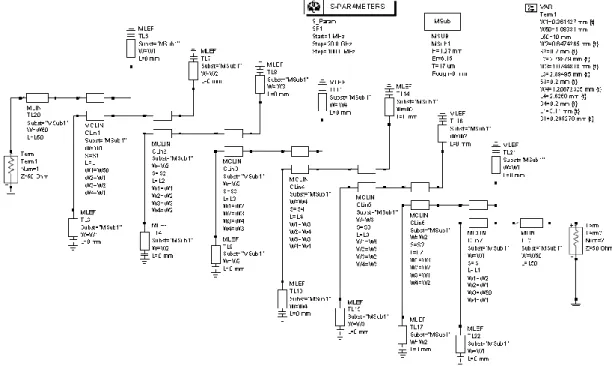
7.2. Network Microstrip components ... 93
7.3. Chapter summary ... 99
8. Conclusions and further work ... 101
8.1. Conclusions ... 101
8.2. Further work ... 102
9. References ... 105
xv
List of figures
Figure 1.1 - Radio over Fiber (RoF) network architecture ... 2
Figure 1.2 - RoFnet BS architecture ... 3
Figure 2.1 – Unshielded transmission line ... 9
Figure 2.2 - Microstrip line details ... 10
Figure 2.3 - Transmission line with load termination ... 15
Figure 2.4 - Short circuited transmission line ... 16
Figure 2.5 - Impedance behavior along a short circuit transmission line ... 17
Figure 2.6 - Open-circuited transmission line ... 17
Figure 2.7 - Impedance behavior along an open circuit transmission line ... 17
Figure 2.8 - Representation of capacitance and inductance of microstrip lines [12] ... 18
Figure 2.9 - Inductive and capacitive reactance example in microstrip line [12] ... 18
Figure 2.10 - Inductive and capacitive reactance example in microstrip line [12] ... 19
Figure 2.11 - Open-ended discontinuity ... 19
Figure 2.12 - Gap discontinuity ... 19
Figure 2.13 - Change in width discontinuity ... 20
Figure 2.14 - Bend effect ... 20
Figure 2.15 - Mitering the bend ... 20
Figure 2.16 - N-port microwave network ... 21
Figure 2.17 - ABCD system ... 23
Figure 2.18 - Cascade network example ... 23
Figure 2.19 - Richard Transformations ... 25
Figure 2.20 - Frequency response of raised-cosine filter. ... 28
Figure 2.21 - Impulse response of raised-cosine filter. ... 29
Figure 3.1 - Lowpass microstrip filter using stepped-impedance method ... 32
Figure 3.2 - T-equivalent circuit for a short length transmission line ... 33
Figure 3.3 - High characteristic impedance circuit equivalent ... 33
Figure 3.4 - Low characteristic impedance circuit equivalent... 33
Figure 3.5 - Lowpass filter prototype ... 35
Figure 3.6 - LPP for amplitude response calculation ... 35
Figure 3.7 - Stepped impedance method ... 37
xvi
Figure 3.9 - Corresponding bandpass filter response regarding the Butterworth lowpass filter
response ... 39
Figure 33 - Bandpass cascade with 3 coupled line sections equivalent [8] ... 40
Figure 3.11 - Couple resonator bandpass filters ... 41
Figure 3.12 - Power divider ... 42
Figure 3.13 - Power divider ... 42
Figure 3.14 - 2-way Wilkinson power divider ... 43
Figure 3.15 - S-parameters analysis of the Wilkinson power divider ... 44
Figure 3.16 - Multistage Wilkinson power divider ... 44
Figure 4.1 - Linecalc example ... 47
Figure 5.1 - First architecture proposal ... 49
Figure 5.2 - Architecture adopted ... 50
Figure 5.3 - Attenuation Vs normalized frequency for maximally flat filter prototypes [3] ... 51
Figure 5.4 - Prototype circuit for the lowpass filter ... 52
Figure 5.5 - Circuit schematic of the third order lowpass filter ... 53
Figure 5.6 - Frequency response of the third order lowpass filter ... 53
Figure 5.7 - Microstrip lowpass filter components ... 56
Figure 5.8 - Circuit Vs Microstrip implementation ... 57
Figure 5.9 - Schematic of the SRRCOS lowpass filter ... 58
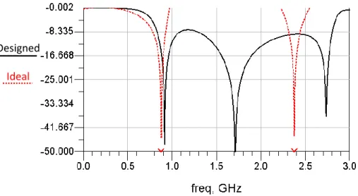
Figure 5.10 - Ideal SRRCOS lowpass filter response Vs Implemented version response... 58
Figure 5.11 – BS downlink bandpass filters ... 59
Figure 5.12 - Schematic of 12 GHz bandpass filter ... 62
Figure 5.13 - Layout of the bandpass filter with fc=12GHz ... 63
Figure 5.14 - S-parameters of the analytical Wilkinson power divider for 10 GHz ... 67
Figure 5.15 - S-parameters of the analytical Wilkinson power divider for 12 GHz ... 68
Figure 5.16 - Schematic of the multistage Wilkinson power divider ... 68
Figure 5.17 - S-parameters analysis of the multistage Wilkinson power divider ... 69
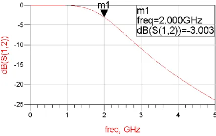
Figure 6.1 - Microstrip SRRCOS lowpass filter Layout ... 71
Figure 6.2 - Momentum dB(S(1,2)) results for the SRRCOS lowpass filter ... 72
Figure 6.3 - Momentum db(S(1,1)) and db(S(2,2)) results for the SRRCOS lowpass filter ... 72
Figure 6.4 - Momentum dB(S(1,2)) phase results for the SRRCOS lowpass filter ... 73
Figure 6.5 - Ideal schematic of the SRRCOS filter ... 73
Figure 6.6 - Eye diagram of the ideal raised cosine filter ... 74
xvii
Figure 6.8 - Eye diagram of the designed raised cosine filter ... 74
Figure 6.9 - Momentum eye diagram of the shaped pulses. ... 75
Figure 6.10 - S(1,2) dB of 12 GHz bandpass filter (Schematic Vs Momentum) ... 76
Figure 6.11 - Port matching and Insertion loss analysis (12 GHz centered filter) ... 76
Figure 6.12 - 12 GHz centered frequency bandpass filter Layout ... 77
Figure 6.13 - S(1,2) dB of 16 GHz bandpass filter (Schematic Vs Momentum) ... 77
Figure 6.14 - Port matching and Insertion loss analysis (16 GHz centered filter) ... 78
Figure 6.15 - Layout of the bandpass filter with fc=16 GHz ... 78
Figure 6.16 - S(1,2) dB of 9 GHz bandpass filter (Schematic Vs Momentum) ... 79
Figure 6.17 - Port matching and Insertion loss analysis (9 GHz centered filter) ... 79
Figure 6.18 - Layout of the bandpass filter with fc=9 GHz ... 80
Figure 6.19 – 11 GHz centred bandpass filter (Schematic Vs Momentum) ... 80
Figure 6.20 - Port matching and Insertion loss analysis (11 GHz centered filter) ... 81
Figure 6.21 - Layout of the bandpass filter with fc=11 GHz ... 81
Figure 6.22 - S(1,2) dB of 13 GHz bandpass filter (Schematic Vs Momentum) ... 82
Figure 6.23 - Port matching and Insertion loss analysis (13 GHz centered filter) ... 82
Figure 6.24 - Layout of the bandpass filter with fc=13 GHz ... 83
Figure 6.25 - S(1,2) dB of 15 GHz bandpass filter (Schematic Vs Momentum) ... 83
Figure 6.26 - Port matching and Insertion loss analysis (15 GHz centered filter) ... 84
Figure 6.27 - Layout of the bandpass filter with fc=15 GHz ... 84
Figure 6.28 - S(1,2) dB of 17 GHz bandpass filter (Schematic Vs Momentum) ... 85
Figure 6.29 - Port matching and Insertion loss analysis (17 GHz centered filter) ... 85
Figure 6.30 - Layout of the bandpass filter with fc=17 GHz ... 86
Figure 6.31 - Co-simulation of 10 GHz power divider ... 86
Figure 6.32 - S-parameters of the designed Wilkinson power divider for 10 GHz ... 87
Figure 6.33 - Layout of the multistage Wilkinson power divider ... 87
Figure 6.34 - Momentum S-parameters results without resistors ... 88
Figure 6.35 - Power divider with thin film resistor ... 88
Figure 6.36 - Momentum simulation results of the power divider with a 10 KΩ thin film resistor ... 89
Figure 6.37 - Testing schematic of the designed power divider ... 89
Figure 6.38 - Power divider outputs ... 90
Figure 6.39 - Power divider phase analysis ... 90
xviii
Figure 7.2 - Frequency shifting description ... 94 Figure 7.3 - SRRCOS filter shaped data ... 94 Figure 7.4 - Spectrum of all downlink channel frequencies ... 95 Figure 7.5 - Combined bandpass filter with 12 GHz centred frequency and power divider ... 95 Figure 7.6 - Combined structure (16 GHz) output ... 96 Figure 7.7 – Combined bandpass filter with 16 GHz centred frequency and power divider ... 96 Figure 7.8 - Combined structure (12 GHz) output ... 97 Figure 7.9 – 11 and 13 GHz centered signals spectrums ... 97 Figure 7.10 – 15 and 17 GHz centered signals spectrums ... 97 Figure 7.11 - Eye diagrams of the received signals ... 98
xix
Abbreviations
ADS Advanced Design System BS Base Station
CO Central Office EM Electromagnetic IL Insertion Loss
ISI Inter-Symbol Interference LTE Long Term Evolution
MMIC Monolithic Microwave Integrated Circuit NRZ Non Return to Zero
PCB Printed Circuit Board PDA Personal Digital Assistance RF Radio Frequency
RL Return Loss
RoFnet Reconfigurable Radio over Fiber network RSOA Reflective Semiconductor Optical Amplifier SCM Subcarrier Multiplexing
TEM Transverse Electromagnetic TM Transverse Magnetic TE Transverse Electric
VSWR Voltage Standing Wave Ratio WDM Wavelength Division Multiplexing WLAN Wireless Local Area Network Wifii Wireless fidelity
1
1. Introduction
1.1. Introduction
Currently wireless and mobile communications are witnessing a great development. In most developed countries, mobile phone penetration exceeds that of fixed phones. Wireless communications are entering a new phase where the focus is shifting from voice to multimedia services. Present mobile network users want to be able to use their mobile terminals and enjoy the same user experience as they do while connected at their fixed network at work or at home. WLAN hot-spots based on IEEE802.11 are a reality, and many consumer devices (Laptop PCs, mobile telephones, PDAs, etc) have Bluetooth so they can establish a Wireless Personal Area Network (WPAN). Due to the need of integrated broadband services (voice, data and video) wireless networks will need higher data transmission capacities well beyond the present day standards of wireless systems. Nowadays the main technologies vary from IEEE802.11 a/b/g (54Mbps) at 2.4 GHz and 5 GHz (Wi-Fi) until Wimax 802.16 (72 Mbps) between 2 and 66 GHz. Currently international standard bodies such as IEEE 802.15.3c working group are working on the standard for 60 GHz WPAN transmission systems. WPAN networks cover relatively short distances (10-30 meters) and can support high data rate applications (480 Mbit/s – 3 Gbit/s).
The limited propagation characteristics of mm-wave operating in the 60 GHz region lead to small cell sizes, therefore a large number of cells, served by base stations (BSs), are necessary to cover an operational area. This requirement has led to the development of system architectures where functions such as signal/routing/processing, handover and frequency allocation are carried out at the central office (CO). The best solution for connecting the CO with BSs in such radio network is via an optical fiber network, now known as radio over fiber (RoF) network [1]. By exploiting high bandwidth wavelength division multiplexing (WDM) networks, an integrated efficient fiber radio backbone network can be realized, where mm-wave carriers are modulated with data, placed on a particular mm-wavelength channel and delivered to a specific BS (Figure 1.1).
The multiple BSs providing wireless connectivity to users via mm-wave radio links are connected with a central office (CO) via an optical fiber access network, i.e. employing Radio over Fiber (RoF) technology.
2
Figure 1.1 - Radio over Fiber (RoF) network architecture
1.2. RoFnet Project
The RoFnet-Reconfigurable Radio over Fiber network is a project supported by the Portuguese Foundation for Science and Technology. This project proposes an innovative radio over fiber optical access network architecture, which combines a low cost Base Station (BS) design, incorporating reflective semiconductor optical amplifiers, with fiber dispersion mitigation provided by optical single sideband modulation techniques. Optical wavelength division multiplexing (WDM) techniques are used to simplify the access network architecture allowing for different Base Stations to be fed by a common fiber. Different wavelength channels can be allocated to different BSs depending on user requirements. Additionally, in order to improve radio coverage within a cell, it is considered a sectorized antenna interface. The combination of subcarrier multiplexing (SCM) with WDM, further simplifies the network architecture, by using a specific wavelength channel to feed an individual BS and four different subcarriers to drive the individual antenna sectors within the BS.
1.3. Downlink operation
A BS receives the downlink RF signal on a specific wavelength channel. The downlink signal is composed by 4 multiplexed subcarrier channels (11 GHz, 13 GHz, 15 GHz and 17 GHz) combined with an un-modulated RF (9 GHz) carrier as shown in Figure 1.2. The un-modulated RF carrier and the downlink signals are generated at the CO. At the BS, the
Central Office 1 2 3... N
3 downlink optical signal is split. One part is directed to the RSOA (Reflective Semiconductor Optical Amplifier), and the other part is detected by a high bandwidth receiver and delivered to the antennas. The four SCM channels are delivered to the four antenna sectors after being photo detected, split by a splitter designed in this dissertation and filtered by bandpass filters designed in this dissertation. The un-modulated RF carrier is filtered and used in the uplink operation.
1.4. Uplink Operation
The downlink optical carrier travels through the RSOA, where it is amplified and modulated by the uplink data channels, which has been combined and down converted to an Intermediate Frequency (IF). The un-modulated RF carrier act as local oscillators (LO) and is
i High Bandwidth Receiver Optical Circulator 1, 2, 3, 4 Optical Filter Downlink 2 Downlink 4 Downlink 3 Downlink 1 Uplink 3 Uplink 2 Electrical Bandpass Filters Splitter RSOA
To/From the Network
Carrier Uplink 4 Uplink 1 11 GHz 13 GHz 15 GHz 17 GHz 9 GHz
4
used to down-convert the uplink data to an Intermediate Frequency (IF), within the electrical bandwidth of the RSOA (1.2 GHz). The RSOA is directly modulated by the SCM uplink down-converted signals.
Using this technique, the uplink optical signal is generated by recovering a portion of the optical carrier used in the downlink transmission.
1.5. Dissertation Goals
The goal of this dissertation is to design, implement and test several lowpass and bandpass filters and one power divider that will be used in the RoFnet demonstrator. The work plan involves:
Installation and familiarization with EEsof Advanced Design System (ADS);
Bandpass and lowpass filters design;
Filters optimization;
Microstrip implementation and optimization;
Performance analysis using simulation methods.
1.6. Dissertation Organization
Following this short introductory section, chapter 2 discusses the theoretical fundaments needed for the work reported in this dissertation such as: transmission lines, scattering matrix, ABDC parameters, Richard’s transformation, Kuroda’s identities and digital transmission over bandlimited channels.
Chapter 3 describes the design procedure off both the lowpass and the bandpass filters required for this dissertation. Both filters design start from the choice of the appropriate lumped-element lowpass prototypes, followed by the transformation of these prototypes and the implementation in microstrip. An overview about power dividers is also given namely the Wilkinson power divider design approach.
The design environment (Advanced Design System) is described in chapter 4.
Chapter 5 reports to the design and implementation of the microstrip components. The BS filtering scheme is projected and the substrate is selected. The implementation of the lowpass filter, bandpass filters and power divider are also described in this chapter.
5 Momentum results are presented in chapter 6 as well as performance evaluation of the designed microstrip components.
After simulating each component separately, all the network components were brought together and simulated in chapter 7.
In chapter 8 conclusions regarding the accomplished work are presented as well as suggestions for future work.
7
2. Theoretical fundaments
2.1. Introduction
This chapter gives an overview of the theoretical background of microwave engineering used in this dissertation. The chapter starts with the basic definitions followed by a discussion of the propagations modes that exists in microstrip technology as well as discontinuities and stub tunes that may occur. Scattering matrix is also introduced as well as ABCD parameters, Richard’s transformation, Kurodas’s Identities and some construction methodologies regarding the projected filters and power splitters.
2.2. Microwave
Microwave means alternate current signals with a range of frequencies between 300 MHz and 300 GHz, corresponding to a wavelength () between c f 1m(300 MHz) and 1 mm(300 GHz). Most of the present research and wireless communications cover this frequencies range. When using these frequencies there are several aspects that have to be taken into account, i.e. radiation, coupling electromagnetic issues and frequency response of lumped (discrete entities that approximate the behavior of the distributed system under certain assumptions) circuit elements [2].
Standard circuit theory cannot solve the usual microwave problems for high frequencies (short wavelengths). Most of the times microwave components are distributed elements were phase and current change significantly with the physical dimensions of the device due to a dependence related to the microwave length. Thus, at low frequencies the wavelength is larger and there are not significant changes in the phase values across the component. On the other hand when dealing with high frequencies the wavelengths are much shorter than the dimensions of the component [3].
2.3. Transmission lines
Transmission lines are a very important factor in the design of integrated/high frequency circuits. Their length is expressed as a multiple or sub multiple of an electric or electromagnetic propagating signal wavelength and it can be expressed by degrees or radians.
8
Circuit theory and transmission line theory essentially differ in the electrical size. Circuit analysis assumes the physical dimension of a network much smaller then electrical wavelength. On the other hand, a transmission line may be a significant part of one or several wavelengths.
Important parameters that define a RF/microwave design are cost, electric performance, power and reliability. Costs can be reduced through the use a cheap technology, a cheap substrate, a set of simple components and a minimum number of interconnection.
Every printed transmission lines have their conductors impressed in a relatively small substrate. These lines can be uniform or non uniform, homogeneous or non homogeneous, lossy or lossless, protected or non protected, monolayer or multilayer and can be based in one or several substrates, i.e. different dielectrics. In uniform lines the characteristic impedance does not vary throw the line (opposite in the non uniform lines). In practice we can vary this impedance by changing the strip width.
When transmission lines have different dielectric (ex. microstrip lines), the transmission velocity depends on the transversal geometry of the line and the dielectric constants of the different mediums (ex. air and substrate material). Considering the dielectric constant of the line higher than the dielectric constant of the air and lower then the substrate material then the propagation of the electromagnetic waves is not realized as in a TEM (Transverse Electromagnetic) environment.
In a low loss transmission line the conductor thickness is 3 to 5 times higher than the human skin. Lossy transmission lines (conductor thickness smaller than the layer composation) can be used in the construction of terminals and atenuators.
When combining diferent transmission lines it is usefull to use multiple layers. With multiple layers it is possible to combine radio-frequencies and digital functions in an single module, i.e. the final circuit will be smaller, light, more reliable and will have more performance and lower costs [4].
Unshielded transmission lines are in direct contact with the air so they have to be protected from external radiation and electromagnetic interference (EMI) as Figure 2.1 illustrates.
9 This protection is provided by a shield around the transmission line [5].
2.3.1. Propagation
TEM (Transverse Electromagnetic waves) is the Stripline propagation mode. The conductor path is surrounded by similar dielectric materials, i.e. there are none electric or magnetic fields in the propagation direction. Thus, it has a phase velocity equal to the speed of light. One other common example beside Stripline that supports TEM propagation is the coaxial medium.
Microstrip lines propagation is characterized by a combination of TM (Transverse Magnetic) and TE (Transverse Electric). TM means that magnetic fields in the propagation direction do not exist, and TE means that there are not any electric fields in the propagation direction. Notice that the dielectric of the upper part of the microstrip line is air and the bottom is a PCB (Printed Circuit Board). In this case the TEM is not supported because the waves phase velocity of the air is different from the velocity in the PCB. However in a lower frequency (<=66 GHz) the magnetic and electric fields are sufficiently small in a way that these two propagation modes join themselves (quasi-TEM).
With low frequencies most of the electromagnetic field is distributed through the air, and with high frequencies the electromagnetic field travels in the PCB dielectric direction [4]. Therefore, a transmission line filled with a uniform dielectric can support a single and well-defined mode of propagation over a specified range of frequencies. This happens in TEM for coaxial lines, TE for waveguides, etc.
Figure 2.1 – Unshielded transmission line
Height Thickness Length
10
2.3.2. Microstrip transmission lines
A microstrip transmission line consists on a dielectric material sandwiched between metalized conductor(s) with a specific metallization circuit conductor on top and ground-plane on the back, as illustrated in Figure 2.2 .
This technology that can be easily integrated with other passive and microwave devices. The conductor with a specific Thickness (T) is printed on a thin grounded dielectric substrate with a specific height (h) and relative permittivityi (r).
Microstrip transmission lines characteristics include:
Good geometry that provides power handling, moderate radiation loss and
reasonable dispersion over a wide characteristic impedance range (about 15 to 150 Ohms) [7].
Easy incorporations of active devices, diodes and transistors;
Transmission of DC and AC signals;
Line wavelength is considerably reduced from its free-space value due to the substrate fields;
The structure can support moderately high voltages and power levels [6].
Concerning the design issues there are a few variables of high importance such as characteristic impedance and the propagation coefficient.
Therefore, a microstrip transmission line is a distributed parameter network where voltages and currents can vary in magnitude and phase along the line length.
The voltage (V) and current (I) on a transmission line along the z axis are given by: E – Electrical field H – Magnetic field Ground plane Dielectric Substrate Strip Conductor h T w
11
0 0 z z V z V e V e (2.1)
0 0 z z I z I e I e (2.2) The ze term describes wave propagation in the +z direction and the z e term represents the propagation in the –z. The complex propagation constant γ is given by
j R j L G j C
(2.3)
where represents the attenuation coefficient given by neper m. 1, the phase coefficient give byradians m. 1, R and L are the series resistance and inductance per unit length and G
and C are the shunt conductance and capacitance per unit length. The real part
causes signal amplitude to decrease along the transmission line and the imaginary part or phase constant determines the sinusoidal amplitude/phase of the signal along the transmission line at a constant time [9].These terms are not constants because they depend on the material, frequency or geometry in use.
Another important issue is the characteristic impedance. If we consider a travelling wave in the transmission line regardless its path (forward or backwards), the ratio of voltage to current is the characteristic impedance. Meaning that the impedance can be defined as:
0 R j L R j L Z G j C (2.4)
Assuming a lossless line with perfect conductors and dielectric material i.e. if no conducting currents exists between the two conductors and for that matter G=0 and R=0, then the propagation coefficient is:
j j LC
(2.5)
where at sufficiently high ratio frequencies the phase constant is given by equation (2.6).
LC
(2.6)
For a lossless transmission line (attenuation constant 0) the characteristic impedance can be written as:
12 0 L Z C (2.7)
A wider microstrip line occupies more area in the dielectric which results in larger capacitance per length. Considering C the capacitance of the transmission line with d dielectric filing and Cfreethe capacitance that has no dielectric filing we have the following relation:
d r free
C C (2.8)
However, the inductance per unit length is independent of the line’s dielectric and is given by: 2 1 free L c C (2.9)
In the above equation cis the propagation velocity of the electromagnetic wave in free space ( 3 10 m s8 ).
Equation (2.9) can be used in equation (2.7) to obtain equation (2.10).
0 1 r free L Z C c C (2.10)
The phase velocity for a TEM wave can be written as:
p r c v (2.11)
The wavelength of such propagation type is defined as:
0 r (2.12)
where 0is the free space wavelength. Therefore the wavelength is proportioned to the square root of the relative permittivity of the uniform dielectric material in which the line is implemented. So, for large permittivity materials the distributed components became shorter resulting in less occupied space [8].
13 Still, a microstrip line cannot support a pure TEM wave (phase velocity varies from the dielectric region (vp c
r ) to the air region (vp c), so the exact fields in a microstrip environment (quasi-TEM propagation mode) constitute a hybrid TM-TE wave, and for these matter approximations for the phase velocity, propagation constant and characteristic impedances will be obtained by the following quasi-static solutions[10]:p eff v c (2.13) 0 eff k (2.14) 0 0 0 k w
(2.15)In the above equations vpis the phase velocity and is the propagation constant. Phase velocity also depends on the effective dielectric constant (eff ) of the microstrip line which has a value between the air dielectric (1) and the region dielectric (r). It also depends on the conductor width (w) and the substrate thickness (h) as follows [3]:
1 1 1 2 2 1 12 r r eff h w (2.16)
Once the dielectric constant is known the characteristic impedance of the line can be calculated by equation (2.17).
0 60 8 ln para 1 4 120 para 1 1.393 0.667 ln 1.444 eff eff h w w w h h Z w h w h w h (2.17) The ratio wh based on specific characteristic impedance and dielectric constant takes the following form [3]:
14
2 8 for 2 2 1 2 0.61 1 ln 2 1 ln 1 0.39 for 2 2 A A r r r e w e h w w h B B B h (2.18) 0 1 1 0.23 0.11 60 2 1 r r r r Z A (2.19) 0 377 2 r B Z (2.20)Notice that with the previous equations it is also possible to calculate the width of the microstrip line. Substrate definition include the r and theh, by stipulating a characteristic impedance for the microstrip line will give access for the width calculation of the microstrip line.
Due to this propagation method the wavelength in a microstrip medium is given by:
0 g eff (2.21)
Considering two points in the same transmission line separated by one wavelength we can say that they have a phase difference of2 . With this it becomes possible to determine the wavelength along the transmission line:
( ) 2 0 2 2 2 wt z wt z (2.22)
Meanwhile, velocity of propagation (vp) can be expressed by the wavelength along the transmission line at the operation frequency:
p v f (2.23) p w v (2.24) Using equation (2.6):
15 1 p v LC (2.25)
The capacitance of a line that is uniformly filled with dielectric material is proportional tor. And the velocity in an air-filled transmission line is approximately the velocity of light in free space, so:
p r c v m s (2.26)
Where c is the free space velocity of light.
The total voltage and current of the line is a superposition of the incident and the reflected wave (standing waves). The voltage reflection coefficient is defined as the ratio of the amplitude of the reflected voltage by the amplitude of the incident voltage:
0 0 0 0 L L V Z Z V Z Z (2.27)
Figure 2.3 - Transmission line with load termination
When 0 there is no reflected wave. In order to achieve 0, the load impedance
L
Z must be equal toZ . In this case the load is matched to the line, since there is no reflection 0 of the incident wave.
When ZL Z0(mismatch), the line voltage magnitude is not constant and this voltage magnitude will oscillate along the line. The ratio of maximum voltage magnitude Vmaxto the minimum voltage magnitude Vminis defined as the voltage standing wave ratio (VSWR).
max min 1 1 V VSWR V (2.28) L Z 0 Z , IN ZIN
16
The input impedance of a lossless transmission line with length l 2, propagation constant and characteristic impedance Z , terminated by arbitrary load impedance 0 Z is L given as 0 0 0 tan tan L in L Z jZ l Z Z Z jZ l (2.29)
The electrical length (l) is normally given in degrees. If there is a short circuit in the line then ZL 0and from (2.29):
0tan
sc
Z jZ l (2.30)
When ZL (open circuit), using equation (2.26) the input impedance is:
0cot
oc
Z jZ l (2.31)
2.3.3. Lossless terminated lines (Short and Open circuit transmission lines)
How transmission lines are terminated is an important issue in practical designs. Consider a line terminated by a short circuit as follows:
One very important issue to consider regarding a transmission line is its impedance. And the impedance of a short circuit line has the following behavior:
l 0 L Z 0 0 Z l
17 For l 0 zin 0, however for l 4zin (open circuit). So, it is periodic in multiples of 2 [3]. For l 4the line becomes inductive, and for 4 l 2 it shows a capacitive response [11].
An open circuit terminated line is illustrated in Figure 2.6.
And the impedance behavior along an open circuit line is given by Figure 2.7. l 0 0 Z l L Z 0 in x z l 3 4 2 4
Figure 2.5 - Impedance behavior along a short circuit transmission line
Figure 2.6 - Open-circuited transmission line
0 in x z l 3 4 2 4
18
Notice that any multiple of 2 does not change the load impedance as seen above. However if the transmission line is a quarter wavelength length long, or l 4n 2 with
1, 2,3....
n it will transform/invert the load impedance [3].
For l 4 the line has a capacitive behavior, and for 4 l 2it shows an inductive response [11].
As seen, passive circuit elements can be represented by short-circuited or open-circuited lines. If an open-circuit is proposed, for different length values the correspondent circuits are illustrated in Figure 2.8.
If a short circuit line is used then length variation presents the following behaviours:
Thus, for different lengths values different behaviours will occur. This methodology is also used for line series resonant circuits as seen in Figure 2.10:
Figure 2.8 - Representation of capacitance and inductance of microstrip lines [12]
Figure 2.9 - Inductive and capacitive reactance example in microstrip line [12]
4 l l 4 4 l 2 l 2 l 4 l l 4 2 l 4 l 2 l
19
2.3.4. Discontinuities
Transmission lines present several types of discontinuities. Sometimes discontinuities results from mechanical or electrical transitions from one medium to another. Normally the effect of discontinuity is seen as an undesirable event, however sometimes discontinuities are deliberately implemented into the circuit in order to provide a certain electrical function. Either way, the discontinuities can be represented by an equivalent circuit. For this purpose usually the T or equivalent circuit is used [3].
Common microstrip discontinuities are the open ended that consist on a line over the substrate that which produces capacitor behaviour as illustrated in Figure 2.11.
The Gap discontinuity consists in two lines with open ended behaviours plus the additional coupling effect between them both as exemplified in Figure 2.12:
When different line sections have different width values then discontinuities effects appear in the circuit as well. Notice that common microstrip structures are based on this
Z0 ZZ0 0 Z0 CP Z0 Cg CP Z 0 Z 0
Figure 2.10 - Inductive and capacitive reactance example in microstrip line [12]
Figure 2.11 - Open-ended discontinuity
Figure 2.12 - Gap discontinuity
4 l
20
oscillating effect (example: lowpass filters). This event can be characterized with Figure 2.13 circuit [3].
Note: Other topologies can be consulted in [3].
Discontinuities at bends, step changes in widths and junctions cause degradations in circuit performance. These discontinuities introduce parasitic reactance that can lead to phase and amplitude errors, input or output mismatch and other undesirable effects. As seen, one approach is to include an additional circuit to adjust the circuit performance. However another approach can be taken. It consists on minimizing the effect of the discontinuities by slightly modifying the design structure. Consider Figure 2.14:
The right angle has a parasitic discontinuity capacitance caused by the increased conductor area near the bend. To eliminate this effect it is made a smooth bend with radius
3
r w or a slice of the corner must be taken off. This will reduce the excess capacitance of the bend (Figure 2.15). The optimums bend value depends on the characteristic impedance and the angle, so a miter length equal to 8 times the frequency used is a reasonable bend [3].
Z0 Z01
Z02
Z01 CP Z02
L L
Figure 2.13 - Change in width discontinuity
Figure 2.14 - Bend effect
Figure 2.15 - Mitering the bend
21
2.3.5. Stub tuning
Stub tuning is a matching technique that uses open-circuit or short-circuits length of transmission line connected at a curtained distance from the load. There are two important parameters to take into account with this methodology, i.e. the distance from the load and the value of reactance provided by the stub [3].
For practical consideration this method optimizes the circuit response and brings it back to zero.
2.4. Scattering Matrix
In microwave frequencies the idea of voltage, current and impedances is less descriptive when high networks are analysed. Instead, an analysis of incident and reflected waves is used.
The scattering matrix provides a good and complete description of a high frequency network as seen by its N ports, in terms of incident/reflected voltage travelling waves. For this matter this matrix becomes a valuable tool to evaluate per example the filters performance.
S-parameters can be measured by a network analyzer or calculated using network analysis techniques [3].
As seen in Figure 2.16 the Vn is the amplitude of the incident voltage wave on port n
and Vn is the amplitude of the reflected wave from portn. The scattering matrix
S is defined as: 2 , 2 V I 3 , 3 V I , N N V I 1 , 1 V I 2 , 2 V I 3 , 3 V I 1 , 1 V I , N N V I22 11 12 1 1 1 21 22 2 2 2 1 2 . N N N N NN N N S S S V V S S S V V S S S V V (2.32)
An element of the
S matrix is defined as:k ij 0 for k j i j V V S V (2.33)
Meaning that Sij (transmission coefficient) can be found by putting through port j an incident voltage wave of amplitude Vj and measuring the reflected wave amplitude Vi from port i. To avoid reflections all ports except port j should terminate in matched loads.
In the same manner S is the reflection coefficient seen through port i i i when all other ports are terminated in matched loads [3].
Consider a two port network. If we want to measure S11, we inject a signal at port one and measure its reflected signal. In practical experiments it is advised to only inject one signal at a time. If measuring S21, it is injected a signal at port 1, and then the resulting signal existing at port 2 is measured. For S12 a signal is injected into port 2, and measured in the leaving port 1, and for S22 it is injected a signal at port 2 and the reflected signal is measured at port 2 as well [13].
2.5. ABCD parameters
A large group of microwave networks consist of a cascade connection of two or more two-port networks. When this happens it is defined a 2x2 transmission or ABCD matrix for each two-port network.
The ABCD matrix is defined by:
1 2 2
V AV BI (2.34)
1 2 2
I CV DI (2.35)
23 1 2 1 2 V A B V I C D I (2.36)
These equations represent the following system:
Looking at the cascade network:
Which means that ABCD matrix of the cascade connection is equal to the product of the ABCD matrices representing individual ports.
3 1 1 1 2 2 1 1 1 2 2 3 V V A B A B I C D C D I (2.37)
This is a useful method when a more complicated microwave network that consists of cascades of this simpler two-ports need to be analyzed [3].
2.6. Richard’s Transformation
Richard’s transformation equals the behavior of lumped elements (L or C) and a given stub with respective characteristic impedance and length at precisely one frequency as illustrated in Figure 2.19.
The input impedance of short and open circuit transmission lines is given by equations (2.30) and (2.31).
However, transmission line stubs mathematically differs from the reactance of lumped inductors and capacitors as seen in equations:
I1 A B C D I2 V1 V2 Port 1 Port 2 I1 1 1 1 1 A B C D I2 V1 V2 2 2 2 2 A B C D I3 V3
Figure 2.17 - ABCD system
24 L Z jwL (2.38) C j Z wC (2.39)
Meaning that the impedances of transmission line stubs and lumped elements differ regarding its frequency, which leads to the following:
S IN L Z Z (2.40) O IN C Z Z (2.41) where S IN
Z is the input short circuit transmission line impedance and O IN
Z refers to the open circuit transmission line impedance. On the other hand if a single frequency is used than these functions will equalize and a transformation can be developed.
So, if a frequency (w ) satisfies the following equation: C
0 0 jw =jZ tan =jZ tan C C C P l w l v (2.42)
Or similarly in the lumped capacitor case:
0 0 =jZ cot w =-jZ cot C C C P j l C w l v (2.43)
Considering a stub transmission length of 8 and equation (2.22) the following wavelength is achieved: 2 P C C C v w (2.44)
Equation (2.30) will achieve the following expression:
0 0 0 jw =jZ tan = jZ tan Z 4 C Cl j (2.45)
25 Similarly, equation (2.31) acquires the referred expression:
0 0 =jZ cot = -jZ wC C j l C (2.46)
A short circuit stub with the same impedance as an inductor L at frequency wC can be achieved if the characteristic impedance of the stub is set tow L . Likewise an open circuit C
stub can be designed if his characteristic impedance has the value 1
C
w C.
Richard Transformations:
Richard’s Transformations do not result in perfect replacements for lumped elements i.e. the stubs do not behave like capacitors and inductors. What happens is that the transformation is perfect and impedances are equal at a certain frequencyw . ThisC w is also C known as the cutoff frequency of a lumped element filter design whose inductors and capacitances were replaced by Richard’s transformations [3].
2.7. Kurodas’s Identities
The four Kuroda identities use redundant transmission line sections to allow implementation of microwave filters. They separate transmission line stubs, transforms series stubs into shunt stubs and vice-versa and replaces characteristic impedances that are difficult to implement with more practical ones. The additional transmission line segments are called unit elements and are 8 long at the cutoff frequency and they are commensurate (all lengths of all the stubs are the same) with the stubs that realize the inductors and capacitors of the prototype design. The four identities within each specific box representing a unit element (transmission line) of the specified characteristic impedance and length 8 atc are
Short-Circuit Open-Circuit jBC jXL jXL L C jBC 8 at wC 8 at wC Z0=L Z 0=1 C
26
available in [3]. For every identity the equivalence between the two networks can be proved demonstrating that their ABCD matrices are equal [3].
2.8. Digital transmission
2.8.1. Digital transmission trough band limited channels
The transfer function of a transmission channel, H(f) may be expressed in the form of equation (2.47).
( ) j f
H f H f e (2.47)
where H f is the amplitude response and the phase response. A channel is ideal or non-
distorting if within the bandwidth W occupied by the transmitted signal, H f
is constant and
f is a linear function of the frequency. Real transmission channels, such as coaxial cables or optical fibers are band limited and non ideal. Therefore when a digital signal with infinite bandwidth, such as a sequence of rectangular pulses is transmitted through the channel it becomes distorted causing inter-symbol interference (ISI).2.8.2. Nyquist criteria for zero ISI
Typically, the transfer function of the channel and the transmitted pulse shape are specified, and the problem is to determine the transfer functions of the transmitter and receiver filters so as to obtain at the decision circuit zero ISI.
Let p(t) to be the pulse shape at the output of the receiving filter. In the absence of noise and assuming no transmission loss, the output waveform is given by equation (2.48).
k d kpt t KT a t y (2.48)ak represents the amplitude of the k pulse and p(t) is the shape of the elementary pulse, in
order to have ISI=0,
,... 2 , 0 0 1 T T t t t p (2.49)27
f f W P 0 (2.50) where, T T W 2 1 0 2 1 (2.51)The Nyquist vestigial-symmetry theorem states that equation (2.49) is satisfied if p(t) has the form of equation (2.52).
T t sinc t p t p (2.52) with,
0 0 1 p t P f f p P f df
(2.53)Infinitely many functions satisfy the Nysquist conditions, including the case when
t 1 p and
T t sinc tp . This pulse shape allows band limited signaling at the maximum rate r=2W. However, synchronization and practical implementation are an issue.
2.8.3. Raised Cosine shaping
Raised cosine shaping filters are used to minimize inter symbol interference (ISI) and to avoid the synchronization problem mentioned in the previous section. It eliminates ISI as its impulse response is zero at all nT (except n=0, and T the sampling interval). For this matter a good choice is to use a square root raised cosine filter (SRRCOS) at transmitter and receiver end of the communication system, so the final shape will be raised cosine [14].
The spectrum of the raised cosine filter shows odd symmetry about1 2T. The raised cosine frequency response can be written as [15]:
28
1 , 0 2 1 1 1 1 cos , 2 2 2 2 1 0, 2 T f T T T H f f f T T T f T (2.54)where
is the roll-off factor, which is the measure of the bandwidth occupied beyond the Nyquist bandwidth of 12T also called excess bandwidth. The roll-off factor is given by:
2 1 2 2 s f f T f R T (2.55)
Plus, f is the excess bandwidth and R the symbol rate given by: s 1
s
R T (2.56)
The bandwidth is given in expression (2.57).
1 1 2 s
W R (2.57)
The roll of factor varies from zero to one and along with this variation the frequency domain response takes the form of Figure 2.20.
-2 -1.5 -1 -0.5 0 0.5 1 1.5 2 0 2 4 6 8 10 12 14 frequency, f/W a m p lit u d e , |G (f )|
Frequency domain representation of raised cosine pulse shaping filters Alpha=0 Alpha=0.5 Alpha=1
29 The impulse response has its zeros in T, 2T, 3T and by varying the roll off factor the harmonics of the response become more or less flatten as it can be seen in Figure 2.21.
-10 -8 -6 -4 -2 0 2 4 6 8 10 -0.4 -0.2 0 0.2 0.4 0.6 0.8 1 time, t/T a m p lit u d e , g (t )
Time domain waveform of raised cosine pulse shaping filters Alpha=0 Alpha=0.5 Alpha=1
Figure 2.21 - Impulse response of raised-cosine filter.
When 1, the non-zero portion of the spectrum is a pure raised cosine:
1
1 1 cos , 2 H f fT f T (2.58)When approaches zero:
H f rect fT (2.59)
In the equation aboverect fT
refers to a rectangular function [15][17].2.9. Chapter Summary
Microwave transmission lines were explained, as well as their importance in the design of integrated/high frequency circuits. Short and open circuit transmission lines are studied and the respective impedance behavior regarding the length of these transmission lines are discussed.
Eventually, discontinuities results from mechanical or electrical transitions from one medium to another and is normally considered as an undesirable effect, however, in certain cases discontinuities are deliberately implemented into the circuit in order to provide a certain

![Table 1 - Element values for the maximally flat lowpass filter prototypes [3]](https://thumb-eu.123doks.com/thumbv2/123dok_br/18500079.901892/60.892.85.770.99.548/table-element-values-maximally-flat-lowpass-filter-prototypes.webp)
![Figure 5.3 - Attenuation Vs normalized frequency for maximally flat filter prototypes [3]](https://thumb-eu.123doks.com/thumbv2/123dok_br/18500079.901892/75.892.236.709.738.1087/figure-attenuation-normalized-frequency-maximally-flat-filter-prototypes.webp)