Abstract— This paper, a compact low-pass filter (LPF) with an Elliptic function response using P-shaped resonators is presented. The LPF with simple structure results in the low insertion loss less than 0.1 dB and high return loss better than 20 dB, in the pass-band. The proposed filter with a -3 dB cutoff frequency of 2.61 GHz is fabricated and measured. The measured results show that the proposed LPF has significant advantages such as a wide stop-band from 2.9 GHz to 17.3 GHz with the suppression level better than -20 dB, and it has an acceptable sharp frequency response in the transition band. The measurement results are in good agreement with the simulation results.
Keywords— Low Pass Filter (LPF), Microstrip, P Shaped, Stop-band
I. INTRODUCTION
Microwave low-pass filters are the important blocks in modern wireless communication systems to
eliminate unwanted signals [1]. Compact microstrip low-pass filters with wide stop-band, sharp roll
off, high suppression in the stop-band and low insertion loss are widely demanded in microwave
technologies. In [1], a LPF using radial stubs is presented, which provides an ultra wide stop-band;
however, has a very gradual transition band. A LPF with low insertion and wide stop-band using
modified semi-Elliptic and semi-circular microstrip patch resonator is presented in [2]. This filter has
a low return loss in the pass-band and a large circuit size. In [3], a low-pass filter using coupled-line
hairpin unit, semi-circle defected ground structures and semi-circle stepped-impedance shunt stubs is
fabricated that has a sharp roll off, but it has narrow stop-band with -20 dB rejection and low return
loss in the pass-band. Also, it does not have a small size. A quasi Elliptic low-pass filter using
symmetric rectangular coupled capacitors is presented in [4], which provides compact size and good
return loss in the pass-band. But the rejection region is narrow; in addition, the transition band is
gradual. In [5], a LPF using coupled-line hairpin units is presented. The filter does not have wide
Compact Microstrip Low
-
pass Filter with
Wide Stop
-
band Using P
-
Shaped Resonator
Mohsen Hayati, Masoom Validi
Department of Electrical Engineering, Kermanshah Branch, Islamic Azad University, Kermanshah, Iran Electrical Engineering Department, Faculty of Engineering, Razi University, Kermanshah-67149, Iran.
[email protected], [email protected]
Farzin Shama,
Young Researchers and Elite Club, Kermanshah Branch, Islamic Azad University, Kerma nshah, Iran. [email protected]
Milad Ekhteraei
In this paper, a compact microstrip low-pass filter with a wide stop-band using P-shaped resonators
is presented that result in low insertion loss and high return loss in the pass-band. The proposed filter
has simple shape and achieves good performance in the stop-band region, pass-band and transition
band.
II. FILTER DESIGN
The design process of the proposed filter is as follows:
i- Design of an Elliptic function resonator to achieve sharp cutoff response.
ii- Provide an LC model of the proposed P-shaped resonator in order to optimize the resonator.
iii- Design of the proposed filter that include the combination of the proposed resonator with
suppressing cells.
A. Design of Elliptic Function Resonator
A prototype Elliptic-function low-pass resonator with desired cutoff frequency is selected, and the
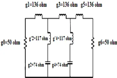
values of the circuit’s elements are calculated [6], as shown in Figure 1. The characteristic
impedances for microstrip lines with width 0.2 and 0.3 and 0.8 mm are 136 Ω and 117 Ω and 74 Ω,
respectively.
Fig. 1. The LC model of prototype Elliptic function low-pass resonator
To realize the Elliptic resonator, a P-shaped microstrip layout is proposed, as shown in Figure 2. In
this layout, to realize the Elliptic function LC circuit, the high impedance lines with width of W1 and
W2 are equivalent to inductance and the semicircle open-stubs are equivalent to capacitor. The
coupling capacitance, between the semicircle open-end stubs, is ignored in this realization because the
Fig. 2. The proposed resonator
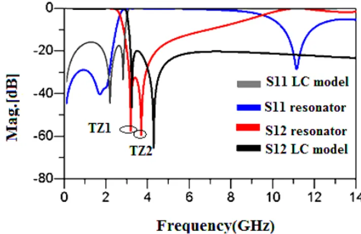
The S-parameters of the P-shaped resonator are compared with the LC equivalent circuit frequency
response, as shown in Figure 3. It can be seen clearly that the cutoff frequency of the proposed
resonator is adjusted to 2.6 GHz with an Elliptic response.
Fig. 3. The frequency response of the prototype filter
The resonator creates two transmission zeros at 3.3 GHz and 3.9 GHz with corresponding
attenuation levels of -55 dB and -54 dB, respectively, where return loss in the pass-band is 30 dB. By
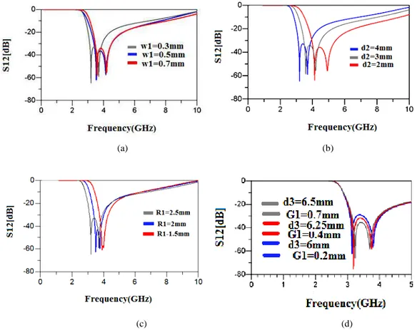
increasing the width of W1 from 0.3 mm to 0.7 mm as shown in Figure 4 (a), decreasing d2 from 4
mm to 2 mm as shown in Figure 4 (b) and decreasing R1 from 2.5 mm to 1.5 mm as shown in Figure
4 (c), the transmission zeros move away from the lower frequencies. Therefore, the location of the
transmission zeros can be controlled by tuning the values of W1, d2 and R1.
With the increment of d3 from 6mm to 6.5mm with a step of 0.25mm, the attenuation level in the
stop-band region is increased from 3.2GHz to 4 GHz. Also, the effect of increment of G1 is similar to
the effect of the increment of d3. The effect of variation of d3 and G1 on the frequency response of
the resonator is shown in Figure 4(d). But with increment of w2 from 0.2mm to 0.6mm with step of
0.2mm, the attenuation level in the stop-band region is decreased, as shown in Figure 4(e). Therefore,
the dimensions of these parameters are optimized using optimization tools in the ADS software,
(a) (b)
(c) (d)
Fig. 4. (a) The S12 parameter of the proposed resonator as a function of W1 (b) The S12 parameter of the proposed resonator
as a function of d2 (c) The S12 parameter of the
Proposed resonator as a function of R1 (d) The S12 parameter of the proposed resonator as a
function ofd3 and G1 (e) The S12 parameter of the proposed resonator as a function of W2
B. The LC model of the proposed P-shaped resonator
The accurate LC model of the proposed P-shaped resonator is shown in Figure 5. As observed, Cg1
is the coupling capacitance between the semicircle open-end stubs, L1 and L2 represent inductances
of the main transmission line between input and output ports, L3 represents inductance of the stubs,
Cr is the capacitance of the radial open-end stubs with respect to the ground.
L3
L1 L2
L1 L2
Cr Cr
Cg1
L1
L3 L3
L1 L3
Cr
Cg1 Cr
By considering the open-end radial stubs as a unit, which is shown in Figure 6; the capacitance of
the radial stub can be obtained through one port -parameter using (1) and (2) [7].
)) ( ( 2 1 in Z ima g f C (1)
where Zin can be calculated as:
] ) 1 ( ) 1 ( [ 50 11 11 S S Zin (2)
(a) (b) (c)
Fig. 6.The configuration of the capacitive elements. (a)Radial stub. (b)Straight stub. (c)The equivalent circuit of (a) and (b).
For the straight stub, the equivalent capacitance can be directly obtained as (3) when the effective electrical length is less than a quarter-wave length [7
]:
s s fZ L C 2 ) tan( (3)
where β, Ls and Zs represent the propagation constant, length of the straight stub and impedance of
the straight stub, respectively. The other parameters of the accurate LC model of the proposed
resonator are obtained from [6]:
c i i f g g Z L 2 0 0 (4) c i i f g Z g C 2 0 0 (5)
where, Li and Ci represent the inductance and capacitance of the transmission line, respectively, Z0
represent source impedance, fc is cutoff frequency and g0 and gi represent either the inductance of a
series inductor or the capacitance of a shunt capacitor.
Therefore, in the first step, the LC model of the elliptic function resonator with desired
characteristics is designed. The parameters of the LC model of the proposed resonator are obtained
from Equations (4) and (5). Then after obtaining LC values, in order to improve the accuracy of the
response, the LC values are optimized by tuning tool in the ADS software, which uses the local
gradient optimization process. The LC value of the proposed LPF is shown in Table.1.
The optimized dimensions of the proposed P-shaped layout are: d1= 10 mm, W1= 0.3 mm, d3 = 6.5
Elements L1(nH) L2(nH) L3(nH) Cr (pF)
Calculated
L-C values 0.82 5.9 3.43 0.17
Optimized
L-C values 0.82 5.11 3.23 0.13
The physical lengths of the high- and low-impedance lines may be found by [6]:
) ( sin
2 0
1
Li i c gLi
Li
Z L
l
(6)
) (
sin
2 0
1
ci i c gCi
Ci CZ
l
(7)
where, lLi and lci represent the dimension's inductance and capacitance of the transmission line, Z0
represent source impedance, ωc is cutoff frequency, λgL and λgc represent guided wavelengths (mm)
for inductance and capacitance, respectively.
C. Design of the Proposed Filter
To reach wide stop-band with good suppression of the harmonics in the stop-band region, a
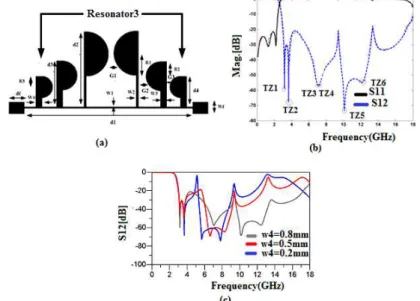
multiple resonator with different dimensions is used. In first step, two P-shaped units are added to the
proposed resonator, as shown in Figure 7 (a). Figure 7(b) shows that the resonator 2 creates TZ3 and
TZ4 in the stop-band region. On the other hand the stop bandwidth with -17dB attenuation level up to
9 GHz is created.
Fig. 7. (a) The proposed cascaded P-shaped resonator. (b) The simulated s-parameters of proposed cascaded P-shaped
resonator. (c) The S12 parameter of the proposed resonator as a function of d3 (d) The S12 parameter of the proposed
As shown in Figure 7(c), by increasing d3 from 6mm to 10mm, the transmission zeros are moved to
the lower frequency (with considering the proposed LC model in Figure 5, by increasing d3, the
capacitance of Cr and inductance of L3 are increased) . When w3 is decreased from 0.8mm to 0.2mm
as shown in Figure 7(d), the transmission zeroes are moved to the lower frequency (with considering
the proposed LC model in Figure 5, by decreasing w3, the inductance of L3 is increased). The
proposed structure does not have wide stop-band. To obtain a LPF with better stop bandwidth and
attenuation level, third resonator is added to the structure of Figure 7(a). Each of P-shaped units adds
a transmission zero, at about 11 GHz that can guarantee the harmonics rejection in higher frequencies
than 9 GHz, as shown in Figure 8. The layout of the proposed LPF consists of six P-shaped units, as
illustrated in Figure 9 (a). Although the new added P-shaped units improve the stop-band region
characteristics significantly, but it can create a more insertion loss in the pass-band imperceptibly. The
structure parameters of the filter are: Wf = 1.5 mm, df = 2 mm, W1 = 0.2 mm, d1= 22 mm, W2 = 0.3
mm, d2 = 10 mm, W3 = W4 =0.8 mm, d3 = 6 mm, d4 = 4 mm, R1 = 2.5 mm, R2 = 1.5 mm, R3 = 1
mm, G1 = 0.7 mm, G2 = 1 mm, G3= 0.4 mm.
Fig. 8. The effect of adding a new P-shaped unit to the proposed cascaded P-shaped resonator.
moved to the lower frequency. Therefore, the location of transmission zeros in the stop-band can be
easily controlled by the variation of dimensions of the proposed filter parameters.
III. MEASUREMENTSANDRESULTS
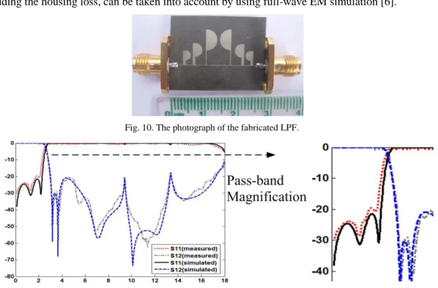
The proposed LPF has been fabricated on a RT/Duroid 5880 substrate with a relative dielectric
constant εr = 2.2, thickness h = 20 mil and loss tangent of 0.0009. The photograph of the fabricated
filter is shown in Figure 10. The Simulations and measurements are performed using ADS software
and HP 8757A network analyzer, respectively. The simulated and measured results are shown in
Figure 11. A metallic cover is normally required for most microstrip circuit applications, such as
filters. The presence of conducting top and side walls will affect both the characteristic impedance
and the effective dielectric constant. In practice, a rule of thumb may be applied in the filter design to
reduce the effect of cover: the height up to the cover should be more than 8 times and the distance to
walls more than 5 times the substrate thickness. For more accurate design, the effect of cover,
including the housing loss, can be taken into account by using full-wave EM simulation [6].
Fig. 10. The photograph of the fabricated LPF.
Fig. 11. The measured and simulated S-parameters of the fabricated LPF.
The filter has a -3 dB cutoff frequency equal to 2.61 GHz and insertion loss less than 0.1dB in the
pass-band from DC to 2 GHz. The return loss is better than 21 dB in the pass-band. The insertion loss
has the suppression level better than -20 dB from 2.9 up to 17.3 GHz that obtains a wide stop-band.
The return loss in the stop-band region is very close to 0 dB. The size of the LPF is only 22×10 mm2.
Table 2 summarizes the performance of some other works. In this Table:
off, which is defined as below [8]:
C
S f
f
max min
(8)
where αmax is the -20 dB attenuation point; αmin is the -3 dB attenuation point; fs is the -20 dB
stop-band frequency; and fc is the -3 dB cutoff frequency. The Relative stop-band bandwidth (RSB) is
given by [8-9], where a higher RSB represents a wider stop-band region:
fr equency center
stopba nd
dB stopba nd
RSB (20 ) (9)
The suppression factor (SF) is based on the stop-band suppression. A higher suppression degree in
the stop-band leads to a greater SF. For instance, if the stop-band bandwidth is calculated under -20
dB restriction, then the SF is considered as 2. The normalized circuit size (NCS) is given by [8],
which a lower NCS represents a smaller circuit size:
2 ) ( g width lenght size physica l NCS (10)
This is applied to measure the degree of miniaturization of diverse filters, where λg is the guided
wavelength at -3 dB cutoff frequency. The architecture factor (AF) can be recognized as the circuit
complexity factor, which is signed as 1 when the design is 2D and as 2 when the design is 3D. Finally,
the figure of merit (FOM) is defined as below [8] and with the above discussion a higher FOM
represents a better high-performance LPF:
AF NCS SF RSB FOM
(11)
TABLE II.PERFORMANCE COMPARISON WITH OTHER WORKS.
Ref. ζ RSB NCS SF FOM
[1] 5.28 1.66 0.01 2 1159
[2] 30.35 1.42 0.061 2 1413
[3] 28.33 1.42 0.025 1 804
[4] 37.8 1.16 0.02458 2 3576
[5] 34 1.15 0.02072 1.7 3774
[9] 29.3 1.49 0.1456 2 600
[10] 52.85 1.22 0.0288 2 4478
[11] 84 0.67 0.0857 2 985
[12] 70 1.40 0.0272 1 1200
[13] 16.9 1.38 0.0095 1.5 3682
This work 47.22 1.48 0.020 2 6988
IV. CONCLUSION
A compact microstrip low-pass filter using P-shaped resonators is proposed. This filter has a simple
structure for easy fabrication. The proposed filter is simulated, fabricated and measured. Good
agreement between measurement and simulation results is observed in both the pass-band and
stop-band regions. The measured results show that the proposed LPF has many satisfactory features such
as compact size, low insertion loss, sharp roll off and wide stop-band in comparison with other works.
The LPF with described performance can resolve the requirements in wireless communication
systems and microwave applications.
REFERENCES
[1] Ma, K., Yeo, K.S. and Leoe, W.M.: Ultra-wide rejection band lowpass cell, Electronics Letters. 48, 99 –100 (2012).
[2] Hayati, M., Sheikhi, A. and Lotfi, A.: Compact lowpass filter with wide stopband using modified semi-elliptic and semi-circular microstrip patch resonator. Electronics letters. 46, 1507-1509 (2010).
[3] Wei, F., Chen, L., Shi, X.W., Huang, Q.L. and Wang, X.H.: Compact lowpass filter with wide stop-band using coupled-line hairpin
unit. Electronics letters. 46, 88-90 (2010).
[4] Li, L. and Li, Z.F.: Compact quasi-elliptic lowpass filter using symmetric rectangular coupled capacitors. Electronics letters. 44,
124-125 (2008)
[5] Sha, L., Lei, Z. and Sheng, S.: Stopband-Expanded Low-Pass Filters Using Microstrip Coupled-Line Hairpin Units. IEEE Microwave
and wireless components letters. 18, 506-508 (2008).
[6] Hong, J.S. and Lancaster, M.J.: Microstrip Filters for RF/Microwave Applications, New York John Wiley & Sons, Inc (2001).
[7] Ma, K. and Yeo, K., S.: New Ultra-Wide Stopband Low-Pass Filter Using Transformed Radial Stubs. IEEE transaction on microwave
theory and techniques. 59, 604-611 (2011)
[8] Wang, J.P., Ge, L., Guo, Y. X. and Wu, W.: Miniaturized microstrip lowpass filter with broad stopband and sharp roll off. Electronics
letters, 46, 573-575 (2010).
[9] Hayati, M. and Shama, F.: Compact Microstrip Low-Pass Filter with wide stopband using symmetrical U-shaped resonator. IEICE
Electronics Express 9.3, 127-132 (2012).
[10] Hayati, M., & Yousefzadeh, Y.: Compact Lowpass Filter with Wide Stopband Using Windmill-Shaped Resonator. Arabian Journal for
Science and Engineering, 39(4), 3033-3038 (2014)
[11] Raphika, P. M., P. Abdulla, and P. M. Jasmine. : Compact lowpass filter with a sharp roll-off using patch resonators. Microwave and
Optical Technology Letters 56.11, 2534-2536 (2014).
[12] Faraghi, Ahmad, Mohammad Ojaroudi, and Noradin Ghadimi. : Compact microstrip low-pass filter with sharp selection characteristics
using triple novel defected structures for UWB applications. Microwave and Optical Technology Letters 56.4, 1007-1010 (2014).
[13] Chen, Xianhong, et al.: Compact lowpass filter with wide stopband bandwidth. Microwave and Optical Technology Letters 57.2,