Available online at
http://www.iaeme.com/ijeet/issues.asp?JType=IJEET&VType=7&IType=3 ISSN Print: 0976-6545 and ISSN Online: 0976-6553
Journal Impact Factor (2016): 8.1891 (Calculated by GISI) www.jifactor.com © IAEME Publication
DESIGN OF A MULTIFUNCTIONAL
FLYBACK DC-DC CONVERTER WITH
CURRENT CONTROL
Fernando Santos
Polytechnic Institute of Viseu, School of Technology and Management of Lamego, Portugal
Humberto Jorge
Department of Electrical and Computer Engineering, University of Coimbra, INESC Coimbra, Portugal
Sérgio Cruz
Instituto de Telecomunicações and Department of Electrical and Computer Engineering, University of Coimbra, Portugal
ABSTRACT
This paper proposes a set of design techniques to build a DC-DC converter for the interconnection of different sources of renewable energy with storage elements and flexible load profiles. This type of multifunctional DC-DC converter is essential to provide the dispatch of energy generation to storage connected to the DC bus or allow energy exchange with the AC network, with different decision modes as a function of the state of charge of batteries, with the forecast of the consumption of a house with renewable production. This work emphasizes the application of a method to design switched mode flyback converters with current control capabilities on the output side. The paper discusses in detail the design of the different parts of the converter: the power circuit, the control signals and the auxiliary power supply. The experimental results obtained with the prototype of the DC-DC converter built validate the theoretical analysis and the proposed design techniques. Moreover, the results demonstrate the good dynamic performance of the converter, which exhibits a good current control capability on the output side, being able to follow closely the reference value in a very short period of time, and ensuring at the same time a stable steady-state response.
Key words: DC–DC Converters, Flyback Topology, Current Control,
Cite this Article: Fernando Santos, Humberto Jorge and Sérgio Cruz, Design
of A Multifunctional Flyback Dc–Dc Converter with Current Control.
International Journal of Electrical Engineering & Technology, 7(3), 2016, pp.
57–72.
http://www.iaeme.com/ijeet/issues.asp?JType=IJEET&VType=7&IType=3
1. INTRODUCTION
The two main methods to reduce consumer energy costs in a house are improving energy efficiency and increasing the use of renewable energy sources. In the last case, there is a problem related to the fact that most of the energy produced by these sources do not match the home energy consumption. The solution to this problem may reside in the use of energy storage devices in order to adjust the energy generation to the consumption demand.
On the other hand, to promote efficiency in distribution networks, it is convenient to locate the energy storage devices closer to the consumer loads, thus reducing losses in the distribution of electricity as well as increasing the voltage stability [1].
Another positive aspect of locating the energy storage near the loads is to give consumers the ability to be energy suppliers as well, making them an active element of the investment needed to shift from a carbon-based to a renewable energy-based economy. In this context, there is a need to develop energy storage modules for low voltage end-users. These modules can then be integrated and linked with generation modules of different technologies and different manufacturers [2].
The work reported in this paper is part of a broader work, whose main goal is to develop a multifunctional DC/AC power supply system for a home with renewable energy generation, in the context of a liberalized energy market. Fig. 1 shows the power system built with the multifunctional DC/AC system. The different renewable energy sources, as well as the energy storage devices - batteries and supercapacitors - are interconnected through different DC-DC converters. The DC bus supplies a DC load and is interconnected to the grid through an inverter and an autotransformer for adapting the voltage level. This allows the bidirectional exchange of energy between the DC bus and the AC network. The inverter is responsible for the regulation of the voltage in the 24 V DC bus. This voltage value was selected because it eases the association of storage and production devices and is sufficient to supply the load without leading to excessive current values.
AC load AC network (230V/400V, 50 Hz) Inverter SEMIKRON 132GD120-3DUL DC load DC-DC converter Batteries Supercapacitors Renewable source I 24V 27V Ib1 Ib2 ISC1 ISC2 IE IPV1 ICDC 24V ICAC Autotransformer Renewable source II DC-DC converter converterDC-DC DC-DC converter DC-DC converter DC-DC converter
Figure 1 Developed multifunctional DC/AC power supply system.
A dispatch algorithm, in conjunction with the controlled DC-DC converters, regulates the current value that each storage element or renewable source supplies to the DC bus.
2. COMMON DC-DC CONVERTER TOPOLOGIES
Different topologies can be used in DC-DC converters, which generally are grouped into two main categories: non-isolated and isolated converters.
Table I shows a comparison of the most common types of DC-DC converters [3-6].
TABLE I Common Types of DC-DC Converters
Topology Isolated Cost Magnetic Components Universal input?
Vout < Vin range
Vout > Vin range
Buck No 1 Inductor No Yes No
Boost No 1 Inductor No No Yes
Buck –Boost No 1 Inductor No Yes Yes
Sepic No 1.2 Two Inductors No Yes Yes
Cuk No 1.2 Two Inductors No Yes Yes
Flyback Yes 1.5 Transformer Yes Yes Yes
Forward Yes 1.8 Transformer and Inductor Yes Yes Yes
Push-Pull Yes 1.8 Transformer and Inductor No Yes Yes Half Bridge Yes 2 Transformer and Inductor Yes Yes Yes
Resonant LLC Yes 2 Transformer Yes Yes Yes
Among the configurations mentioned in Table I, the flyback and the resonant LLC converters are the isolated converters with the smallest number of magnetic components [3]. In addition, the flyback converter is the one that presents less electronic components [7].
Flyback converters have been an attractive solution in various power conversion applications due to their topological advantages such as simple structure, low cost, and galvanic isolation between the input and output sides [8, 9].
Given these advantages, the flyback converter was the adopted topology for all DC-DC converters shown in Fig. 1.
3. OPERATING PRINCIPLE OF FLYBACK CONVERTERS
A. Topology
Fig. 2 shows the topology of a flyback converter [10]. Initially, the power switch is closed to allow the circulation of current in the primary circuit of the transformer, being the energy stored in its magnetic circuit. Next, the power switch is opened and the energy stored in the core is transferred to the secondary circuit of the transformer, feeding the load [11].
VOUT Load VIN + -+ IIN IOUT T1 Driver circuit C1 -D1 MOS1
Figure 2 Topology of a flyback converter
B. Operation mode
There are two distinct operation modes for flyback converters: the continuous mode and the discontinuous mode [10], [12]. Fig. 3 shows the typical waveforms for these two operation modes.
The discontinuous mode happens when all energy stored in the transformer during an energy storage period (“on” period) is transferred to the output during the flyback period (“off” period) while in a continuous mode, part of the energy stored in the transformer during the “on” period remains in the transformer at the beginning of the next switching period [5], [12], [13].
Figure 3 Current waveforms for the two operation modes of a flyback converter.
As can be seen in Fig. 3, in the continuous mode the current in the primary side of the transformer has a higher initial value. This higher current leads to higher switching losses in the converter, and requires s transformer with a higher inductance, thus increasing its size and cost [14], [15].
Hence, the DC-DC converter designed in this paper is to be operated in a discontinuous mode, in order to have lower losses in transformer and a higher converter efficiency, but still being able to maintain a high voltage level at the output side.
4. PROPOSED CONVERTER
A. Design
The Flyback transformer used in the converter is the ETD49 type for high frequencies, with four windings in the primary side and six windings in secondary side.
The power switch adopted for the converter is the MOSFET IRFB4332PBF because it has a high repetitive avalanche voltage (300 V), a low static drain-to-source on-resistance (29 mΩ at 10 V), a high repetitive peak current capability for reliable operation and short fall and rise times for fast switching.
T1 DC 18 to 75V C2 C3 Load Control system M1 Auxiliar power supply C1 D1 MOS1 D2 R1 R2
Figure 4 DC-DC flyback converter
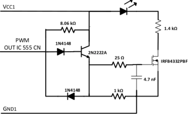
The gate-emitter voltage applied to the MOSFET is produced by pulse width modulation (PWM) from the output of the integrated circuit (IC) 555 CN. As the output of this IC cannot be connected directly to the MOSFET gate, an interface between the control signal and the power module is used, consisting in a bipolar transistor 2N2222A (Fig. 5).
1N4148 1N4148 8.06 k 25 1 k 2N2222A IRFB4332PBF 4.7 nF PWM OUT IC 555 CN 1.4 k VCC1 GND1
Figure 5 Interface between the control signal and the power MOSFET.
The diode 1N4148 connected between the emitter of the transistor and the PWM control signal allows to impose a zero voltage level to the MOSFET gate, thus blocking the MOSFET whenever the PWM signal goes low. When the PWM signal goes high, the other 1N4148 diode polarizes the base of the transistor, putting it in a conducting state, appearing in this way a high voltage signal at the emitter terminal.
This high voltage level will also appear at the gate of the MOSFET, putting it in a conducting state.
The 25 Ω resistor, connected between the emitter of the transistor and the gate of the MOSFET, mitigates the fluctuations due to the parasitic capacitance of the MOSFET gate, facilitating the switching operation. The 4.7 nF capacitor connected between the gate and the source of the MOSFET ensures the stabilization of the gate voltage.
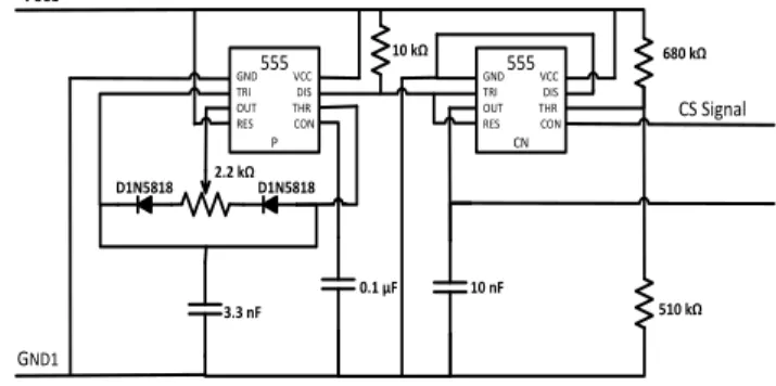
B. Pulse width modulation
For the production of the pulse width modulated control signal, two oscillators 555 are used, as shown in Fig. 6. The first, of P-type, can operate up to a maximum frequency of 500 kHz, and is configured as a stable oscillator. It will oscillate without any external trigger, in order to produce an intermediate PWM signal, with an adjustable duty-cycle with the aid of the 2.2 kΩ potentiometer.
To maintain a constant switching frequency, a special assembly was made, where the output of the PWM intermediate PWM signal is taken from the discharge pin of the IC 555P instead from its output pin. When the circuit in Fig. 6 is turned on, the trigger pin of the IC 555P is in a low voltage state, as the capacitor of 3.3 nF is discharged. This begins the oscillator cycle, causing the output pin to go into a high state. 2.2 kΩ 680 kΩ 510 kΩ 10 kΩ P CS Signal D1N5818 D1N5818 3.3 nF 0.1 µF 10 nF VCC1 GND1 555 GND VCC TRI DIS OUT THR RES CON P P 555 GND VCC TRI DIS OUT THR RES CON CN
Figure 6 Generation of the PWM control signal
As soon as the output goes high, the capacitor of 3.3 nF begins to charge through the left side of potentiometer 2.2 kΩ and the left diode D1N5818.
When the voltage at the capacitor of 3.3 nF reaches 2/3 of 12 V (VCC1=12 V), the
threshold pin is active, which in turn causes the output and discharge pins to go to a low voltage level. In the next step, the capacitor of 3.3 nF starts to discharge through the right side of potentiometer 2.2 kΩ and the right diode D1N5818. When the voltage at the capacitor of 3.3 nF drops below 1/3 of 12 V, the output and discharge pins go to a high voltage level and the cycle repeats.
The value of the charge and discharge resistor, set by the position of the potentiometer, influences the duty cycle of the intermediate PWM signal, but the period of this signal is always constant, as it is determined by the sum of the two resistors, which in Fig. 6 corresponds to the value of the potentiometer resistance. Thus, in the proposed circuit, the PWM frequency is maintained constant, whatever the duty cycle requested. The theoretical frequency of this intermediate PWM signal is given by [16]:
Frequency = 1.44/ (Output resistance*Capacity in the trigger and threshold pin). The discharge pin of IC 555P is connected to a resistor of 10 kΩ, and provides the intermediate PWM signal to drive the second oscillator, being connected to its trigger and reset pins.
The second 555 is of CN-type, and can oscillate up to a maximum frequency of 2.1 MHz. The output signal of this IC 555 CN is identical to its input (the intermediate PWM signal) if the control pin has a voltage greater than 5.1 V and a voltage near 0 V otherwise. The value of this threshold voltage (5.1 V in this design) is set by the voltage divider connected to the threshold pin, taking into account the following relations: 2 1+ 2 OUT in R V V R R (1)
Considering R1=680 kΩ, R2 =510 kΩ and Vin=12V, one obtains VOUT=5.1 V.
C. DC-DC converter control
Two main methods can be used for controlling the duty cycle of the DC-DC converter while keeping the output voltage within the desired range: the voltage control mode and the current control mode.
In the voltage control mode, the output voltage is measured and compared with the desired output voltage. An error is generated and amplified by a differential amplifier and then it may be used in a comparison with a ramp signal to produce the PWM signal [17].
The current control mode is implemented with the use of a sensing resistor or current sensor in the secondary side of the transformer, in series with the load (see Fig. 4). The current is measured and converted into a voltage signal being then compared with a reference voltage. The reference voltage corresponds to a previously converted current value (desired output current) [18]. An error signal is generated, and after being suitably conditioned by a differential amplifier, a hysteretic control signal is obtained producing the appropriate duty cycle [19].
The current control mode has greater flexibility with regard to limiting the output current, a faster response to load variations, and offers the possibility of connecting different DC-DC converters in parallel, with an easy management of the load sharing [20]. Having this in mind, it was decided to use a current control mode in the DC-DC converter here proposed.
The basic scheme of the designed current control system is shown in Fig. 7, where a proportional controller is used to accelerate the response of the system to variations in the reference (desired) output current.
CS Signal LM6171 ISO124 3.3 nF 15 Ω Output of DSPACE 2.4 kΩ 2.4 KΩ 39 KΩ 39 KΩ 22 KΩ 22 KΩ 20 nF VCC2 -VCC2 -+ VCC2 -VCC2 VCC3 -VCC3 GND2 GND3
The current supplied to the load by the DC-DC converter is measured with a CMS3005 Hall effect sensor that ensures the isolation between the secondary side of the flyback transformer and the control circuitry. This sensor has a very high bandwidth (2 MHz) and was connected in a serial configuration, allowing it to measure currents ranging from -5 A to 5 A. When this sensor is powered with ±15 V it provides an output voltage in the range of -10 V to 10 V. To reduce noise effects, a low pass-filter with a cut-off frequency of 3 MHz is connected at the output terminals of this current sensor.
A dSPACE platform generates a reference voltage signal between 0 V and 10 V, corresponding to the reference (desired) load current delivered by the DC-DC converter to the DC bus. The difference between the output voltage of the current sensor and the reference voltage given by dSPACE is detected by a differential amplifier LM6171 with a slew rate of 3600 V/μs and a bandwidth of 100 MHz, which also performs the amplification of the error signal. Considering an offset error of 1 mV (0.02% error) introduced by the output channels of dSPACE, and an error of 2.47% (247 mV) introduced by the current sensor (in extreme conditions), plus some safety margin, a maximum error of 250 mV was considered, which corresponds to an error of 250 mV/10000 mV=2.5%.
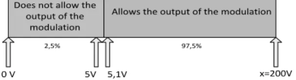
Knowing that the IC 555 CN, with a voltage lower than 5.1 V in the voltage control input does not generate any PWM signal in its output pin, one can draw the diagram shown in Fig. 8.
Does not allow the output of the
modulation
Allows the output of the modulation
0 V 5V 5,1V x=200V
2,5% 97,5%
Figure 8 Modeling a function for the voltage at the control input.
In practical terms, the LM6171 output voltage can never reach 15 V due to saturation. Considering, for the differential amplifier, an input resistance Re of 2.4 kΩ,
and the relation
2- 1
f O e R V V V R , (2)Where VO is the voltage in the output (200 V), V2 is the maximum voltage that
may be applied at the inputs (10 V) and V1 is the minimum voltage value at the inputs
(0 V), one obtains a value of Rf 48 k for the two output resistors of the differential amplifier.
The signal obtained at the output of LM6771 is then isolated with an ISO124 precision isolation amplifier configured with a unit gain, thus obtaining the control signal (CS signal) for the IC 555 CN.
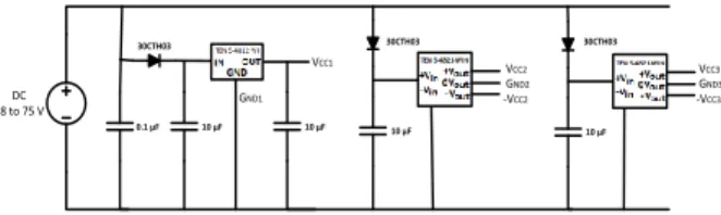
D. Auxiliary power supplies
An aspect that cannot be neglected is the power supply of all electronics needed for the generation of the control signals of the entire DC-DC converter. The three auxiliary voltages needed, VCC1, VCC2 and VCC3, are obtained with the aid of auxiliary
DC-DC converters, as shown in Fig. 9. The entire supply system may be fed from a variable input voltage in the range of 18-75 V.
DC 18 to 75 V VCC1 VCC2 GND2 -VCC2 VCC3 GND3 -VCC3 0.1 µF 30CTH03 30CTH03 30CTH03 10 µF 10 µF 10 µF 10 µF GND1
Figure 9 Auxiliary power supply
In Fig. 9, the diodes 30CTH03 prevent the current flow in reverse direction and the 10 μF capacitors on the left side of the auxiliary DC-DC converters ensure protection and voltage stabilization. The capacitor of 10 μF on the output side of TEN WI-4812, allows the stabilization of its output voltage around 12 V. This is important for the proper generation of the PWM signal by the two oscillators with a frequency of 200 kHz, whose value depends on the charge time and discharge time of the capacitor of 3.3 nF.
The current sensor CCMS3005, the differential amplifier LM61171 and the input stage of ISO124 are supplied with symmetrical voltages of Vcc2=±15 V, obtained with
the converter TEM 6-4823 WIN. It should be pointed out that this converter provides full isolation between the input and output sides.
The output stage of ISO124 is fed by a third auxiliary symmetrical voltage of
Vcc3=±15 V.
E. RC Snubber for the MOSFET
DC-DC converters with PWM have not an ideal behavior, leading to voltage and current waveforms with some oscillations that are primarily caused by the circuit parasitic capacitances. These oscillations must be adequately suppressed, as they can cause malfunctions or even the failure of the semiconductors (namely the MOSFET), if they reach high levels [21].
In the following, a set of theoretical methods and practical techniques for the design of a RC snubber circuit for the MOSFET are presented.
In a first step, the circuit was assembled without any snubber in parallel with the MOSFET and without the limiting RCD network for the transformer, whose design will be described in the next subsection.
The purpose of this test was to analyze the behavior of the voltage between the drain and the source of the MOSFET (VDF). In this test, the DC-DC converter was
supplied with 18 V, with a resistive load of 1 kΩ connected to its output. The voltage waveform corresponding to VDF was recorded with a Tektronix DPO 2014
oscilloscope, as shown in Fig. 10.
The large high-frequency oscillations visible in the waveform shown above occur due to the resonance between the inductance of the transformer and the parasitic capacitances of the circuit. The goal now is to eliminate these oscillations in order to prevent damages to the MOSFET, or even power oscillations on the transformer secondary side.
A RC snubber is connected between the drain and the source of the MOSFET, consisting in a series connection of a resistance, whose value must be chosen correctly to dissipate the energy associated with the ripple, and a capacitor to ensure that the power dissipated in the resistance is not excessive.
The sizing of the snubber components involves the measurement of inductance of the transformer. For this purpose, a BK PRECISION 889A LCR meter was used, with a short circuit is applied across the secondary of the transformer, and the impedance being measured from the primary side. A value of -9
= 93 10 H
L was obtained.
The ringing oscillation frequency was measured based on the VDF waveform (see
Fig. 10), being obtained a value of fr=12.5 MHz. The characteristic impedance of the
resonant circuit, given by Z=2πfrL, is 7.5 Ω. The ringing will be well damped if the
snubber resistance is set equal to the impedance of the resonant circuit R=Z. The resistance used in practice was 6.8 Ω (5 W), value available on the market.
The impedance of the capacitor at the ringing frequency should be set equal to the snubber resistance (C=1/(2πfrR)) [22]. Thus, the snubber capacitor C is chosen with
the value 1.74 nF. In practice, a value of 1.8 nF was used, which is available on the market.
The power dissipated in the snubber can be calculated by [22]: Psn=CV
2
fs (3)
Considering that a drain-to-source voltage of the MOSFET, in normal operation, less than 100 V, a capacitance C=1.8 nF and the switching frequency fs=200 kHz, a
power of Psn=3.6 W is calculated. In practice, a value of 5 W was chosen for the
power of the snubber resistor.
Fig. 11 shows the obtained results regarding the operation of the DC-DC converter with the designed RC snubber. Comparing these results with the ones shown in Fig. 10, it can be seen the effectiveness of this snubber, as the ringing is almost absent.
F. Primary RCD Clamp for Flyback Converter
An RCD clamp circuit is needed to absorb the energy stored in the transformer leakage inductance once the MOSFET drain voltage exceeds the clamp capacitor voltage.
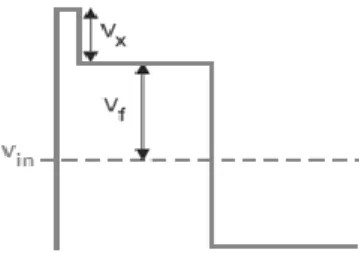
Even with a very light load level in the converter, the capacitor will always be charged up to the voltage reflected from the secondary side of the converter, Vf. As the load level increases, more energy will flow into the capacitor, and the voltage will rise by an additional amount, Vx, above the ideal square wave flyback voltage (Fig. 12).
The primary inductance of the transformer Lp@200 kHz is 42.855 μH. Since Ts
=1/(200x103) s, in order to avoid the converter to leave the discontinuous mode, one considered TON=0.48Ts=3.43×10⁻⁵ s.
Figure 12 Voltage in capacitor of the RCD limiter
The DC-DC converter to be designed is intended to have an output voltage Vdc=24
V. Hence, the peak primary current will be given by [22]
( -1) 1.29 A dc ON p P V T I L (4)
Considering a minimum input voltage Vin (min)=24 V, Vx50 V and 250 V
máx x
V ,
where máx x
V is the maximum avalanche voltage VDS of the MOSFET, one obtains
(min)
- - =176 V
máx
f x x in
V V V V (5)
The resistance can now be given by [20]:
max 2 2 ( 876.3 k ) x s f x sn p V T V V R LI (6)
In practice, a value of 860 kΩ was adopted.
The snubber capacitor must be able to maintain the voltage constant while absorbing energy, and may be calculated using the relation [23]:
, sn sn sn sn s V C V R f (7)
Where Vsn is the maximum allowed voltage variation, being normally set
between 5% and 10%. In this design, a value of 5% was considered.
The voltage Vsn can be seen from the secondary to the primary as 2.5×Vdc, where n
is the transformation ratio of the transformer. A value of CSn=1.03 μF is obtained, so
any value with higher capacity can be used. In the present design, a value of 75 μF was adopted.
The power dissipated in the RCD clamp circuit is given by 2 ( x f) sn V V P R , (8)
thus obtaining a value of 58.28 mW.
G. Output filter capacitor
An output filter should be used in the DC-DC converter in order to obtain a stabilized load voltage. In the flyback topology, the minimum output filter capacitor C0, is given
by [15]: 0 0 ( s- off) C I T T C V , (9)
where I0 is the maximum output current (considered as 2 A), toffis the blocking
time and VC is the allowed voltage variation in the capacitor, here considered as 5 mV. The value obtained for C0 is 960 μF. In the present design, a value of 2000 μF was
used in practice.
5. EXPERIMENTAL VALIDATION
A. Laboratory prototype
Following the design rules presented in the previous section, a prototype of the designed flyback DC-DC converter was constructed, as shown in Fig. 13.
Figure 13 Prototype of the flyback DC-DC converter.
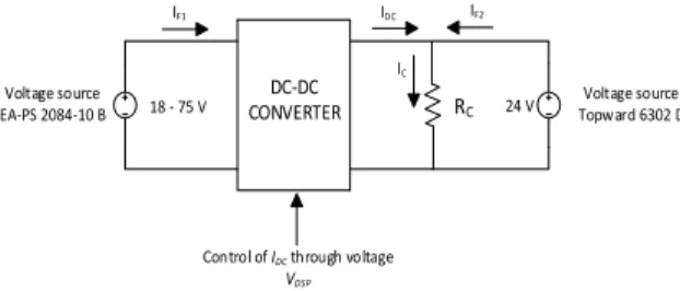
This DC-DC converter was then tested, according to the test setup shown in Fig. 14. 24 V DC-DC CONVERTER Voltage source EA-PS 2084-10 B Voltage source Topward 6302 D 18 - 75 V RC IF1 IDC IF2 IC
Control of IDC through voltage
VDSP
The input side of the DC-DC converter was connected to a voltage source of 24 V. To emulate the real working conditions of each DC-DC converter when integrated into the system shown in Fig. 1, a second voltage source of 24 V is connected to the output side of the DC-DC converter under test. The role of this voltage source is to impose a constant voltage to the common DC bus. Moreover, the output is also connected to a resistive load Rc =16 Ω. The reference value of the DC-DC converter
output current (IDC in Fig. 14) is controlled with the aid of an adjustable voltage
source, whose output signal will serve as the basis for controlling IDC. B. Experimental results
For each value of the adjustable voltage, different quantities were recorded, being presented in Table II.
As can be seen, the current IDC is almost proportional to the control voltage VDSP,
which is what could be anticipated from the design stage of the DC-DC converter.
TABLE II Behavior of the DC-DC Converter for Different Values of the Controlled Output Current Control VDSP (V) IF1 (A) IF2 (A) IDC (A) DC-DC converter efficiency (%) 0 0.08 1.49 0 0 0.1 0.09 1.48 0.01 11 0.2 0.09 1.47 0.02 23 0.3 0.18 1.42 0.07 39 0.4 0.42 1.25 0.23 57 0.5 0.59 1.12 0.37 62 0.6 0.82 0.96 0.53 65 0.7 1.15 0.74 0.72 63 0.8 1.47 0.63 0.84 57 0.9 1.78 0.49 0.98 55 1 2.21 0.27 1.15 52
The efficiency of this converter was also evaluated for different values of the output current, and it is shown in the last column of Table II.
Considering the operation of the DC-DC converter between 0 A and 1 A, its maximum efficiency is obtained typically in the range of 50-70 % of rated load.
Fig. 15 shows the input current and voltage waveforms obtained with the converter operating at 40 % of rated load. One can see that while the voltage remains approximately constant (it is imposed by the voltage source), the input current waveform resembles a sawtooth due to the operation of the converter in discontinuous mode.
Fig. 16 and Fig. 17 show the output voltage and current waveforms for two different DC-DC converter load levels. As can be seen, both waveforms are very stable and follow the expected values.
Figure 16 Output voltage and current waveforms for an output reference current of 0.5 A.
Figure 17 Output voltage and current waveforms for an output reference current of 1 A.
Having validated the good steady-state behavior of the constructed DC-DC converter, it is also important to test its dynamic behavior, namely its ability to track quickly the reference value of the output current. With this purpose, the reference voltage signal (which is proportional to the output reference current) is generated with the dSPACE platform and a current step with an amplitude of 1 A is imposed at t=0 s. The obtained results are shown in Fig. 18, and demonstrate that the converter only needs a few tens of milliseconds to reach the desired output current. Given the needs of the target application of this DC-DC converter, the response can be considered almost instantaneous.
Figure 18 Dynamic response time of the DC-DC converter for a reference current step of 1 A.
6. CONCLUSION
This paper presents a set of design criteria for building flyback DC-DC converters for the interconnection of different sources of renewable energy with energy storage elements and flexible load profiles to a common DC bus. This power system requires
-0.10 -0.05 0 0.05 0.1 0.15 0.2 0.25 0.3 0.2 0.4 0.6 0.8 1 1.2 Time (S) C ur re nt ( A )
the use of DC-DC converters with the ability to regulate the output power injected into the DC bus through the regulation of their output currents.
For this purpose, a prototype of the designed DC-DC converter was built and tested in the laboratory. The obtained results demonstrate a fast and accurate regulation capability of the output current through the use of a voltage control signal which, in practice, may be generated by an energy management system according to some specific algorithms.
The proposed DC-DC converter exhibits a very good dynamic behavior and a stable steady-state response, while ensuring isolation between its input side, output side and control circuitry.
The presented design methodology was validated experimentally and can be easily used in the design of flyback DC-DC converters for different purposes.
REFERENCES
[1] F. Andrén, B. Bletterie, S. Kadam, P. Kotsampopoulos, and C. Bucher, On the Stability of Local Voltage Control in Distribution Networks With a High Penetration of Inverter-Based Generation, IEEE Transactions on Industrial Electronics, Volume 62, pp. 2519–2529, 2015.
[2] D. Jovcic, M. Taherbaneh, J. P. Taisne, and S. Nguefeu, Developing regional, radial DC grids and their interconnection into large DC grids, in PES General Meeting | Conference & Exposition, 2014 IEEE, 2014, pp. 1–5.
[3] Switch Mode Power Supply Topologies Compared, W. E. Midcon, Ed., ed. Waldenburg, Germany, 2016.
[4] F. L. Luo and H. Ye, Advanced DC/DC Converters: CRC Press, 2003. [5] S. Maniktala, Switching Power Supplies A to Z. Burlington, USA, 2006.
[6] S. Maniktala, Troubleshooting Switching Power Converters. Burlington, USA: Elsevier, 2008.
[7] Y. C. Hsieh, M. R. Chen, and H. L. Cheng, An Interleaved Flyback Converter Featured With Zero-Voltage Transition, IEEE Transactions on Power Electronics, 26, pp. 79–84, 2011.
[8] J. W. Shin, S. J. Choi, and B. H. Cho, High-Efficiency Bridgeless Flyback Rectifier With Bidirectional Switch and Dual Output Windings, IEEE Transactions on Power Electronics, 29, pp. 4752–4762, 2014.
[9] F. Forest, Laboure, x, E., T. A. Meynard, and J. J. Huselstein, Multicell Interleaved Flyback Using Intercell Transformers, Power Electronics, IEEE Transactions on, 22, pp. 1662–1671, 2007.
[10] W. Dong, H. Xiangning, and S. Jianjiang, Design and Analysis of an Interleaved Flyback– Forward Boost Converter with the Current Autobalance Characteristic, Power Electronics, IEEE Transactions on, 25, pp. 489–498, 2010. [11] M. Brown, Power Sources and Supplies. Newnes, 2007.
[12] Z. Zhiliang, H. Xiao-Fei, and L. Yan-Fei, An Optimal Control Method for Photovoltaic Grid-Tied-Interleaved Flyback Microinverters to Achieve High Efficiency in Wide Load Range, Power Electronics, IEEE Transactions on, 28, pp. 5074–5087, 2013.
[13] J. Young-Hyok, J. Doo-Yong, K. Jae-Hyung, L. Tae-Won, and W. Chung-Yuen, A current shaping method for PV-AC module DCM-flyback inverter under CCM operation, in Power Electronics and ECCE Asia (ICPE & ECCE), 2011 IEEE 8th International Conference on, 2011, pp. 2598–2605.
[14] C. Kai-Hui and L. Tsorng-Juu, Design of Quasi-resonant flyback converter control IC with DCM and CCM operation, in Power Electronics Conference (IPEC-Hiroshima 2014 - ECCE-ASIA), 2014 International, 2014, pp. 2750–2753. [15] K. B. Abraham I. Pressman, Taylor Morey, Switching Power Supply Design.
USA: McGraw-Hill, 2009.
[16] LM555 Timer, ed. USA: National Semicondutor Corporation, 2006.
[17] R. Mammano, Switching Power Supply Topology Voltage Mode vs. Current Mode, ed. MERRIMACK, NH 03054: Texas Instruments Incorporated, 1999. [18] H. Martinez-Garcia and A. Grau-Saldes, A linear-assisted DC/DC converter
based on current-mode control, in Emerging Technology and Factory Automation (ETFA), 2014 IEEE, 2014, pp. 1–8.
[19] C. Chia-Jung and C. Chern-Lin, An Isolated Output-Feedback Scheme With Minimized Standby Power for SMPS, Power Electronics, IEEE Transactions on, 28, pp. 5140–5146, 2013.
[20] M. Kamil, Switch Mode Power Supply (SMPS) Topologias, ed: Microchip Technology Inc., 2007.
[21] T. E. Salem, C. W. Tipton, and D. Porschet, Fabrication and Practical Considerations of a Flyback Transformer for Use in High Pulsed-Power Applications, in System Theory, 2006. SSST '06. Proceeding of the Thirty-Eighth Southeastern Symposium on, 2006, pp. 406-409.
[22] D. R. Ridley. (2005, 2005) Flyback Converter Snubber Design. Switching Power Magazine. Available: http://pt.scribd.com/doc/54919306/Snubber-Design-Dr-ray-Ridley.
[23] Anu R and Reshmila .S, Modelling of High Step Up DC-DC Converter For Photovoltaic Modules. International Journal of Electrical Engineering &
Technology, 5(12), 2014, pp. 227–232.
[24] Aswathy Haridas, Saritha K.S and Ajith K.A, New ZV/ZCS Full Bridge DC-DC Converter with Fuzzy & Pi Control . International Journal of Electrical Engineering & Technology, 5(12), 2014, pp. 156–169.
[25] Indulekha Sajeev and Shemi P A, Bidirectional Full-Bridge DC-DC Converter with Flyback Snubber for Photovoltaic Applications. International Journal of
Electrical Engineering & Technology, 5(12), 2014, pp. 233–239.
[26] G.-B. K. P. D. (2006, Design Guidelines for RCD Snubber of Flyback Converters. Available: http://www.fairchildsemi.com/an/AN/AN-4147.pdf
![Table I shows a comparison of the most common types of DC-DC converters [3- [3-6].](https://thumb-eu.123doks.com/thumbv2/123dok_br/15761983.1074923/3.893.94.808.738.1010/table-shows-comparison-common-types-dc-dc-converters.webp)
![Fig. 2 shows the topology of a flyback converter [10]. Initially, the power switch is closed to allow the circulation of current in the primary circuit of the transformer, being the energy stored in its magnetic circuit](https://thumb-eu.123doks.com/thumbv2/123dok_br/15761983.1074923/4.893.268.609.421.574/topology-flyback-converter-initially-circulation-current-transformer-magnetic.webp)