Abstract— We present a microwave switchable frequency selective
surface with high quality factor transmission resonance. The high quality resonance is achieved by excitation of the trapped-mode in array with two concentric metal rings in a cell on a silicon substrate. Optical activation of the silicon substrate permits to switch off the transmission band.
Index Terms— Frequency selective surface, high quality factor resonance, trapped-mode resonance, optical activation.
I. INTRODUCTION
Control of microwave propagation by a boundary surface or a layer is a subject of intense
investigation in applied electrodynamics. Arrays of patches or aperture elements can have a great
versatility of electromagnetic responses. Unusual applications of these arrays in microwave region
include invisibility metal [1], magnetic mirror [2-3], optical activity [4], thin electromagnetic
absorbers [5] and reconfigurable antennas [6]. In terahertz region, applications related to wave
manipulation and sensing have been also reported [7-8].
In this work we propose a switchable FSS with high quality factor (Q-factor) transmission
resonance controllable by optical activation of its silicon substrate. This structure can be used in
antennas and waveguide technologies, and in electromagnetic compatibility systems, for example, in
active filters. The high Q-factor resonance is achieved by excitation of the so-called trapped-mode
regime in array where every cell is formed by two concentric rings. This array pattern was originally
proposed in [9].
The trapped-mode is defined by excitation of anti-symmetric currents in the rings. This mode is
weakly coupled to free-space, therefore the radiation losses are low and the Q-factor is very high as
compared with a conventional resonance mode [10]. The Q-factor of presented FSS is around 8 while
that of a similar FSS with a single ring resonant element is around 1 (we define the Q-factor as the
Microwave switchable frequency selective
surface with high quality factor resonance and
low polarization sensitivity
Victor Dmitriev and Marcelo N. Kawakatsu
rotational symmetry, this array is polarization independent for normal incidence [11]. We have chosen
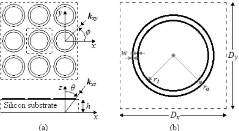
the dimensions of the array shown in Fig. 1 in accordance with the results of [12], where a study of
the influence in trapped-mode resonance with substrate loss and rings dimensions was made. The
following values of geometrical parameters were considered in the simulations for obtaining a
trapped-mode resonance around 40 GHz: Dx = Dy = 1.3, ro = 0.6, ri = 0.5, w = 0.02 and h = 0.05 (all
dimensions in mm).
Fig. 1. FSS consisting of array of two concentric rings supported by silicon substrate (a) and unit cell of the array (b).
In our simulations the array of metal rings made of perfect conductors is considered to be infinite in
x- and y-directions. The optically activated silicon substrate was modeled as in [13], in which the
relative permittivity of the silicon can be described in the form
2 2
2 2 2 2
p p
r p
v
j
v
v
ω
ω
ε
ε
ω
ω ω
=
−
−
+
+
(1)where εp is the dielectric constant of the silicon in passive state,
2 2 *
0
/
p Ne m
ω
=ε
is the plasmafrequency, v is the collision angular frequency, N is the plasma density, e is the electron charge, m* is
the effective mass of the charge carrier and ε0 is the free-space permittivity. Since the optically
activated silicon substrate behaves as a semiconductor containing electron-hole pairs, it is necessary
in Eq. (1) to take into account the contributions of electrons and holes separately as described in [13].
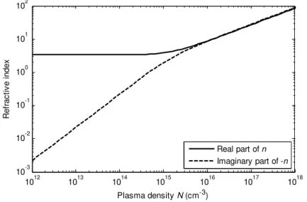
Using the same numerical values given in [13], we calculated the behavior of the complex refractive
1012 1013 1014 1015 1016 1017 1018 10-3
10-2 10-1 100 101 102
Plasma density N (cm-3)
R
ef
rac
ti
v
e i
ndex
Real part of n
Imaginary part of -n
Fig. 2. Refractive index of the silicon substrate as a function of the plasma density N.
III. NUMERICAL RESULTS
For numerical calculation of the reflection and transmission characteristics, we used the
well-established spectral domain moment method (SDMM) which consists in solving by method of
moments the integral equation of the problem in the frequency domain [14]. In this method, the
periodic boundary conditions are taken into account by considering only harmonics of the components
kx and ky of the wavenumber which follows from the periodicities of the array in the x- and
y-directions. The substrate was modeled by the Green’s function obtained by applying the boundary
conditions on the top and the bottom interfaces of the substrate. The surface current density on the
rings was modeled using the roof-top subdomain basis functions. For validating our results, we used
the commercial software Computer Simulation Technology (CST) [15], which is based on the finite
integration technique.
In Fig. 3 are shown the reflection, transmission and normalized absorption frequency responses for
N = 1014 cm-3 calculated using SDMM and CST, demonstrating good agreement between the results.
In Fig. 4 the reflection and transmission curves of the array for normally incident plane wave and
different values of N are shown. These graphics were obtained with SDMM. For N = 1012 cm-3, the
influence of plasma on the refraction index of the silicon substrate is negligible and a high Q-factor
transmission resonance exists with almost total transmission at 40 GHz. Note that the trapped-mode
resonance is between two broad reflection resonances, which are generated by the outer and inner
10 20 30 40 50 60 70 80 90 100 0
0.2 0.4 0.6 0.8 1
Frequency (GHz)
C
o
e
ffi
c
ie
n
ts
Reflection
Transmission
Absorption
Figure 3. Reflection and transmission frequency responses of FSS for normal incidence and N = 1014 cm-3, calculated using
SDMM (solid-curve and dotted-curve) and CST (dashed-curve).
In Fig. 5 the reflection and transmission curves are shown for inclined incidence with φ = 0°, θ =
30°, N = 1012 cm-3 and for TE- or TM-polarizations. For the TE case, the Q-factor of the
trapped-mode resonance is a little bit higher and the adjacent reflection resonances are broadened in
comparison with the normal incidence. For the TM case, the opposite behavior is observed. The small
peaks and deeps near 80 GHz are due to grating lobes. Our analysis shows that due to the high
rotational symmetry of the array unit cell, the responses are almost insensitivity to the angle φ.
Figure 5. Reflection and transmission frequency responses of FSS for incidence with φ = 0° and θ = 30°, N = 1012 cm-3, and TE- or TM-polarization.
IV. CONCLUSION
We suggested and analyzed a switchable FSS with high Q-factor transmission resonance and low
polarization sensitivity. The analyzed FSS has the Q-factor about 8, which is much higher than that of
similar FSS with a single ring resonant element. High Q-factor is achieved due to excitation of the
trapped-mode. Using an optically activated silicon substrate, we demonstrated theoretically that it is
possible to switch on and off the transmission band. The frequency band of the structure can be scaled
to lower or higher frequencies.
ACKNOWLEDGMENTS
This work was financially supported by the Brazilian agencies CNPq and CAPES.
REFERENCES
[1] V. A. Fedotov, P. L. Mladyonov, S. L. Prosvirnin, and N. I. Zheludev, “Planar electromagnetic metamaterial with a fish
scale structure”, Phys. Rev. E, vol. 72, November 2005.
[2] D. Sievenpiper, L. Zhang, R. F. J. Broas, N. G. Alexopolous, E. Yablonovitch, “High-impedance electromagnetic
surfaces with a forbidden frequency band”, IEEE Trans. Microw. Theory Tech., vol. 47, issue 11, pp. 2059−2074,
November 1999.
[3] M. Hosseini, A. Pirhadi, and M. Hakkak, “A novel AMC with little sensitivity to the angle of incidence using 2-layer
Jerusalem Cross FSS”, Progress In Electromagnetics Research, vol. 64, pp. 43-51, 2006.
[4] E. Plum, V. A. Fedotov, and N. I. Zheludev, “Optical activity in extrinsically chiral metamaterial”, App. Phys. Lett.,
[9] N. Papasimakis, Y. H. Fu, V. A. Fedotov, S. L. Prosvirnin, D. P. Tsai, and N. I. Zheludev, “Metamaterial with polarization and direction insensitivity resonant transmission response mimicking electromagnetically induced
transparency”, Appl. Phys. Lett., vol. 94, 211902, 2009.
[10]V. A. Fedotov, M. Rose, S. L. Prosvirnin, N. Papasimakis, and N. I. Zheludev, “Sharp Trapped-Mode Resonance in
Planar Metamaterials with a Broken Structural Symmetry”, Phys. Rev. Lett., vol. 99, issue 14, October 2007.
[11]V. Dmitriev, “Symmetry properties of electromagnetic planar arrays: Long-wave approximation and normal incidence”,
Metamaterials Congress 2010, vol. 5, issue 2-3, pp. 141−148, September 2011.
[12]M. N. Kawakatsu, V. A. Dmitriev, and S. L. Prosvirnin, “Microwave Frequency Selective Surfaces with High Q-Factor
Resonance and Polarization Insensitivity”, Journal of Electromagnetic Waves and Applications, vol. 24, pp. 261−270,
2010.
[13]C. H. Lee, P. S. Mak, and A. P. De Fonzo, “Optical Control of Millimeter-Wave Propagation in Dielectric
Waveguides”, IEEE J. Quantum Electron., vol. E-16, no. 3, March 1980.
[14]R. Mittra, C. H. Chan and T. Cwik, “Techniques for Analyzing Frequency Selective Surfaces – A Review”,
Proceedings of the IEEE, pp. 1593–1615, 1988.