RUI MIGUEL DOS SANTOS MARTINS
IN-SITU
X-RAY DIFFRACTION STUDIES DURING GROWTH
OF Ni-Ti SHAPE MEMORY ALLOY FILMS AND THEIR
COMPLEMENTARY
EX-SITU
CHARACTERIZATION
Thesis submitted to the Faculty of Sciences and
Technology of the New University of Lisbon for the
degree of Doctor in Materials Engineering-
Metallurgical Technologies.
This thesis was prepared in the framework of the
collaboration between the Forschungszentrum
Dresden-Rossendorf (FZD) and CENIMAT/FCT/UNL
in the Rossendorf Beamline (ROBL) at the European
Synchrotron Radiation Facility (ESRF) and at FZD.
The research work described in this thesis was carried out at the Forschungszentrum Dresden-Rossendorf (Institute of Ion Beam Physics and Materials Research / Rossendorf Beamline), and I would like to acknowledge all those people who helped to make this thesis possible. I am indebted especially to a number of people for scientific, theoretical, experimental, and moral support:
Firstly, many thanks to my supervisor Professor Francisco Manuel Braz Fernandes, my official supervisor at FCT/UNL. We were always in touch and I knew I always could come and discuss or ask him for help. His door was always open for discussions on both scientific and personal issues. I believe that this is the best what a student could have from the supervisor. Additionally he has initiated the international collaborations, which were indispensable in the success of this thesis.
I must give a special acknowledgement also to my supervisor Dr. Norbert Schell. Without his support, I would not have never came to FZD and made my PhD study. I am very grateful for all time that we have spent together. I am impressed by his ultimate patience and devotion for excellence. All these years spent with him were very enriching from both personal and professional point of view. I am grateful to Norbert for all that hard work he has done while working with me and trying to understand my way of thinking and being. He has been and is a true friend.
I would like to thank the FZD for funding my PhD work and the Portuguese Foundation for Science and Technology (FCT/MCTES) for a PhD individual grant since March 2006 (POCI 2010/FSE).
It is particular a pleasure for me to thank Dr. Johannes Borany, head of the Department for Structural Studies (FWIS), for the fruitful stays in Dresden. He provided excellent conditions, candid support and encouragement during this work.
I owe a huge debt of gratitude to Dr. Arndt Mücklich for engaged TEM analysis, for answering all my questions regarding the TEM technique and, especially, for his kindness and support during my stays at FWIS. For TEM observations it has also been essential the technical support given by Frau Martina Missbach and Frau Annette Kunz on the preparation of the samples for X-TEM. They have performed a great work.
I would like to thank Dr. Helfried Reuther and Frau Elfi Christalle for the technical support during SEM analyses carried out on my samples as well as their kind support during my stays at the department.
I am also grateful to Frau Elke Quaritsch for the big amount of AES measurements performed on my samples.
I would like to acknowledge the support of Dr. Frank Eichhorn who was an invaluable source of knowledge concerning XRD. I appreciate his time and patience with our measurements at the FWIS XRD laboratory. I would also like to thank Frau Andrea Scholz for all the XRD measurements that she performed for me in Dresden when I was working on different tasks in Grenoble. She was always very kind to me.
I must mention here the support of Dr. Shengqiang Zhou when, just before a beamtime at ROBL, I needed some RBS measurements. Shengqiang immediately performed the work at FZD and sent me the fitted data to ESRF. His wife was just living the last days of her pregnancy.
I would also like to acknowledge the support of other members of our group in Dresden, who have made my experience at FZD truly special: Dr. Kurt Walther, Frau Birgit Gebauer, Dr. Natalia Shevchenko, Joachim Kreher, Dr. Jörg Grenzer, Dr. Friedrich Prokert, Rene Weidauer.
Winfried Oehme and Siegfried Dienel, from the Department of Research Technology (at FZD), involved in the scientific and technical programme of ROBL, were responsible for technical improvements that led to successful beamtimes.
resulted on a very nice observation of the phase transformation characteristics as a function of the processing parameters. Dr. Karimbi Mahesh went several times to Grenoble to give precious support during the beamtimes. Dr. Andersan Paula was always somehow present when I needed her. Márcia Silva has been in Grenoble during the first beamtime for my PhD thesis work. I cannot forget her important support. They are much more than colleagues - they are good friends.
My deepest gratitude to Dr. Carla Santos who gave me confidence in my abilities during the thesis writing.
Shape Memory Alloy (SMA) Ni-Ti films have attracted much interest as functional and smart materials due to their unique properties. However, there are still important issues unresolved like formation of film texture and its control as well as substrate effects. Thus, the main challenge is not only the control of the microstructure, including stoichiometry and precipitates, but also the identification and control of the preferential orientation since it is a crucial factor in determining the shape memory behaviour.
The aim of this PhD thesis is to study the optimisation of the deposition conditions of films of Ni-Ti in order to obtain the material fully crystallized at the end of the deposition, and to establish a clear relationship between the substrates and texture development. In order to achieve this objective, a two-magnetron sputter deposition chamber has been used allowing to heat and to apply a bias voltage to the substrate. It can be mounted into the six-circle diffractometer of the Rossendorf Beamline (ROBL) at the European Synchrotron Radiation Facility (ESRF), Grenoble, France, enabling an in-situ characterization by X-ray diffraction (XRD) of the films during their growth and annealing. The in-situ studies enable us to identify the different steps of the structural evolution during deposition with a set of parameters as well as to evaluate the effect of changing parameters on the structural characteristics of the deposited film. Besides the in-situ studies, other complementary ex-situ characterization techniques such as XRD at a laboratory source, Rutherford backscattering spectroscopy (RBS), Auger electron spectroscopy (AES), cross-sectional transmission electron microscopy (X-TEM), scanning electron microscopy (SEM), and electrical resistivity (ER) measurements during temperature cycling have been used for a fine structural characterization.
O fabrico de películas finas de ligas Ni-Ti com memória de forma tem atraido especial interesse na área dos materiais funcionais e inteligentes, sobretudo devido às suas características peculiares. No entanto, existem ainda questões importantes que requerem resolução, como a identificação dos diferentes factores que influenciam o tipo de orientação preferencial da película depositada, um possível controlo da mesma, bem como a influência do tipo de substrato utilizado. Deste modo, não só se apresentam como factores preponderantes aqueles mais vezes mencionados (o controlo da microstrutura, incluíndo estequiometria e formação de precipitados), mas também se apresenta com particular ênfase, a identificação e controlo do tipo de orientação preferencial das películas de Ni-Ti, uma vez que, no caso das aplicações recorrendo ao efeito de memória de forma, existe uma relação entre a textura e a extensão da deformação recuperável.
Este trabalho teve por finalidade estudar as condições de optimização da produção (por pulverização catódica) de películas finas de Ni-Ti com memória de forma, de modo a obter material cristalino durante o processo de deposição (sem tratamentos térmicos adicionais), e sobretudo estabelecer uma relação entre o tipo de substrato usado e a evolução da orientação preferencial das películas. De forma a atingir este objectivo, foi utilizada uma câmara de deposição que permite a co-deposição a partir de dois alvos, bem como a deposição em substrato aquecido e polarizado. Este equipamento foi especialmente projectado para poder ser montado no círculo ϕ do goniómetro de 6 círculos existente na Rossendorf Beamline (ROBL), no European Synchrotron Radiation Facility (ESRF), permitindo assim a caracterização do processo de deposição por difracção de raios-X (DRX) in situ.Este tipo de estudo permite, por isso, acompanhar a evolução estrutural da película à medida que o processo de deposição vai avançando, bem como correlacionar as condições de deposição (fixas ou variáveis) com a microestrutura final da película. Após o processo de deposição, as películas foram estudadas ex situ, recorrendo-se a ensaios de DRX a nível laboratorial, espectroscopia de retrodispersão de Rutherford (RBS), espectroscopia electrónica de Auger (AES), microscopia electrónica de transmissão (TEM – amostras preparadas em secção transversal), microscopia electrónica de varrimento (SEM) e medidas da resistividade eléctrica durante ciclos térmicos, o que permitiu uma caracterização estrutural mais fina das películas.
Les couches minces en Alliage à Mémoire de Forme (AMF) Ni-Ti ont attiré l’intérêt comme matériaux intelligent et adaptatif grâce à leurs propriétés uniques. Cependant il y a encore de nombreuses difficultés non résolues comme la formation texture et son contrôle dans les couches minces ainsi que les effets du substrat. Donc le principal challenge n’est pas seulement le contrôle de la microstructure, incluant la stoechiométrie et les précipités mais aussi l’identification et le contrôle des orientations préférentielles puisqu’elles sont un facteur crucial pour déterminer le comportement de la forme mémorisée.
L’objectif de ce travail de thèse est d’étudier l’optimisation des conditions de dépôt de couches minces de Ni-Ti dans le but d’obtenir un matériau entièrement cristallisé et d’établir un lien évident entre le substrat utilisé et le développement de la texture. Pour accomplir cet objectif une chambre de dépôts par pulvérisation magnétron (à 2 cibles) permettant de chauffer et d’appliquer une tension sur le substrat a été utilisée. Cette chambre peut être monté sur le diffractomètre à 6-axes de la ligne de lumière de Rossendorf (ROBL) à l’European Synchrotron Radiation Facility (ESRF) à Grenoble, France. Cette installation permet de caractériser in-situ par diffraction de rayon X les couches minces pendant leur croissance et recuit. Les études in-situ nous permettent soient d’identifier les différentes étapes de l’évolution structurale pendant les dépôts avec des paramètres fixés, soient d’évaluer l’effet du changement des paramètres sur les caractéristiques structurales des couches minces déposées. A la suite de ces études in-situ, d’autres techniques complémentaires ex-situ ont été utilisées pour une caractérisation plus fine. Ces techniques sont la diffraction de rayons X de laboratoire, la spectrométrie de rétrodiffusion Rutherford (RBS), la spectrométrie par électrons Auger (AES), la microscopie à transmission (X-TEM), à balayage (SEM) et les mesures de résistance électrique pendant des cycles thermiques.
α deposition angle (relative to the substrate normal)
a0 lattice parameter
AES Auger electron spectroscopy
αf expansion coefficients of the film
Af austenite-finish temperature
As austenite-start temperature
αs expansion coefficients of the substrate
β angle of orientation of the film columns (relative to the substrate normal)
B19' martensite
B2 austenite
BF bright field
CEFITEC Centro de Física e Investigação Tecnológica CENIMAT Centro de Investigação de Materiais
d interplanar distance
DC direct current
DCM double-crystal monochromator
DF dark field
DSC differential scanning calorimetry
E Young’s modulus
EDX energy dispersive X-ray spectroscopy ER electrical resistivity
ESRF European Synchrotron Radiation Facility FZD Forschungszentrum Dresden-Rossendorf
GIXD X-ray diffraction in grazing incidence geometry off-plane GIXS grazing exit in-plane large angle scattering
GP Guinier-Preston
h distance target/substrate
HR high resolution
IBA ion beam analysis
IC integrated circuit
k Boltzmann constant
l mean free path
λ wavelength
MC Monte Carlo
MD molecular dynamics
MEMS micro-electro-mechanical system Mf martensite-finish temperature
MRH Materials Research Hutch
Ms martensite-start temperature
ν Poisson ratio
PVD phase vapour deposition
RF radio frequency
R’f R-phase-finish temperature on heating
R’s R-phase-start temperature on heating
RBS Rutherford backscattering spectroscopy Rf R-phase-finish temperature on cooling
RHEED reflection high-energy electron diffraction
ROBL Rossendorf beamline
Rs R-phase-start temperature on cooling
RT room temperature
σ cross section for the collision SAED selected area electron diffraction
SE superelasticity
SEM scanning electron microscopy
SMA Shape Memory Alloy
SME shape memory effect
σth thermal stress
T temperature
Td deposition temperature
TEM transmission electron microscopy
Tm melting temperature
UHV ultra high vacuum
Vb substrate bias voltage
XRD X-ray diffraction
XRR X-ray reflectivity
Introduction ... 2
1. Background and literature review ... 7
1.1. Ni-Ti shape memory alloy ... 7
1.1.1. Phase diagram and crystal structures ... 9
1.1.2. Shape memory effect (SME) and superelasticity effect (SE) ... 14
1.2. Thin films in general ... 17
1.2.1. Sputtering process ... 19
1.2.2. Growth and morphology ... 22
1.2.3. Energetic ion bombardment ... 28
1.2.4. Stress in the films ... 31
1.2.5. Texture in films ... 34
1.2.5.1. Types of texture ... 35
1.2.5.2. Driving forces ... 37
1.2.5.3. Examples of texture selection on amorphous or polycrystalline substrates .... 38
1.2.5.4. Examples of texture selection on single crystal substrates ... 42
1.3. Sputter deposition and microstructural details of Ni-Ti films ... 44
1.3.1. Composition control ... 46
1.3.2. Heat treatments ... 51
1.3.3. Oxidation ... 61
1.3.4. Interfacial film/substrate reactions ... 64
1.3.5. Film thickness effects ... 67
1.3.6. Texture ... 69
1.3.7. Ternary system NiTiHf ... 73
2. Experimental details ... 77
2.1. Film deposition and XRD characterization at ROBL ... 78
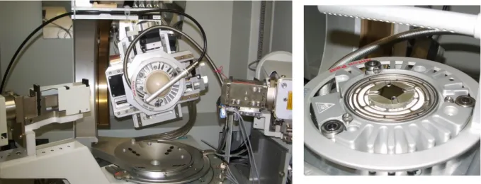
2.1.1 Materials Research Hutch: diffractometer and sputtering chambers ... 80
2.1.2. Experimental parameters at ROBL ... 85
2.2. Ex-situ XRD characterization ... 90
2.3. Rutherford backscattering spectroscopy (RBS) ... 92
2.4. Auger electron spectroscopy (AES) ... 93
2.5. Cross-sectional transmission electron microscopy (X-TEM) ... 94
2.6. Scanning electron microscopy (SEM) ... 96
2.7. Electrical resistivity (ER) measurements ... 97
3. Results ... 100
3.1. Near equiatomic Ni-Ti films grown on naturally oxidized Si substrates ... 100
3.1.1. In-situ experiments ... 101
3.1.2. Ex-situ characterization ... 105
3.2. Near equiatomic Ni-Ti films grown on thermally oxidized Si(100) substrates ... 111
3.2.1. In-situ experiments ... 111
3.2.2. Ex-situ characterization ... 115
3.3. Near equiatomic Ni-Ti films grown on a TiN buffer layer ... 124
3.3.1. In-situ experiments ... 125
3.3.1.1. Effect of the TiN crystallographic orientation on the development of Ni-Ti B2 phase ... 125
3.3.1.2. Effect of the substrate bias voltage on the structure of Ni-Ti films deposited on TiN ... 128
3.3.2. Ex-situ characterization ... 131
TiN ... 134
3.4. Near equiatomic Ni-Ti films grown on MgO single crystal substrate ... 139
3.4.1. In-situ experiments ... 139
3.4.1.1. Ni-Ti deposited directly on MgO single crystals ... 139
3.4.1.2. Ni-Ti deposited on TiN(100)/MgO(100) ... 142
3.4.2. Ex-situ characterization ... 144
3.4.2.1. Ni-Ti deposited directly onto MgO single crystals ... 144
3.4.3. Deposition of a TiN film with a topmost layer formed mainly by <100> oriented grains ... 148
3.5. Controlled change of the Ti:Ni ratio during the deposition of Ni-Ti films ... 153
3.5.1. Deposition on naturally oxidized Si(100) substrates ... 153
3.5.1.1. In-situ experiments ... 153
3.5.1.2. Ex-situ characterization ... 155
3.5.2. Deposition on TiN/SiO2/Si(100) substrates ... 162
3.6. Deposition of high-temperature NiTiHf SMA films ... 166
3.6.1. Study of the power applied to the magnetrons on the film composition ... 166
3.6.2. In-situ XRD results ... 167
4. Discussion ... 172
4.1. Preferential orientation ... 173
4.1.1. Effect of a SiO2 buffer layer ... 173
4.1.2. Deposition on MgO single crystal ... 174
4.1.3. Effect of a TiN buffer layer ... 175
4.1.4. Shadowing effects ... 178
4.1.5. Study of Ni-Ti graded films ... 180
4.1.6. Deposition of NiTiHf films ... 183
4.2. Interface analysis and phase transformation characteristics ... 184
4.2.1. Interface morphology ... 184
4.2.2. Variation of the Ni-Ti lattice parameter values ... 187
4.2.3. Phase transformation characteristics ... 191
5. Conclusions and future works ... 202
5.1. Conclusions ... 202
5.2. Future works ... 203
References ... 209
APPENDIX A. Properties of NiTiNOL ... 222
APPENDIX B. JCPDS cards (and simulations) used for the identification of the crystalline phases ... 224
Fig. 1.1: Power/weight ratio versus weight for SMA actuators as compared with other devices,
demonstrating the relatively large output of SMA actuators given their small size [9]. ... 8
Fig. 1.2: Phase diagram of a Ni-Ti alloy to which the phase equilibrium between the B2 and Ni4Ti3 phases are added. [1]. ... 9
Fig. 1.3: TTT diagram describing aging behaviour for Ti-52 at% Ni [11]. ... 10
Fig. 1.4: (a) B2 austenite phase, (b) B19’ martensite phase [14]. ... 11
Fig. 1.5: Transformation of cubic (B2) austenite to rhombohedral (R) phase [17]. ... 12
Fig. 1.6: Ms as a function of Ni content for binary Ni-Ti SMA. The different symbols represent data from different authors and the solid line is given by thermodynamic calculations [18]. ... 13
Fig. 1.7: Temperature dependence of electrical resistivity of a Ni-Ti sample, heat-treated at 380°C, in a complete thermal cycle [19]. ... 14
Fig. 1.8: (a)-(c) Schematic illustration of the mechanism of the SME and SE. The solid lines represent the SME and the dotted lines represent the SE path [1]. ... 15
Fig. 1.9: Free-standing film after crystallization exhibiting the two-way SME; (a) flat on a table, (b) bent after phase transformation on a human hand, (c) again flat on the table [27]. ... 17
Fig. 1.10: Scheme of the sputtering deposition process [34]. ... 19
Fig. 1.11: Overview of an unbalanced miniature magnetron, commercially available from AJA International [37] (type A4001) and a detail of the localization of the target (Ti target in the photo). ... 22
Fig. 1.12: Schematic illustration of the film growth process: atomic-scale phenomena affecting nucleation and growth [34]. ... 23
Fig. 1.13: Diagram of structural zones revealed as a function of the base temperature [39]. ... 24
Fig. 1.14: (a) Microstructure zone diagram for metal films deposited by magnetron sputtering showing the influence of the deposition pressure and homologous temperature on the morphology of films (T is the substrate temperature and Tm is the melting point of the coating material) [40]. (b) Main characteristics of structure zones used in the literature [41]. ... 25
Fig. 1.15: Model of the modification of the growth mode of a film by ion bombardment [47]. ... 30
Fig. 1.16: Plan-view, bright-field under-focused TEM image of a Ag film as deposited at −250 V bias showing white Ar bubbles [48]. ... 31
Fig. 1.17: Sequence of events leading to (a) residual tensile stress in the film, (b) residual compressive stress in the film [50]. Bending of a film/substrate compound induced by biaxial stress in the thin film. ... 32
Fig. 1.18: Pole figures; (a) Permalloy (Ni80Fe20) film exhibiting a strong <111> fibre texture [64], (b) (200) pole figure for a MgO film (without substrate rotation - the direction of the vapour flux is shown by the arrow) [62] (c)(200) pole figure for TiN/TiAlN multilayer coating deposited on WC-Co (with substrate rotation) [63]. ... 36
Fig. 1.19: Evolutionary selection during growth starting from randomly orientated equidistant nuclei on a one-dimensional substrate (bottom line) in a two-dimensional space. The height above the substrate is expressed in the unit ∆x, the distance between two nuclei. The assumption is that the vertical component of the growth rate is larger at steeper orientations of the crystal [66]. ... 38
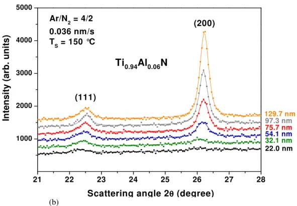
Fig. 1.20: Thickness dependent in-situ XRD spectra of Ti1-xAlxN samples deposited at different growth rates; (a) 0.092 nm/s, (b) 0.036 nm/s. A lower growth rate favours (100) preferred orientation[59]. ... 41
Fig. 1.21: Time-dependent in-situ specular X-ray reflectivity of fcc (Ti0.63Al0.37)N seed layers [(a) and (c)] and MAX phase Ti2AlN [(b) and (d)] on substrates MgO(111) [(a) and (b)] and MgO(100) [(c) and (d)]. The incidence and scattering angles were fixed at θ/2θ = 1.8° / 3.6° [(a) and (b)] and θ / 2θ=2.1° / 4.2° [(c) and (d)]. The oscillatory behaviour for the deposited seed layers as well as the Ti2AlN films on top are a fingerprint of layer-by-layer growth. The decreasing amplitudes of those oscillations reveal increasing roughness or island growth, which is more pronounced for the Ti2AlN film on MgO(100) (d) [93]. ... 44
... 48 Fig. 1.24: Grooves present in used sputtering targets; (a)Ni-Ti, (b) Ti, (c) Ni [101]. ... 49
Fig. 1.25: Photograph of a microwrapper fabricated using a Ni-Ti graded film [22]. ... 50 Fig. 1.26: RBS measurements; (a) initial 600 nm thick Ni-Ti layer deposited on the Si substrate,
(b) Ni-Ti layer deposited on the Ni-rich Ni-Ti layer (Y-axis: atomic composition of Ni and Ti, X
-axis: thickness of Ni-Ti layer) [22]. ... 50 Fig. 1.27: The crystallization temperature of the Ni-Ti films increases with Ar working pressure for
the same heating rate [115]. ... 53 Fig. 1.28: Comparison of activation energies: open symbols are data from Ni-Ti films and closed
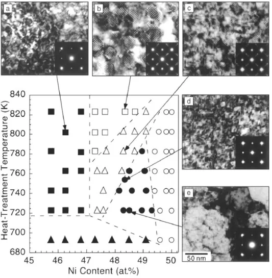
symbols from bulk Ni-Ti (K: Kissinger’s method, A: Avrami’s method, and X: X-ray method) [105]. ... 53 Fig. 1.29: DSC isothermal plots equiatomic Ni-Ti films (≈22 µm) released from a stainless steel
substrate showing broadening of crystallization peaks and an increase in incubation times as the crystallization temperature is lowered [116]. ... 54 Fig. 1.30: TEM micrograph of one of the two surfaces of a Ni-Ti film crystallized at 430°C and
quenched in liquid nitrogen after 25 min. It shows the microstructure resulting from surface nucleation of columnar grains (top) growing into remnant amorphous phase (bottom). The inset with a close-up of the interface reveals a grain size of approximately 1 µm [116]. ... 54 Fig. 1.31: Precipitation in the Ni-Ti matrix of Ti-rich Ni-Ti film (Ti-48.2at.%Ni) heat-treated for 1 h at various temperatures: ( ) are Ti2Ni particles with random orientation; ( ) are Ti2Ni precipitates
with the same orientation as that of the matrix; (∆) are plate precipitates and oriented Ti2Ni
precipitates; (•) are plate precipitates – d) high temperature form, e) low temperature form; (Ο) indicate no precipitates; ( ) indicate amorphous films [9]. ... 56
Fig. 1.32: GIXD patterns of Ni-Ti films during crystallization at an annealing temperature of 430ºC deposited on a Si(100) substrate at 70 mm – the indicated annealing time corresponds to the time when half a scan is completed [26]. ... 58 Fig. 1.33: Crystallized phase fraction versus crystallization time for Ni-Ti films deposited directly on
Si(100) wafers (h = 40 and 70 mm). The experimental data correspond to integrated peak
intensities of Ni-Ti B2(110) and (200), the theoretical values are obtained by using the Johnson-Mehl-Avrami equation [26]. ... 58 Fig. 1.34: Development of the B2(200) diffraction peak area during crystallization of the Ni-Ti films,
deposited on Si(100) with and without an intermediate poly-Si layer; (a) Ni-Ti deposited at 70 mm, (b) Ni-Ti deposited at 40 mm [26]. ... 59 Fig. 1.35: Schematic representation of oxidation of an equiatomic Ni-Ti alloy [125]. ... 62 Fig. 1.36: Multi-layered structure seen in cross-section of a specimen oxidized at 750°C [126]. ... 62 Fig. 1.37: Schematic diagrams of the microstructural evolution of interfacial reaction layers of
Ni-Ti/Si(100) annealed at 400-700°C for 30 min [130]. ... 65 Fig. 1.38: Cross-sections of crystallized Ti-50.0at%Ni films with different thicknesses and
strengthening mechanisms of films [136]. ... 67 Fig. 1.39: Residual stress and recovery stress for Ni-Ti films with different thicknesses [128]. ... 68 Fig. 1.40: Pole figures of Ni-Ti B2 phase nominally measured in the Bragg peaks B2(110) and
B2(200); (a) Ti-52.2at%Ni film which was crystallized at 700°C for 1 h, (b) Ti-51.6 at%Ni film heat-treated at 400°C for 1 h (the film was sputtered at 350°C) [23]. ... 72 Fig. 1.41: Transformation temperature of the films as a function of Hf content [150]. ... 74 Fig. 1.42: Room temperature XRD of Ni50Ti50-xHfx films after annealing at 550°C as a function of Hf
content [150]. ... 74
and the Si(111) crystals in the double-crystal monochromator. The maximum energy of 35 keV can be realized only with Si(311) monochromator crystals. Geometrical constraints of the DCM design limit the accessible energy range for Si(111) crystals to about 25 keV [152]. ... 79 Fig.2.4: Six-circle diffractometer in the MRH of ROBL; (a) view of the χ-circle (Eulerian cradle with inner diameter of 400 mm) with the x-y-z slide mounted directly on the azimuthal ϕ-circle (front
view: detector side), (b) scheme of the diffractometer with identification of the axes (view from back: beam direction). ... 81 Fig. 2.5: Deposition chamber mounted into the six-circle diffractometer of ROBL at ESRF (front
view-detector side); (a) “old” set-up, (b) “new” set-up. ... 82 Fig. 2.6: Sputtering chamber; (a) Perspective view, in the direction of the incident beam, of the sputter
deposition chamber for synchrotron X-ray scattering, (b) Cross-section with interior view of the sputter deposition chamber in a central plane [58]. ... 83 Fig. 2.7: Scheme of the accessible angles in off-plane scattering geometry; (a) “old” set-up [58], (b)
“new” set-up [156]. ... 85 Fig. 2.8: Atomic content of Ti in the Ni-Ti film versus DC sputtering power applied to the Ti
magnetron (with a constant power of 40 W applied to the Ni-Ti magnetron). ... 87 Fig. 2.9: Scattering angle 2θversus wavelength/energy. ... 88
Fig. 2.10: Diffractometer D-5000 (BRUKER AXS). ... 90 Fig. 2.11: Diffractometer D-5005 (BRUKER AXS) with an enlargement of the sample holder –
configuration for XRD measurements at T≥ RT. ... 91 Fig. 2.12: Diffractometer D-5005 BRUKER AXS with enlargement of the sample holder –
configuration for texture measurements. Picture taken during the determination of pole figures for a Ni-Ti film on MgO(100). ... 91 Fig. 2.13: (a) RBS equipment, (b) Geometry of the RBS experiment [158]. ... 92 Fig. 2.14: (a) AES spectrometer Microlab 310F (Fisons), (b) Aspect of a Ni-Ti sample after the AES
measurement (investigated spot indicated by the arrow)... 94 Fig. 2.15: (a) Transmission electron microscope CM300 SuperTWIN (Philips), (b) NiTi/SiO2/Si(100)
sample after removing the 2 pieces of 5×4 mm2 each for TEM preparation, (c) sample holder
(double tilt). ... 95
Fig. 2.16: Scanning electron microscope Hitachi S-4800 II. ... 96 Fig. 2.17: Four-probe experimental apparatus (van der Pauw geometry) used to measure the electrical
resistivity (ER) of the films (BIO-RAD HL 5550). ... 97 Fig. 2.18: Schematic of a rectangular van der Pauw configuration. ... 98 Fig. 3.1: XRD peak intensities during continuous co-sputtering of Ni-Ti for 143 min without Vb on a
naturally oxidized Si(100) substrate. Each scan corresponds to ≈ 2 min deposition; (a) in the diffraction range 17.0o<2θ<19.5o and (b) in the range 24.3o<2θ<26.8o (the z-axis scale represents
the detector intensity in cps). ... 101 Fig. 3.2: The net areas of the Bragg-Brentano B2(110) and B2(200) diffraction peaks and the lattice
parameter ao, as obtained from the positions of the respective peaks, recorded as a function of
time after start of Ni-Ti film growth on naturally oxidized Si(100); (a) deposited without
applying Vb, (b) deposited with a Vb of −25 V. ... 102 Fig. 3.3: Results obtained for the Ni-Ti sample deposited on naturally oxidized Si(100), with
Vb = −45 V, recorded as a function of time after start of film growth; (a) the net areas of the
Bragg-Brentano B2(110), B2(200) and B2(310) diffraction peaks, (b) ao as obtained from the
positions of the respective peaks. ... 103 Fig. 3.4: XRD spectra from a Ni-Ti sample deposited with a Vb of −45 V on naturally oxidized
Si(100), during annealing after deposition stop at 470°C and at RT. ... 104 Fig. 3.5: The net areas of the B2(110) and B2(200) diffraction peaks recorded as a function of time
after start of Ni-Ti film growth, as well as the values obtained for ao, on naturally oxidized
Si(111) without Vb. ... 105 Fig. 3.6: AES elemental concentration profiles for a Ni-Ti sample on naturally oxidized substrate
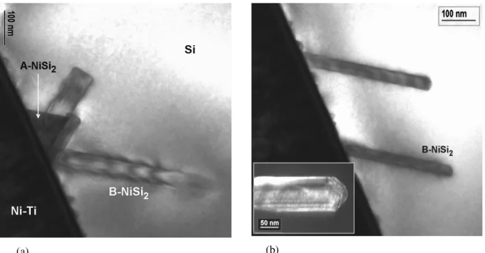
(a) two types of interfacial reaction products are perceptible in the image (A-NiSi2 and B-NiSi2),
(b) X-TEM micrographs focusing the presence of the B-NiSi2 in the Si(100) substrate. ... 107 Fig. 3.8: X-TEM micrographs of the interface’s morphology obtained on a sample grown on naturally
oxidized Si(100) without Vb. The main micrograph shows that A-NiSi2 grows epitaxially towards
the Si substrate with growth fronts {111} resulting in a semi-octahedron shape. The inset
represents the circled region in HR-TEM. ... 108 Fig. 3.9: X-TEM micrographs of a sample obtained on naturally oxidized Si(111) substrate
(without Vb); (a) overview of the Ni-Ti/Si(111) region, (b) HR-TEM enlargement of the
interfacial diffusion zone. ... 108 Fig. 3.10: X-TEM micrographs of a Ni-Ti/Si(111) sample deposited without Vb (recorded along the
Si[110] zone axis); (a) overview over the sample cross-section, (b) micrograph focusing the presence of the NiSi2 in the substrate (the angle between the line and the substrate surface is
roughly 70°). ... 109 Fig. 3.11: X-TEM micrographs of the Ni-Ti film grown without Vb on an intermediate layer of
poly-Si; (a) overall morphology, (b) micrograph with indication of the area (circle) studied in (c), (c) cross-section HR-TEM image showing Ni diffusion into the poly-Si layer. ... 110 Fig. 3.12: The net areas of the B2(110) and B2(200) diffraction peaks and the values obtained for ao,
represented as a function of time after start of Ni-Ti film growth on thermally oxidized Si(100) without Vb. ... 111 Fig. 3.13: In-situ XRD results for a Ni-Ti film deposited on thermally oxidized Si(100) with a Vb of
−45 V; (a) net areas of the B2(110) and B2(200) diffraction peaks recorded as a function of time, (b) ao values as obtained from the positions of B2(110) and B2(200) peaks as a function of time.
... 112 Fig. 3.14: XRD peak intensities during continuous co-sputtering of Ni-Ti for 128 min with a Vb of
−45 V on a thermally oxidized Si(100) substrate. Each scan corresponds to ≈ 3 min deposition: (a) in the diffraction range 17.0o<2θ<18.4o and (b) in the range 24.3o<2θ<26.8o. ... 113 Fig. 3.15: In-situ XRD results for Ni-Ti films deposited on thermally oxidized Si(100), without Vb,
deposited at ≈ 470°C and at ≈ 520°C; (a) net areas of the B2 diffraction peaks recorded as a function of time, (b) ao values as obtained from the positions of the B2 diffraction peaks as a
function of time. ... 114 Fig. 3.16: XRD spectra obtained at the deposition temperature (≈ 520°C) and at RT for a Ni-Ti sample deposited without Vb on thermally oxidized Si(100). ... 114 Fig. 3.17: AES elemental concentration profiles for the Ni-Ti sample on thermally oxidized Si(100)
substrate deposited without Vb. ... 115 Fig. 3.18: X-TEM micrographs of the Ni-Ti films grown on thermally oxidized Si(100) at ≈ 470°C;
(a) without Vb, (b) with a Vb of −45 V. A thin interfacial reaction layer is perceptible in both
cases. ... 116 Fig. 3.19: Bright field X-TEM micrographs of the films deposited on thermally oxidized Si substrates
at ≈ 470°C; (a) without Vb, (b) with a Vb of −45 V. ... 117 Fig. 3.20: X-TEM dark field image [Ni-Ti film deposited at ≈ 470°C on thermally oxidized Si(100)
without Vb] resulting from the selection of a spot associated with B2(100). The respective grains
show up as bright regions in the X-TEM micrograph. ... 117 Fig. 3.21: X-TEM micrograph showing the structure of the film from Fig. 3.20; (a) image obtained in
area 1 showing the B2(100) planes parallel to the interface, (b) indication of the interface
location. ... 118 Fig. 3.22: SAED pattern of the Ni-Ti film from Fig. 3.20 obtained in area 2 (surface region). ... 118 Fig. 3.23: TEM observations of the Ni-Ti film deposited at ≈ 470°C on thermally oxidized Si(100)
without Vb; (a) X-TEM micrograph, (b) SAED pattern obtained in area 3. B2(100) planes
parallel to the interface and B2(100) planes inclined by roughly 18° to the film surface are detected. ... 119 Fig. 3.24:Ex-situ XRD spectra with change of temperature (at RT and 100°C) using Cu-Kα radiation.
nominally measured in the Bragg peaks B2(110) and B2(200). The grey arrow indicates the direction of the vapour flux coming from the magnetron with the Ni-Ti target... 121 Fig. 3.26: Sections at ϕ = 0° and ϕ = 90° from the measured austenite pole figure of the 110
diffraction plane of the previous figure. ... 121 Fig. 3.27: Dependence of ER with temperature for three sample types (deposited at ≈ 470°C), during
(a) cooling and (b) heating. ... 123 Fig. 3.28: GIXD diffractograms (Cu-Kα radiation) at RT. The films had already been subjected to a
complete thermal cycle. ... 124 Fig. 3.29: (a)Net areas of the TiN(111) and TiN(200) diffraction peaks recorded during the
processing of a TiN buffer layer. (b) X-ray diffractograms from three TiN buffer layers ≈ 15, ≈ 80 and ≈ 215 nm thick. They were obtained in situ in vertical, i.e. off-plane Bragg–Brentano
scattering geometry immediately after the TiN deposition and before the deposition of Ni-Ti. In all cases a Vb of −30V was applied during TiN deposition. ... 126 Fig. 3.30: Typical XRR spectra; (a) for a 3 min deposition of a TiN buffer layer (black line) with the
fitting curve (red line), (b) obtained immediately after deposition (black line) and obtained 90 min after deposition of TiN (blue curve). A Vb of −30V was applied during the growth of the
TiN layers. ... 127 Fig. 3.31:In-situ XRD results for Ni-Ti films deposited without Vb on three different TiN buffer
layers; (a) net areas of the diffraction peaks of the B2 phase recorded as a function of time, (b) a0
values as obtained from the positions of the diffraction peaks as a function of time. ... 128 Fig. 3.32:The net areas of the B2(110) and B2(211) diffraction peaks, recorded as a function of time
after start of Ni-Ti deposition. The Ni-Ti film was deposited on a TiN layer (≈ 15 nm) previously deposited on top of a thermally oxidized Si(100) substrate; (a) without Vb, (b) with Vb = −45V.
... 129 Fig. 3.33:Lattice parameter ao, recorded as a function of time after start of Ni-Ti film growth on a TiN
layer (≈ 15 nm) previously deposited on top of a SiO2/Si(100) substrate. Results obtained for a
Ni-Ti film deposited without Vb and results obtained for a film deposited with Vb = −45 V are
represented. ... 129 Fig. 3.34: Effect of Vb applied during Ni-Ti deposition on TiN buffer layers of thickness ≈ 215 nm; (a)
the B2(110) net areas, (b) ao as calculated from the lattice constant, d, according to the B2(110)
peak position. ... 130 Fig. 3.35: XRD spectra obtained for the Ni-Ti films deposited without Vb, with −45 V and −90 V on
TiN buffer layers of thickness ≈ 215 nm; (a) after deposition at ≈ 470°C, (b) at RT. ... 131 Fig. 3.36: X-TEM micrographs from Ni-Ti samples deposited without Vb; (a) on a TiN layer of
thickness ≈ 15 nm, (b) on a TiN layer of thickness ≈ 215 nm. ... 132 Fig. 3.37: Ex-situ XRD spectra with change of temperature for the Ni-Ti samples obtained without
applying a Vb; (a), (b) at RT and (c), (d) at 100°C. ... 133 Fig. 3.38: Dependence of ER with temperature for the Ni-Ti samples (deposited without Vb) with TiN
buffers layers of thickness approximately 15, 80 and 215 nm during (a) cooling and (b) heating. ... 134 Fig. 3.39: Dependence of the ER with temperature for the Ni-Ti samples, deposited without and with a Vb of −45 V on a TiN buffer layer of thickness ≈ 15 nm; (a) during cooling and (b) heating. The
result from Fig. 3.38 has been inserted for comparison. ... 135 Fig. 3.40: Dependence of the ER with temperature for the Ni-Ti samples deposited without Vb, with
−45 and −90 V on a TiN buffer layer of thickness ≈ 215 nm; (a) during cooling and (b) during heating. ... 135 Fig. 3.41: AES elemental concentration profiles for the Ni-Ti samples on TiN buffer layers of
thickness ≈ 215 nm; (a) Ni-Ti deposited without Vb, (b) deposition using a Vb of −90 V. ... 136 Fig. 3.42: SEM micrographs showing the effect of the Vb on the surface morphology of Ni-Ti films
deposited on TiN buffer layers of thickness ≈ 215 nm. ... 137 Fig. 3.43: Time-dependent in-situ specular X-ray reflectivity for the first minutes of deposition of the
at ≈ 470°C on MgO(100) substrate (without Vb). ... 141 Fig. 3.45: Bragg-Brentano X-ray diffractograms obtained in situ during the deposition of a Ni-Ti film
at ≈ 470°C on MgO(111) substrate (without Vb). ... 141 Fig. 3.46:Time-dependent in-situ XRR for the TiN buffer layer and the first minutes of deposition of
the Ni-Ti film on MgO(100) substrate at ≈ 470°C. ... 143 Fig. 3.47:XRD results, for the Ni-Ti film deposited on TiN(100)/MgO(100), obtained during
deposition (without Vb). ... 143 Fig. 3.48: The net areas of the Bragg-Brentano B2(200) diffraction peak and the ao values as obtained
from the position of the peak, recorded as a function of time after start of Ni-Ti film growth on TiN(100)/MgO(100). ... 143 Fig. 3.49: XRD results, for Ni-Ti film deposited on TiN(100)/MgO(100), obtained at ≈ 470°C and RT.
... 143 Fig. 3.50: Pole figures of Ni-Ti B2 phase grown on MgO(100) substrate, nominally measured in the
diffraction peaks B2(110), B2(200) and B2(211). ... 144 Fig. 3.51: Atomic model illustration of the (100) crystallographic planes of; (a) Ni-Ti B2 phase, (b)
MgO. ... 145 Fig. 3.52: TEM observations of the Ni-Ti film attached to the MgO(100) substrate; (a) SAED pattern,
(b) dark field image taken in the reflection of MgO and (c) in the reflection of Ni-Ti,
respectively. ... 145 Fig. 3.53: Cross-section HR-TEM micrograph of the interfacial zone of the sample shown in Fig. 3.52. The lattice spacings of MgO(200) and Ni-Ti B2(110) planes are inserted in the micrograph. .. 146 Fig. 3.54: TEM observations of the Ni-Ti film attached to the MgO(100) substrate; (a) SAED pattern
of the overall sample, (b) dark-field image taken in the reflection selected in (a), (c) detail of an interfacial compound (dark-field) and (d) corresponding bright-field image. ... 147 Fig. 3.55: Dependence of the ER with temperature for the Ni-Ti sample on; (a) MgO(100) and (b)
MgO(111), during cooling and heating. ... 148 Fig. 3.56:In-situ XRD spectra of pure TiN film sputtered at low growth rate at 300°C. Ion irradiation
at a bias of −30 V leads to (100) preferred orientation in pure TiN. ... 149 Fig. 3.57:In-situ XRD results recorded as a function of time after start of TiN film growth on
thermally oxidized Si(100); (a) The net areas of the Bragg-Brentano 111 and 200 diffraction peaks of TiN, (b) comparison of in-plane lattice constants (a“111” and a200).and off-plane lattice constants (a111 and a200). ... 149 Fig. 3.58: XRR spectra with respective fits for the TiN film deposited on SiO2/Si(100) substrate. .. 150 Fig. 3.59: RBS analysis of pure TiN deposited on SiO2/Si(100) substrate showing data from
experiment and simulation. ... 150 Fig. 3.60: SEM micrograph of pure TiN deposited on SiO2/Si(100) substrate. ... 151 Fig. 3.61: Bright field X-TEM micrograph of the TiN film deposited on SiO2/Si(100) substrate at
≈ 300°C, with an enlargement of the topmost film’s region... 152 Fig. 3.62: XRD data of a growing film where for each 30 min the co-sputtering with Ti changed from
8 W to 20 W to 30 W to finally 0 W (deposition without Vb). 23 scans are added representing the
microstructural development of the Ni-Ti film (the zero intensities are manually inserted into the graphs to mark the various changes in the sputtering conditions; the z-axis scale represents the detector intensity in cps). ... 154
Fig. 3.63: In-situ XRD results for a Ni-Ti graded film deposited on naturally oxidized Si(100)
substrate during continuous co-sputtering of Ni-Ti (40W) and Ti (8/20/30/0W), during annealing and natural cooling. Represented are the net areas of the Bragg-Brentano B2(110), B2(200) and Ti2Ni(333/511) diffraction peaks as well as the a0 values as obtained from the
positions of the respective Bragg-Brentano peaks, as a function of time. ... 155 Fig. 3.64: AES elemental concentration profiles for the graded Ni-Ti film deposited on naturally
oxidized Si(100). ... 156 Fig. 3.65: X-TEM micrograph from the Ni-Ti graded film on the naturally oxidized Si substrate
delimitation of the spot associated with Ti2Ni(220), and the X-TEM dark field image resulting
from the selection of this spot. The respective Ti2Ni precipitates show up as bright regions in the
X-TEM micrograph... 158 Fig. 3.67:X-TEM micrograph showing the structure of the graded film near the interface
film/substrate. The B2(100) planes parallel to the interface were identified as well as the
presence of distinct phases at the interface. ... 158 Fig. 3.68: EDS results obtained using the line scan mode of the transmission electron microscope
along a distance of 430 nm, probing information from the substrate, interface and the Ni-Ti graded film. ... 159 Fig. 3.69: X-TEM micrograph of the interfacial zone of the Ni-Ti graded film with a black line
inserted on top of the thin Si oxide layer as a reference. Lattice spacings agreeing well with those of Ti2Ni were observed suggesting that the (111) planes of Ti2Ni make with the interface an
angle that leads the (400) planes approximately parallel to the interface. ... 160 Fig. 3.70: X-TEM micrograph (Ni-Ti graded film) focusing the presence of the B-NiSi2 in the Si(100)
substrate. ... 161 Fig. 3.71:Dependence of the ER in the Ni-Ti graded film with temperature during cooling and
heating. ... 162 Fig. 3.72: X-ray diffractograms obtained in situ during the deposition (Vb = −30V) of the TiN buffer
layer (deposition time = 40 min). ... 163 Fig. 3.73: Net areas of the B2(110), B2(200), B2(211) and Ti2Ni(333/511) diffraction peaks recorded
during the processing of the Ni-Ti graded film (Vb = −45V). ... 163 Fig. 3.74: Variation of the a0 values (as calculated from d according to the corresponding XRD peak
positions) during deposition, combined with the depth profile of the atomic concentrations in the Ni-Ti film (obtained ex situ). ... 164
Fig. 3.75: XRD spectra obtained at 470°C after the deposition process (top), and at RT (bottom). .. 164 Fig. 3.76: Dependence of ER with temperature during cooling and heating. ... 165 Fig. 3.77: SEM micrograph of the surface of the Ni-Ti film grown on the TiN buffer layer. ... 165 Fig. 3.78: RBS spectra of the NiTiHf films deposited ex situ on graphite substrates; (a) power applied
to the Ni-Ti magnetron: 40 W, (b) power applied to the Ni-Ti magnetron: 60 W. ... 166 Fig. 3.79: Overview of the composition results obtained for the NiTiHf films deposited ex situ after
the simulation of the data from Fig. 3.78 with the RUMP code. ... 167 Fig. 3.80: X-ray diffractograms obtained in situ during the deposition of a NiTiHf film at ≈ 470°C
(Ni-Ti = 60W and Hf = 13W) with Vb = −45 V. ... 168 Fig. 3.81: XRD spectra of the NiTiHf samples deposited at ROBL (Vb = −45 V); (a) obtained in-situ
after deposition, during the annealing period at ≈ 470°C, (b) at RT. ... 169 Fig. 3.82: XRD evaluation of phase transformation during cooling for the NiTiHf film from Fig. 3.80.
... 170 Fig. 4.1: Schematic unit cells of the B2 and B19’ phases of Ni-Ti alloy with the c axis chosen along
(110) in B2 and along (001) in B19’ (figure adapted from [137]). ... 193 Fig. 4.2: Model for the gradual change of the properties and possible precise tailoring, for a
two-dimensional bimorph Ni-Ti structure, resulting in a defined layering of austenite and martensite. ... 198 Fig. 5.1: Sputter deposition chamber inserted into the six-circles HUBER goniometer of ROBL
viewed from the detector side with the ion gun (gas supply connected) and the two magnetrons on top (left); design study from the beam entrance side (right) with symmetric magnetrons, ion gun, viewport between Be entrance windows, one turbo pump (70 l/s) at a corner valve which can be used for throttling and substrate alignment [156]... 204 Fig. 5.2: Bragg-Brentano X-ray diffractograms obtained in situ during the deposition of the Ni-Ti film
on a TiN buffer layer (total deposition time = 17.5 min) at ≈ 470°C. ... 205 Fig. 5.3: XRD scans in Bragg-Brentano geometry around the dominating B2(110) peak after the
Tab. 1.1: Factors affecting structure evolution in polycrystalline films [42]. ... 26 Tab. 1.2: Typical fibre textures observed in bcc metals and alloys (RD - rolling direction, ND -
normal direction). The α-fibre II is not common in general but is observed in SMAs [138]. ... 70
Tab. 2.1: Processing parameters used in the present study. ... 86 Tab. 2.2: Parameters used for the measurements at ROBL. ... 89 Tab. 3.1: Process conditions of near equiatomic Ni-Ti films deposited on naturally oxidized Si
substrate in the sputtering chamber of the beamline ROBL at ESRF. ... 101 Tab. 3.2: Process conditions of near equiatomic Ni-Ti films deposited on thermally oxidized Si(100)
substrate in the sputtering chamber of the beamline ROBL at ESRF. ... 111 Tab. 3.3: Process conditions of near equiatomic Ni-Ti films deposited on TiN buffer layers in the
sputtering chamber of the beamline ROBL at ESRF. The thickness of the Ni-Ti films was
≈ 800 nm (≈ 120 min of deposition). ... 125 Tab. 3.4: Process conditions of near equiatomic Ni-Ti films samples, on MgO single crystal
substrates, produced in the sputtering chamber of the beamline ROBL at ESRF. ... 139 Tab. 3.5: Process conditions of NiTiHf films produced in the sputtering chamber of the beamline
ROBL at ESRF during in-situ tests. ... 167
Tab. 5.1: Process conditions for the in-situ ion bombardment (using an ion gun) of a near equiatomic
INTRODUCTION
The combination of attractive properties like the shape-memory effect (SME), superelasticity (SE), high damping capacity, biocompatibility, high specific energy output, and excellent mechanical properties, as well as a very high resistance to corrosion has made Ni-Ti alloys one of the most technologically important Shape Memory Alloys (SMAs). The basic phenomenon enabling the SME and SE is related to the thermoelastic martensitic transformation. In the Ni-Ti system, while cooling, the high temperature phase (austenite - B2 structure, of the CsCl type) transforms into monoclinic B19’ martensite phase either directly or via intermediate rhombohedral R-phase transformation. The R-phase ⇔ B2 transformation is very useful for actuator applications because it is associated with a small temperature hysteresis, when compared to that of the B19’ ⇔ B2 transformation.
SMAs have been attracting attention as smart materials because they can work as sensors and actuators at the same time. Ni-Ti films are considered to be attractive candidates for micro-electro-mechanical system (MEMS) applications, since they can be patterned with standard lithography techniques and fabricated in batch processes. Furthermore, when compared with the bulk material, Ni-Ti films demonstrate fast cooling rates because of their higher surface/volume ratio, increasing substantially the heat transfer rate. Usually, Ni-Ti films are prepared using a sputtering method (on Si and on SiO2/Si wafers) although a number
of different fabrication methods are being tried. The composition and structure of the deposited films are significantly affected by the sputtering conditions (target power, gas pressure, target to substrate distance, deposition temperature, substrate bias voltage etc). Composition shifts can occur resulting from differences in sputtering yield, angular flux distribution, and lateral diffusion of the sputtered species because of atomic collisions with Ar and residual gases. A small deviation from stoichiometry can give rise to a significant precipitation of second phases. If the substrate is not heated during deposition, as-sputtered films are amorphous. These films need a post-deposition heat treatment in order to crystallize and be able to exhibit a thermally induced phase transformation.
between the intermediate layer of poly-Si and the crystallization behaviour, as well as the final structure of the deposited films, was discussed. It has been shown that the presence of a poly-Si buffer layer enhances the crystallization process of the Ni-Ti films, because of the higher number of nucleation sites provided by the rougher surface morphology of the poly-Si layer, when compared with a naturally oxidized Si(100) substrate. The in-situ studies of the structural development have been limited to post-deposition heat treatments and it seems essential to follow in situ the evolution of the structure of the growing film. Nowadays, despite several methods proposed for resolving some of the processing difficulties, the deposition of Ni-Ti films with definite stoichiometry and high purity remains a challenge. Moreover, it is clear from the published works that important issues like the formation of film texture and its control are still unresolved.
The aim of this PhD thesis is to study the optimisation of the deposition conditions for the formation of Ni-Ti films in order to obtain the material fully crystallized at the end of the deposition, and to establish a clear relationship between the substrates and texture development. In order to achieve this goal, a two-magnetron sputter deposition chamber has been used allowing to heat and to apply a bias voltage to the substrate. This equipment can be mounted into the six-circle diffractometer of the Rossendorf Beamline (ROBL) at the European Synchrotron Radiation Facility (ESRF), enabling an in-situ characterization by X-ray diffraction (XRD) of the films during their growth and annealing. In addition to the in-situ studies, complementary ex-situ characterization techniques such as XRD at a laboratory source, Rutherford backscattering spectroscopy (RBS), Auger electron spectroscopy (AES), cross-sectional transmission electron microscopy (X-TEM), scanning electron microscopy (SEM) and electrical resistivity (ER) measurements during temperature cycling have been used for a fine structural characterization.
The thesis consists of five principal chapters: (1) Background and literature review, (2) Experimental details, (3) Results, (4) Discussion and (5) Conclusions and future work.
between the substrates and texture development in the Ni-Ti films is highlighted, the essential points related with texture in films, like the different types of textures and the driving forces involved are described. This topic includes a review concerning texture development on TiN films due to the importance of the TiN layers for the present study. In the last section, several aspects regarding the production and characteristics of Ni-Ti films are discussed. Therefore, the importance of the composition control, the crystallization of the films and phenomena associated, the oxidation behaviour, as well as film/substrate interfacial reactions and the role of the thickness on the properties of the Ni-Ti films are presented. Further, a brief literature review related to texture in Ni-Ti materials (bulk and films) is also given. Finally, a short review about NiTiHf films is given to support the preliminary results obtained during the first tests of the deposition of this type of films at ROBL, with a view to explore the feasibility of the in-situ sputtering equipment for the future study of ternary alloys.
The equipment used to produce and to study in situ the evolution of the structure of the films during growth and annealing by synchrotron radiation scattering is discussed in chapter 2. The in-situ studies enabled to evaluate the structural evolution during deposition at fixed deposition parameters, as well as to identify the effect of changing parameters (Ti power target) on the structural characteristics of the film. A brief overview of the complementary ex-situ characterization techniques, such as XRD at a laboratory source, RBS, AES, X-TEM, SEM and ER measurements is also given.
The studies have focused on the following points:
• deposition of Ni-Ti films on different types of substrates, such as naturally and thermally oxidized Si(100) substrates and MgO single crystal substrates;
• analysis of the role of a TiN buffer layer on the growth of the Ni-Ti film; • influence of the bias voltage applied to the substrate during Ni-Ti growth;
• the characterization of graded films (controlled change of the Ti:Ni ratio during deposition).
For each situation, special attention is paid to the stability of the preferential orientation of the austenitic phase during the deposition process, trying to answer the question of how and when the different textures generate.
the Ti:Ni ratio during the deposition of Ni-Ti films are presented (the first reported studies on the topic). During the in-situ study, the evolution of the intermediate structural “states” of the growing film has been identified, which cannot be seen/revealed ex-situ, because those states occurred only during the growth but were no longer detectable after deposition.
Chapter 4 discusses the preferential orientation of the films, the interface analysis and their link with the phase transformation characteristics.
1. BACKGROUND AND LITERATURE REVIEW
In the first section of this chapter, an overview of the Ni-Ti alloy system is given in relevance to the discussions on the composition control, the phases present in the films and phase transformation. The Shape Memory Effect (SME) and Superelasticity Effect (SE) are also explained.
The second section of this chapter is dedicated to the phenomena involving the deposition by sputtering of thin films in general. A short introduction to the sputtering process, which includes the growth and morphology of the films, is given. The ion bombardment effects and various considerations about stress in the films are also presented. It is as well described important points related to texture in films like the types of textures and the driving forces involved. TiN sputtered films are frequently mentioned in this section due to their importance for the present study.
In the last section of chapter 1, several aspects concerning the production and characteristics of Ni-Ti films are reviewed. Hence, the importance of the composition control, the crystallization of the films and related phenomena, the oxidation behaviour, as well as the interfacial film/substrate reactions and the role of the thickness on the properties of the Ni-Ti films are discussed. A brief review of texture in Ni-Ti SMA materials (bulk and films) is also given, as it assumes an important role. At the end, a short review about NiTiHf films is given to support the preliminary results obtained during the first tests regarding the deposition of ternary SMA alloys at ROBL.
1.1. Ni-Ti SHAPE MEMORY ALLOY
Ni-Ti alloys became one of the most technologically important SMAs due to the excellent combination of attractive properties like the SME, SE, high damping capacity, biocompatibility, high specific energy output and excellent mechanical properties, as well as a very high resistance to corrosion [1]. The thermoelastic martensitic transformation enables the SME and SE.
the monoclinic martensitic phase has been a subject of study for several researchers [3-8]. It can be observed if the alloy is subject to specific processing conditions like: variation of Ni content, introduction of a ternary element, thermal annealing, thermal cycling or cold working. The R-phase ⇔ B2 transformation is associated with a small temperature hysteresis, when compared to that of the B19’ ⇔ B2 transformation. The R-phase presents other attractive features like stability against thermal cycling and negligible strain-recovery fatigue, although the associated strain is smaller (0.5 %-1 % instead of 6.5 %-8.5 % of that of the later).
The capability to transmit particularly high forces along with a large stroke make SMAs a material with the greatest specific work output of several actuation mechanisms (Fig. 1.1) [9]. For comparison, bulk piezoelectric materials produce a large force over extremely small displacements, while piezo-bimorphs have large displacements but produce small forces.
Fig. 1.1: Power/weight ratio versus weight for SMA actuators as compared with other devices,
demonstrating the relatively large output of SMA actuators given their small size [9].
1.1.1. Phase diagram and crystal structures
The Ni-Ti alloy system is very attractive, since the alloy can be improved by utilizing various phase transformations, both diffusional and diffusionless. The SME and SE occur in near equiatomic Ni-Ti alloys with compositions ranging from ≈ 45-55 at.% Ni.Observing the Ni-Ti binary phase diagram in Fig. 1.2 [1], it is visible that the solubility in Ni-Ti changes gradually with temperature on the Ni-rich side, while it has a steep solvus boundary on the Ti-rich side. A small deviation from stoichiometry in Ni-Ti alloys can give rise to a significant precipitation of second phases. It was found that in Ni-rich Ni-Ti alloys, diffusional transformations take place during aging or slow cooling from high temperature. The precipitation sequence can be written as B2 Ni4Ti3 Ni3Ti2 Ni3Ti (stable) [11]. The Ni4Ti3
metastable phase (rhombohedral until cell) appears at lower temperatures and at shorter aging times. The presence of Ni4Ti3 is especially important for improving shape-memory
characteristics and strength, since it precipitates on a very fine scale. The inset of Fig. 1.2 shows the metastable equilibrium between Ni-Ti and Ni4Ti3.
Nishida et al. [11] have studied the precipitation processes in Ni-rich Ni-Ti alloys and reported the TTT (time-temperature-transformation) diagrams for several composition alloys. At lower aging temperature and shorter aging time, Ni4Ti3 phase appears, while at higher
aging temperature and longer aging time Ni3Ti phase appears and at intermediate temperature
and time Ni3Ti2 phase appears (Fig. 1.3). Further studies [12] were conducted in an aged
Ti-52 at% Ni alloy in order to clarify details of the microstructural aspects of the Ni3Ti2 phase
using optical and electron microscopy and electron diffraction. It has been found that the Ni3Ti2 precipitate exhibits a phase transformation. The sequence of transformation events was
described as occurring in two-step transformations: parent phase (tetragonal) ⇔ intermediate phase (orthorhombic) characterized by antiphase-like domain morphology ⇔ low temperature phase characterized by antiphase and needle-like domains morphology (monoclinic). Later, Hara et al. [13] have performed a study to determine the crystal structure of the Ni3Ti2
precipitate and to clarify the characteristics of the transformation from the crystallographic point of view. The crystal structure of the high and low temperature phases, and twinning in the low-temperature phase were studied in detail. The crystal structure of the high-temperature phase is tetragonal with Pd3Ti2 type (space group: I4/mmm). The values
determined by the Rietveld method for the lattice parameters were: a = 0.3095(38) and c = 1.3585(169) nm. The low-temperature phase exhibits an orthorhombic structure with Al3Os2 type (Bbmm). The lattice parameters obtained were: a = 0.4398(49), b = 0.4370(48),
and c = 1.3544(150) nm.
Commercially used Ni-Ti alloys frequently contain a small volume fraction of intermetallic precipitate phase, normally Ni4Ti3 or Ti2Ni, distributed in the B2 matrix. It is
known that these phases can produce coherency strains and affect the transformation and mechanical characteristics of the alloy. However, in the Ti-rich side the solubility limit is almost vertical and the manipulation of the Ti2Ni precipitates cannot be easily employed to
improve the properties of the alloy. This situation changes in crystallized films via amorphous state, which is a non-equilibrium state, and even microstructures quite different from those of bulk materials can appear. This subject will be discussed in more detail in section 1.3.2.
The martensitic transformation in Ni-Ti SMA is a first order phase transformation that does not require long-range atomic migration to form the new crystal structure. When the high temperature B2 austenite phase is undercooled to a certain temperature (martensite start), it becomes unstable and transforms to a lower symmetry martensite (B19’) by a shear-dominated, cooperative movement of atoms.
The parent phase of equiatomic Ni-Ti is a CsCl-type B2 cubic structure with a lattice constant of 0.3015 nm and the space group is Pm3 m. The crystal structure is shown in Fig. 1.4(a). The low-temperature phase which can form with the same composition as the parent phase with a diffusionless transition has a monoclinic structure (AuCd type), denoted B19', as shown in Fig. 1.4(b) [14]. It belongs to space group P21/m. Kudoh et al. [15] found
the following lattice parameters for the martensite phase: a = 0.2898 nm, b = 0.4108 nm, c = 0.4646 nm, and β = 97.78° (Ti-49.2at% Ni alloy tested at 50°C).
(a) (b)
Fig. 1.4: (a) B2 austenite phase, (b) B19’ martensite phase [14].
observed by electron microscopy) [16]. R-phase was reported as a rhombohedral distortion and the lattice can be described by stretching the cubic parent lattice along the <111> diagonal direction. If we define the corner angle α, which is 90° in B2 parent phase, as shown in Fig. 1.5, it deviates from 90° with changing temperature.
Cubic (B2) austenite phase Rhombohedral (R) phase Fig. 1.5: Transformation of cubic (B2) austenite to rhombohedral (R) phase [17].
The SME and the SE are linked with the thermoelastic transformation. One of the most important characteristics of SMAs is the temperature at which it changes from one crystalline structure to the other. The characteristic temperatures of a phase transformation will be referred as follows:
• Ms : martensite-start temperature (upon cooling);
• Mf : martensite-finish temperature (upon cooling);
• As : austenite-start temperature (upon heating);
• Af : austenite-finish temperature (temperature at which
martensite becomes completely unstable upon heating);
• Rs : R-phase-start temperature on cooling;
• Rf : R-phase-finish temperature on cooling;
• R’s : R-phase-start temperature on heating;
• R’f : R-phase-finish temperature on heating.
composition can change the transformation temperatures by more than 100°C. In the Ni-Ti system, the Ni-rich side has some solubility at high temperature (Fig. 1.2) and the transformation temperatures are strongly dependent on the Ni concentration. Increasing Ni causes a drastic decrease in the transformation temperatures. The martensitic transformation temperature drops to below 100 K for a Ni content exceeding 51.5 at.% (Fig. 1.6). On the Ti-rich side the transformation temperatures do not exhibit such dependence with composition, probably due to the fact that the solubility limit of Ni-Ti phase on the Ti-rich side is almost vertical.
Fig. 1.6: Ms as a function of Ni content for binary Ni-Ti SMA. The different symbols represent data from different authors and the solid line is given by thermodynamic calculations [18].
The phase transformations can be investigated by measuring some physical properties such as electrical resistivity (ER) as a function of temperature. This technique was chosen in order to study the Ni-Ti films produced during this PhD work. Figure 1.7 shows the temperature dependence of the resistivity for a Ni-Ti bulk sample heat-treated at 380°C, obtained by Uchil et al. [19]. During cooling from B2-phase, the resistivity value decreases linearly with the temperature down to Rs. Self-accommodated R-phase transformation starts at
Rs and the austenite parent phase (B2) transforms to the twinned R-phase with further
decrease of the temperature. Twinning in an alloy matrix results in electron scattering that in turn leads to the increase of the ER [17]. The twinned structure density in B2 phase increases with the decrease of the temperature (due to the B2 R-phase transformation), producing a higher ER as a result of the more pronounced increase of lattice imperfections. R-phase transformation ends once the temperature decreases to Rf. An additional cooling promotes the
which exhibits less lattice distortion. The martensite transformation finishes when the temperature reaches Mf, and, cooling below Mf, does not result in more phase changes. On
heating, the authors did not identify the R-phase reverse transformation. The transformation to cubic B2 austenite parent phase is completed at temperature Af and the microstructure
completely reverses to the original microstructure consisting of single cubic B2 austenite.
Fig. 1.7: Temperature dependence of electrical resistivity of a Ni-Ti sample, heat-treated at 380°C, in a complete thermal cycle [19].
1.1.2. Shape memory effect (SME) and superelasticity effect (SE)
The SME in Ni-Ti alloy was discovered in the 1960s at the Naval Ordnance Laboratory [20], hence the acronym Nitinol is commonly used in referring to the Ni-Ti system (Nickel Titanium Naval Ordnance Laboratory). The SME is a result of the change in crystalline structure as the material is heated and cooled. The martensitic transformation is a displacive type solid-state transformation and atoms are cooperatively rearranged or shifted into a new structure (without diffusion). The displacement of each atom is not large but since all of the atoms move in the same direction in a domain or variant, the transformation results in a macroscopic change in shape. This phenomenon may lead to unique properties such as the SME and SE. The martensitic transformation is described by a shear-like mechanism, as shown schematically in Fig. 1.8(a) and (b) [1]. When the B2 parent phase in Fig. 1.8(a) is cooled below Ms, the structure changes into martensite, as in Fig. 1.8(b). The formation of
![Fig. 1.7: Temperature dependence of electrical resistivity of a Ni-Ti sample, heat-treated at 380°C, in a complete thermal cycle [19]](https://thumb-eu.123doks.com/thumbv2/123dok_br/16686758.743446/35.892.236.656.263.552/temperature-dependence-electrical-resistivity-sample-treated-complete-thermal.webp)
![Fig. 1.18: Pole figures; (a) Permalloy (Ni 80 Fe 20 ) film exhibiting a strong <111> fibre texture [64], (b) (200) pole figure for a MgO film (without substrate rotation - the direction of the vapour flux](https://thumb-eu.123doks.com/thumbv2/123dok_br/16686758.743446/57.892.110.801.709.975/figures-permalloy-exhibiting-strong-texture-substrate-rotation-direction.webp)
![Fig. 1.21: Time-dependent in-situ specular X-ray reflectivity of fcc (Ti 0.63 Al 0.37 )N seed layers [(a) and (c)] and MAX phase Ti 2 AlN [(b) and (d)] on substrates MgO(111) [(a) and (b)] and MgO(100) [(c) and (d)]](https://thumb-eu.123doks.com/thumbv2/123dok_br/16686758.743446/65.892.159.748.101.526/fig-time-dependent-specular-reflectivity-layers-phase-substrates.webp)
![Fig. 1.22: Ratio of the optical emission intensity of Ni to Ti versus the product of pressure and distance target/substrate [111]](https://thumb-eu.123doks.com/thumbv2/123dok_br/16686758.743446/68.892.262.626.251.570/ratio-optical-emission-intensity-product-pressure-distance-substrate.webp)
![Fig. 1.38: Cross-sections of crystallized Ti-50.0at%Ni films with different thicknesses and strengthening mechanisms of films [136]](https://thumb-eu.123doks.com/thumbv2/123dok_br/16686758.743446/88.892.292.620.481.877/cross-sections-crystallized-films-different-thicknesses-strengthening-mechanisms.webp)
![Fig. 1.39: Residual stress and recovery stress for Ni-Ti films with different thicknesses [128]](https://thumb-eu.123doks.com/thumbv2/123dok_br/16686758.743446/89.892.244.658.692.1106/fig-residual-stress-recovery-stress-films-different-thicknesses.webp)