Ruben Miguel Seixas Aguincha
Licenciatura em Ciências de Engenharia FísicaCarbon Based Surfaces with Low Secondary
Electron Emission
Dissertação para obtenção do Grau de Mestre em Engenharia Física
Orientador:
Nenad Bundaleski, Investigador, FCT-UNL
Co-orientador:
Orlando Teodoro, Professor Associado, FCT-UNL
Júri:
Carbon Based Surfaces with Low Secondary Electron Emission
Copyright cRuben Miguel Seixas Aguincha, Faculdade de Ciências e Tecnologia,
Univer-sidade Nova de Lisboa
A
CKNOWLEDGEMENTS
First of all I would like to thank to Faculdade de Ciências e Tecnologia of Universidade Nova de Lisboa (FCT-UNL) for being the great school it is, where I could learn, make friends and have unforgettable moments throughout these years.
I would also like to thank to the following people:
Nenad, for the first of many bus rides, where the idea for this same work came up; For the entire support, good mood, patience and being the greatest teacher in these past months.
Professor Orlando, for agreeing to be my co-supervisor and for all the patience and teachings, not only in these past few months but throughout the entire course.
Ana and Afonso, for all the support, ideas, help and good will.
Paulo Duarte from REQUIMTE, for the help in my introduction to electrochemistry.
The research team of Plasma Engineering Laboratory at Institute of Plasma and Nul-cear Fusion of IST and particularly Neli Bundaleska, for providing graphene/N-graphene samples produced in the framework of PEGASUS (H2020 FETOPEN 766894) project. Without it, my entire work wouldn’t be possible.
All my family and friends, for the incredible patience, support and everlasting friend-ship.
My parents, for their greatest effort so I could get to this very moment.
My "fatty" sis for being the greatest sister, friend and role model I could ever ask for.
A
BSTRACT
Low secondary electron emission materials have significant impact in accelerator and space technologies. Secondary electrons produced by the residual gas ionization or due to the irradiation of chamber walls by the synchrotron light influence trajectories of charged particles inside accelerators. Significant potential difference between the dielectric and conductive parts of satellites is caused by different secondary electron emission yields in-duced by cosmic rays, leading to discharges between different parts of a satellite, resulting in the malfunctioning of the communication systems and other sensitive equipment. One of the solutions to these problems is coating surfaces with thin films of amorphous carbon. Recent studies showed that graphene-based coatings have a potential in further reduc-tion of secondary electron yields (SEY). For that reason, the deposireduc-tion of free standing graphene (i.e. graphene in the form of powder) on technical surfaces of interest in space and accelerator technologies using Electrophoretic Deposition (EPD) was investigated in this work. Highly oriented pyrolytic graphite and pure graphene samples were used as references in order to compare them with graphene coatings produced by EPD. Apart from SEY measurements, X-ray photoelectron spectroscopy and scanning electron microscopy of the samples were performed for that purpose. Graphene depositions were successfully made and the maximum SEY of technical surfaces (stainless steel and copper) was reduced to∼1. In order to achieve these results, various studies were performed concerning the
deposition technique parameters, related to the process and the materials used. Three different alternatives were also explored.
R
ESUMO
Materiais com baixa emissão secundária de electrões têm um grande impacto na tec-nologia espacial e de aceleradores de partículas. A trajectória das partículas carregadas no interior dos aceleradores é influenciada por electrões secundários produzidos pela ionização de gás residual ou pela irradiação das paredes das câmaras por radiação de sincrotrão. Nos satélites de comunicações, a radiação cósmica origina diferentes taxas de emissão de electrões secundários em materiais condutores e dielétricos constituintes do equipamento. Este efeito origina grandes diferenças de potencial entre estes materiais, consequentemente levando à avaria e mau funcionamento dos sistemas de comunicações e outros equipamentos sensíveis. Uma das soluções para estes problemas é revestir as superfícies com filmes finos de carbono amorfo. Estudos recentes demonstram que re-vestimentos à base de grafeno têm um grande potencial na redução da taxa de emissão de electrões secundários (SEY). Por esta razão, foi estudada neste trabalho a deposição electroforética (EPD) de grafeno em forma de pó em superfícies técnicas no interesse da tecnologia espacial e de aceleradores de partículas. Grafite pirolítica altamente orientada e grafeno puro (na forma de pó) foram usados como referências com o objectivo de poderem ser comparadas às deposições de grafeno produzidas por EPD. Além de medições de SEY, XPS e SEM foram também usadas para analisar e caracterizar as amostras produzidas. As deposições de grafeno foram realizadas com sucesso e foi ainda possível diminuir o SEY das superfícies técnicas usadas (aço inoxidável e cobre) para∼1. Para atingir os
resultados obtidos, foram realizados vários estudos relativamente aos parâmetros do processo de deposição e aos materiais usados na mesma. Foram ainda exploradas três diferentes alternativas a este processo.
Palavras-chave: Aceleradores de partículas, satélites de comunicações, SEY, Grafeno,
C
ONTENTS
List of Figures xv
List of Tables xvii
1 Introduction 1
1.1 State of the Art. . . 2
2 Concepts and Experimental Techniques 5 2.1 Fundamental Concepts . . . 5
2.1.1 Secondary Electron Emission - SEE . . . 5
2.1.2 Secondary Electron Yield - SEY . . . 6
2.1.3 Graphene . . . 10
2.2 Experimental Techniques. . . 13
2.2.1 Electrophoretic Deposition - EPD . . . 13
2.2.2 SEY apparatus . . . 18
2.2.3 X-Ray Photoelectron Spectroscopy . . . 22
2.2.4 Scanning Electron Microscopy . . . 27
3 Experimental Procedures 31 3.1 EPD procedure . . . 31
3.2 SEY measurement procedure . . . 33
4 Results and Discussion 35 4.1 Substrates’ analysis . . . 38
4.2 Choice of the counter electrode . . . 40
4.3 Tuning the deposition parameters . . . 43
4.4 SEY results of samples obtained with optimized deposition parameters . . 49
4.5 Ageing of electrodes . . . 53
4.6 Alternative 1 - CVD grown graphene . . . 55
4.7 Alternative 2 - Graphite coating by EPD . . . 58
4.8 Alternative 3 - Graphite spray . . . 60
CONTENTS
L
IST OF
F
IGURES
2.1 Three steps for the productions of true secondary electrons [4].. . . 6
2.2 Illustration of a typical SEY curve as a function of primary electron energy [16]. 8 2.3 Correlation between the angle of incidence of primary electrons and their depth. 9 2.4 Examples for SEE on grooved surfaces [13]. . . 9
2.5 Hexagonal lattice of graphene. . . 10
2.6 sp3hybridization tetrahedron shape [18]. . . 11
2.7 Trigonal planar geometry ofsp2hybridization [19]. . . 12
2.8 Scheme of standard CVD grown graphene [20].. . . 12
2.9 Process scheme of microwave atmospheric plasma based production of free standing graphene [22]. . . 13
2.10 Schematic of EPD phenomena [23]. . . 14
2.11 Diagram of double layer and zeta potential of a particle in an ionic fluid [25]. 14 2.12 Simulation of the electric field around the electrode [23]. . . 15
2.13 Home-made apparatus for EPD. . . 18
2.14 Measuring method of primary and secondary currents [4]. . . 19
2.15 Instrumentation layout of the homemade apparatus for SEY measurement [4]. 20 2.16 Illustration of SEY measuring errors. . . 21
2.17 Schematic of photoemission process and Auger effect. . . 22
2.18 Instrumentation layout of a typical XPS instrument [30]. . . 24
2.19 Multiplet structure associated with the Cr 2p3/2peak for a vacuum fractured Cr2O3specimen [35]. . . 26
2.20 Mechanisms of secondary electrons emission, backscattered electrons, and characteristic X-rays from SEM’s samples [37]. . . 28
2.21 General schematic of a SEM’s instrumentation [38]. . . 29
3.1 EPD procedure diagram. . . 32
3.2 SEY measurement procedure diagram. . . 33
3.3 Typical results of a SEY measurement. . . 34
4.1 SEM image of free standing graphene sheets produced in IST [22].. . . 36
4.2 Carbon 1s line of HOPG and free standing graphene. . . 37
4.3 SEY curves of HOPG, graphene and N-doped graphene. . . 38
LIST OFFIGURES
4.5 Cu 2p3/2 line fitting. . . 39
4.6 Cr 2p3/2and Fe 2p3/2lines fitting. . . 40
4.7 Carbon 1s line using Au and SS as counter electrodes. . . 41
4.8 SEY curves for Au and SS as counter electrodes. . . 42
4.9 Oxygen 1s line of the 15 and 90 minutes. . . 43
4.10 SEM image of 90 minutes sample from which the thickness was estimated.. . 44
4.11 SEY curves as function of time of deposition. . . 45
4.12 SEY curves as function of voltage of deposition. . . 47
4.13 SEM images for 40 V deposition sample. . . 47
4.14 SEM images of the sample produced with HCl in excess. . . 48
4.15 EDS measurement of gold nanoparticles present in figure 4.14(b). . . 49
4.16 Cu 2p3/2 fitting of the CuAu sample. . . 49
4.17 SEY curves of the three lowest SEY samples. . . 51
4.18 SEM images of SSAu, CuAu and CuSS samples. . . 51
4.19 Picture of pitting effect on stainless steel electrode. . . 53
4.20 SEM images of the Au electrode after EPD of graphene and graphite. . . 54
4.21 SEY curves for CVD grown graphene coatings. . . 56
4.22 Carbon 1s line of CVD grown graphene samples. . . 57
4.23 Optical microscope images of CVD graphene coated samples. . . 58
4.24 SEY curves of bare SS, graphite and graphene by EPD. . . 59
4.25 SEM images of graphite coating by EPD.. . . 60
4.26 SEY curves of bare SS, Graphit 33 and graphene reference sample. . . 61
L
IST OF
T
ABLES
2.1 Main differences between EPD and Electroplating [26]. . . 16
2.2 Correlation between the degenerate states and respective intensity ratios. . . 23
4.1 Peak position of O contributions in C 1s line fitting [43]. . . 36
4.2 Surface composition of used substrates. . . 38
4.3 Composition analysis of the material deposited on SS using Au and SS as counter electrodes. . . 41
4.4 sp2andsp3ratio using Au and SS electrodes. HC stands for hydrocarbon and different C-O bonds. . . 41
4.5 sp2andsp3ratio according to deposition time. . . 44
4.6 Table of elemental composition for different deposition voltages. . . 45
4.7 C 1s fitting for different deposition voltages. . . 46
4.8 Cr 2p3/2 fitting for different deposition voltages. . . 46
4.9 Composition table of the three samples with the lowest SEY. . . 50
4.10 Surface composition of SSAu, CuAu and CuSS* relative to before baking mea-surements. . . 53
4.11 Surface composition of Au electrode before and after EPD. . . 54
4.12 Composition analysis of CVD grown graphene samples. . . 55
4.13 C 1s line contributions of CVD graphene samples. . . 57
C
H
A
P
T
E
R
1
I
NTRODUCTION
Development of low Secondary Electron Yield (SEY) materials is very important in dif-ferent modern technologies, spanning from space applications, via modern accelerators, to the vacuum gauges. Altering the surface composition with coatings of amorphous carbon to reduce SEY has been studied for years. This resulted in recent coating of several kilometers of tubes by this material in Super Proton Synchrotron in CERN, which is the accelerating device preceding Large Hadron Collider [1]. Recent investigations have shown that this could be further improved with graphene coatings [2]. Since graphene is a form of graphitic carbon it has low secondary electron emission and its unusual properties let us suppress the SEY even further [3]. It is important to point out that not every kind of carbon has low SEY, only the conductive ones. Graphene, the first 2D material discovered by Geim and Novoselov in 2004, is conductive carbon material with numerous interesting properties including low SEY. Graphene can be produced by a great variety of methods but each of them will result in different types of graphene, concerning its defects and impurities, which will influence its secondary emission properties.
The main goal of this project will be to study SEY from carbon coatings, and correlate the surface characteristics (composition, morphology and electronic structure) with the secondary electron emission properties. It will be used an electrochemical technique (Electrophoretic Deposition - EPD) to produce different coatings, and to further study the influence of substrates and different deposition parameters. The composition of surfaces will be characterized by XPS and its morphology by SEM, while the SEY will be measured on the existing home-made apparatus [4].
CHAPTER 1. INTRODUCTION
1.1
State of the Art
Secondary electron emission (SEE) has always been a problem in particle accelerators and in space technologies, namely, communications satellites. The problem known as electron cloud (e-cloud) was discovered by Soviet accelerator scientists from Novosibirsk the middle 60-ies. But, at that time, it was of minor significance with respect to other problems related to the beam stability. With the advancement of the accelerator technologies e-cloud effect became the major limitation of modern accelerators and synchrotrons.
Everything begins with the ionisation of the residual gas. As a result of that, one energetic electron is kicked out from the atom/molecule hitting the tube wall and may initiate electron multiplication. Electron cloud is formed, which will live for some time before being absorbed. In accelerators, ions travel in the form of bunches (pulses). If an electron cloud survives until the next bunch come to the same spot, negative charges will bend the beam and introduce the instability. If the objective is to increase the number of collisions in the accelerator, the number of bunches per second needs to be increased (i.e. decrease the time between bunches). For that reason, the lifetime of an e-cloud must be reduced.
Low energy electrons have low SEY because the probability to originate secondary electrons is also low, but for electrons at energies and angles with secondary electron yield above 1, the number of secondary electrons grows exponentially [5]. These electrons will interfere with the primary beam which may influence its trajectory and cause beam instabilities.
Concerning telecommunication satellites, SEE influences the maximum power han-dling capabilities of the satellite waveguide components. The Multipactor effect is an electron cloud in devices working in vacuum, where the exponential electron multiplica-tion by SEE from the walls in resonance with the radio frequency field, distorts the signal and eventually evolves into discharge between the dielectric and conductor materials damaging and even destroying the communications devices [6].
Nowadays there are three main solutions to this subject [7]:
1. Changing the surface composition;
2. Modifying the surface morphology;
3. The “Dose” effect.
1.1. STATE OF THE ART
to be employed.
Changing the surface composition has been the solution under numerous investiga-tions, since it is the most suited method concerning its application in this area of interest. Ideally clean metals are much better for this purpose but they lead to other problems, namely, the oxidation of their surface which alters completely their properties. So, this method consists in applying a thin film of another material on a certain surface. This material must have very good SEE properties which leads to low SEY, and they must be chemically inert, so the properties of the film material are one of the main concerns of this method. Throughout the years there has been various studied materials which led to a reduction of the SEY, such as TiN, TiC, NbC and NbN. Titanium Nitride (TiN) films are known to reduce SEY [8] depending on the deposition method. From various studies there is a large variation of results concerning maximum SEY measurements, but the best layers of TiN are known to have maximum SEY values (1.6 - 1.7) lower than any known as-received metals (2.5 - 3) [9][7]. All other materials have revealed very similar results for the minimization of the multipacting effect although their exposure to air resulted in an increasing of the SEY (∼0.4 for TiN) [10]. It is essential to preserve low SEY after air
exposure and after baking, since these are potential walls of UHV chambers, which will be opened or baked, from time to time. In that respect, TiN would not be a suitable choice.
In the last few years, coatings of amorphous carbon, graphite and more recently graphene, have been frequently studied because of their SEE properties. Amorphous carbon and graphite are two forms of carbon with the lowest known SEY’s in the lit-erature (1 - 1.5) [11]. Amorphous carbon is a reactive allotrope of carbon that does not have a crystalline structure and is usually stabilized with hydrogen bonds in terminating freeπbonds. Carbon coatings prepared by magnetron sputtering can reach a maximum
SEY close to 1 with a deviation that can go from 0.8 to 1.15 depending on their aging process (increasing the amount of hydrogen due to air exposure) [11]. Graphene is a very special material due to its unique electronic, optical, mechanical and thermal prop-erties. Studies have showed that a mono/double layer of graphene on a flat substrate in vacuum has ultralow SEY, of the order of 0.5 [6]. The graphene can be synthesized by a variety of methods and in some cases, it can be grown directly on the substrate (Au, Ag, Cu and Si) which make it even easier to be used as a low SEY material. It was shown in different studies that graphene coatings, chemically made from graphite, can reduce the SEY of the surface at least 50% with the thickness of the film in a nano-scale [12].
CHAPTER 1. INTRODUCTION
of future generations secondaries is low enough that they are absorbed by the surface [13]. The corrugations can be produced by electrochemical reactions directly with the substrate (so called chemical etching) or by the deposition of strongly roughened layer. This method was first tested in a copper substrate [7], where it was grown an oxide layer at high temperatures and the stress generated by the sudden temperature change, led to the opening of cracks in the oxide layer which created specific surface morphology [7]. This oxide layer (as any metallic oxide) has a relatively high SEY, so when combined with surface roughness it can be clearly seen a suppression in SEE. Altering the surface morphology is an efficient way to reduce the SEY but it’s a difficult method to apply to a larger scale.
A combination of the first and second methods can also be possible when it is used amorphous carbon or free-standing graphene coatings [6] where the SEE properties of the material are extremely good but its roughness decreases even more the SEY.
C
H
A
P
T
E
R
2
C
ONCEPTS AND
E
XPERIMENTAL
T
ECHNIQUES
In this section, it will be explained all the important fundamental concepts and the different techniques used in this work. Being so, this chapter is divided into two main parts, the theoretical concepts and the experimental techniques.
2.1
Fundamental Concepts
2.1.1 Secondary Electron Emission - SEE
When an electron hits a material, there is electron emission from the material itself. This process is called secondary electron emission (SEE) and can be divided into three main steps (Figure 2.1):
1. A primary electron collides and gets into the sample. While inside the material this primary electron excites other electrons loosing energy in this process. The excited electrons with enough energy to leave the surface are secondary electrons.
2. The secondary electrons created in step 1 will be interacting with the material and loosing the energy until they reach the surface. The main mechanism of energy loss is via excitation of valence band electrons. In that respect, the most efficient energy loss is achieved in conductive materials that do not have energy barrier for the electron excitation.
CHAPTER 2. CONCEPTS AND EXPERIMENTAL TECHNIQUES
These previous steps only explain the origin of the true secondary electrons, the ones originated inside the material and with kinetic energy below 50 eV. But, when an electron beam is focused on a surface, some of those electrons can be elastically reflected while the rest of them get through the material. Some of these are inelastically reflected out of the material after losing some energy, and since their trajectory is usually close to the surface, these will be responsible for producing secondary electrons close to it by the energy transfer. The remaining electrons will be responsible for the true secondary electrons by diffusion and absorption processes.
Figure 2.1: Three steps for the productions of true secondary electrons [4].
2.1.2 Secondary Electron Yield - SEY
It is important to stress that all electrons emitted from the surface i.e. true secondary, in-elastically and in-elastically backscattered electrons contribute to the formation of an electron cloud, and should be therefore suppressed. It is therefore of interest to measure the yield of all these electrons, which is sometimes denoted as total electron yield. However, the majority of emitted electrons have low energy and belong to the group of true secondaries. It is therefore common in the literature to denote the appropriate coefficient secondary electron yield although total electron yield is actually measured. Therefore the secondary electron yield (SEY),δ, is here defined as the number of emitted electrons per incident
electron [2]. In practical terms, SEY is a ratio between the current generated by emitted electrons from the surface (Ie) and the current created by the primary electrons (Ip):
δ = Ie
Ip
(2.1)
SEY as a function of primary electron energy can be described with its maximum valueδmand corresponding primary electron energy which lies in the range between 200
2.1. FUNDAMENTAL CONCEPTS
2.1.2.1 Semi-empirical law for the emission of secondary electrons
Semi-empirical law describes the shape of the energy dependence of the yield of true secondary electrons. Since the energy dependence of the backscattered electrons (with kinetic energies above 50 eV) does not strongly depend on the primary electron energy, this expression also represents very good description of the energy dependence of all emitted electrons (i.e. total electron yield). Secondary electron yield,δ(Ep), depends on the
rate at which secondary electrons are created as a function of the depth inside the material,
n(z,E)[15].
n(z,E) =−1
ǫ
dE
ds (2.2)
where s stands for the path length of the electron along its trajectory,dE/dsis the
stopping power (electron’s energy transfer rate for its surrounding material) andǫis the
necessary energy to create a secondary electron.
The probability that a secondary electron created at depth z will be emitted is usually considered to be
p(z) =Ke−λz (2.3)
whereK = 0.5 assuming that the electrons are dispersed symmetrically inside the material, andλis the effective escape depth of the secondary electron. This way:
δ(Ep) = Z
n(z,E)p(z)dz (2.4)
The simplest way to model the curve of δas a function of Ep is to assume that the
stopping power is constant and all electron trajectories are straight and identical:
−dE ds =
EPE
R (2.5)
where R is the penetration depth of the incident electron. This way,δcan be rewritten
by solving the integral (2.4)
δ =0, 5EPE
ǫ λ
R(1−e −R
λ) (2.6)
with R defined as a function of the primary energy:
R= B
ρ(Ep)
n (2.7)
In this equation,n =1.67 according to Lane and Zaffarano, B= 76 nm andEp is in
kilo electron volt (keV).ρis the density of the material (g/cm3) [15]. At the maximum, whereδ =δm,
R
λ =
1− 1 n
CHAPTER 2. CONCEPTS AND EXPERIMENTAL TECHNIQUES
and so, forn = 1.67, the last equation can be numerically solved, which gives R =
1.614λ. Combining this R value with (2.7) it is possible to get the energy,Emp at whichδis
maximum (δm):
Emp ≈1, 33
ρλ
B 0,60
(2.9)
Using this same energy in (2.6), then
δm ≈ 0, 33
ǫ ρλ B 0,60 (2.10)
It has been proven thatδm/Emp is a characteristic constant of the material. Combining
a few of the previous equations, it is possible to eliminate ǫand λ which are usually
unknown parameters. This way, we end up with δ/δm in function of Ep/Emp which is
material independent [15]:
δ
δm =1, 28 Ep Em p
!−0,67 1−e
−1,614 Ep Emp 1,67 (2.11)
This last result is known as "the universal law of secondary electron yield" which provides a conventional description of the phenomenon. Practically, it expresses the shape of the SEY curve which matches very well with the experimental results in the case of flat surfaces (Figure 2.2).
Figure 2.2: Illustration of a typical SEY curve as a function of primary electron energy [16].
2.1.2.2 Factors that may influence SEY
The electronic structure of a material is an important factor related to secondary electron emission. The electrons loose energy by exciting valence band electrons. When there is a gap between conduction and valence band, their excitation is suppressed so that the energy loss of secondary electrons is much slower. In other words, the effective escape depth from the expression 2.3,λ, is longer and the electrons may reach the surface even
2.1. FUNDAMENTAL CONCEPTS
energy. The larger the gap, the longer will beλ. If the objective is to reduce SEY, a smallλ
is needed so that the secondaries efficiently loose the energy.
Apart from the electronic structure of the material, there are two main factors that strongly influence the SEY: the incidence angle of the primary beam with the surface (this angle is measured with respect to the normal of the surface) and the surface roughness.
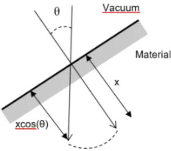
If the primary beam collides normally to the surface we consider its traveling depth to bex. Considering a different angle of incidenceθ, the traveling depth of the primary
electron is stillxbut the point at which the electron stopped from the surface isxcos(θ)
(Figure 2.3). This new distance is shorter, and since secondary electrons are created closer to the surface, the probability of their emission increases according to the expression 2.3, leading to higher SEYs.
Figure 2.3: Correlation between the angle of incidence of primary electrons and their depth.
The other important factor is the roughness of the surface. In a smooth surface, an electron leaving the substrate has no obstacles at all, but in a roughened surface that does not happen. In that case, an electron leaving the surface has high probability to be recaptured by the protrusions (Figure 2.4). This effect leads to fewer ejected electrons from the surface which results in a lower SEY. Nevertheless, it is important to note that rough surface also implies oblique incidence of electrons to the sample, which may also increase SEY. Therefore, depending on the details of the surface topography, rough surface may both increase or decrease SEY.
Figure 2.4: Examples for SEE on grooved surfaces [13].
CHAPTER 2. CONCEPTS AND EXPERIMENTAL TECHNIQUES
kind of materials or with even its own oxide (looking at the oxide as a contaminant), the secondary electron emission properties of the material will be influenced leading to an increasing of its SEY.
2.1.3 Graphene
Graphene is a two dimensional allotrope of carbon consisting of a single layer of carbon atoms arranged in a hexagonal lattice of graphite (Figure 2.5). Layers of graphene stacked on top of each other form graphite. It is the thinnest known compound with only one atom thick as well the lightest and the strongest compound discovered [17]. Graphene has unique electronic, mechanical, optical and thermal properties, among others, which makes it suitable to a very wide range of applications.
Figure 2.5: Hexagonal lattice of graphene.
2.1.3.1 Carbon Hybridization
Hybridization of atomic orbitals occur when atoms get ready to form bonds. It is when s and p orbitals merge together in order to create new lower energy sp orbitals. s and p orbitals combine with each others and allow an overlapping of the orbitals forming hybrid orbitals. Two different atoms having the same hybrid orbitals, come together resulting in an overlapping of these orbitals and a formation of a covalent bond.
There are three types of carbon hybridization (sp1,sp2andsp3) but only two will be
explained since these are the ones that will be observed.
• sp3Hybridization
Carbon atoms have the following electron configuration: 1s22s22p2. So, there are
only two p orbitals that have unpaired electrons. For carbon being able to form such molecules asCH4(methane) or even a diamond structure, four equivalent bonding
orbitals need to be created. This happens naturally when mixing one s orbital with the three p orbitals, producing four hybrid orbitals calledsp3orbitals.
2.1. FUNDAMENTAL CONCEPTS
These new orbitals are arranged in a tetrahedron shape (Figure 2.6). After the hybridization, all four orbitals have the same energy, lower than p but higher than s orbitals.
Figure 2.6:sp3hybridization tetrahedron shape [18].
In this configuration, all four valence electrons of carbon are occupied to form bonds, they are localized in between atomic nuclei. Consequently, there are no electrons left to conduct electrons. This is why compounds withsp3carbon are dielectrics, they
have energy gaps: four electrons form valence band and conductance band is empty.
• sp2Hybridization
Graphene has a honeycomb 2D shape, so it means that each carbon atom has three bonds to other carbon atoms. In this case, three atomic orbitals are mixed to form three new hybridized molecular orbitals. These new orbitals are calledsp2hybridized
orbitals, since the s and two of the three p orbitals are combined.
1s22s2 2p2 −→ 1s2sp12 sp12sp12 2p1z
Because one of the p orbitals has not changed, its energy is higher than the sp2
orbitals. Since 3 electrons form bonds (sp2orbitals), the one (pz orbital) is left and
contributes to the electric conductivity. For example, graphite is a metal with zero electron density at the Fermi level. This way, there are three identical bonds and due to the symmetry they have a planar trigonal geometry with 120 degrees between each other, while the remaining p orbital stays normal to its plane (Figure 2.7). In the case of graphene, only three bonds are made through thesp2orbitals, leaving
the p orbital electron "quasi-free" and responsible for the electrical conductivity.
2.1.3.2 Production Techniques
CHAPTER 2. CONCEPTS AND EXPERIMENTAL TECHNIQUES
Figure 2.7: Trigonal planar geometry ofsp2hybridization [19].
1. Chemical Vapor Deposition (CVD)
CVD is one of the standard techniques for graphene production. The apparatus consists of a tubular furnace where high temperatures are achieved (900-1000◦C).
Firstly an inertAr/H2gas is introduced through the furnace for impurities removal
that might prevent the graphene growing. Then, the hydrocarbon gas (usually methane,CH4) is introduced (carbon precursor). At the high temperatures achieved,
the hydrocarbon gas decomposes into carbon and hydrogen. The formed carbon is deposited on a copper catalyst and forms a honeycomb structure of graphene. The metal surface acts as a catalyst, so, as soon as it is covered, the catalytic effect stops. Hence the technique is more convenient to grow a single layer of graphene. These catalytic properties are only common to certain metals, which is why copper is used as a catalyst [20].
Figure 2.8: Scheme of standard CVD grown graphene [20].
2. Microwave atmospheric plasma based synthesis
In comparison with CVD, plasma assisted techniques have their own advantages in carbon nanostructures’ synthesis. Plasma systems possess thermal and chemical reactor functions. Using plasma to assist the growing of graphene, a catalyst is not needed, opposing the case of CVD. Plasmas have the unique ability to create favorable conditions for nucleation and growth processes [21].
A hydrocarbon gas (ethanol vapour,C2H5OH) is injected into the chamber together
2.2. EXPERIMENTAL TECHNIQUES
carbon atoms and molecules are created. These carbon atoms and molecules migrate to the colder plasma regions, resulting in the nucleation of solid carbon nuclei. "The main stream of carbon nuclei is gradually withdrawn from the hot plasma region into the outlet plasma stream, where flowing carbon nanostructures assemble and grow" [21]. By adjusting the microwave plasma environment, it is possible to achieve the synthesis of free-standing graphene platelets (stacks of graphene with 10 to 20 layers) [21]. IR heaters and UV irradiation are used to tune the thermodynamical conditions in the nucleation zone.
Figure 2.9: Process scheme of microwave atmospheric plasma based production of free standing graphene [22].
2.2
Experimental Techniques
This section is divided in four subsections describing the following techniques: Elec-trophoretic Deposition - EPD, X-ray Photoelectron Spectroscopy - XPS, SEY measurement and Scanning Electron Microscopy - SEM. EPD is used to make the graphene coatings, XPS for characterization of the surface, SEY apparatus for SEY measurement and finally SEM for the surface morphology analysis.
2.2.1 Electrophoretic Deposition - EPD
Electrophoretic Deposition consists of a dispersed powder material in a certain solvent (electrolyte) and with an applied electric field, the powder particles are able to move into a desired arrangement on an electrode surface (Figure 2.10). The electrolyte charges the surface of the dispersed particles enabling these to move according to the applied electric field. The charging process occurs via the formation of an electrical double layer (Figure
CHAPTER 2. CONCEPTS AND EXPERIMENTAL TECHNIQUES
between the particles and the fluid (zeta potential).
Figure 2.10: Schematic of EPD phenomena [23].
Zeta potential is the electric potential in the interface of the double layer with the fluid (Figure 2.11). It is a key factor since it plays a role in the stability of the suspension, the direction and migration velocity of particles and the density of the deposit [24]. The stability of the suspension depends on the interaction between particles, which are driven by Coulomb and Van der Waals forces. These forces define the interaction between the particles - whether if the suspension will be stable or not, and whether it will be able to deposit. The particle charge also affects the density of the deposit. If the charge is too low, particles tend to agglomerate, while if the charge is too high, particles will repulse each other leading to a non-efficient deposition. Therefore, it is important to control the zeta potential in order to achieve an efficient EPD.
Figure 2.11: Diagram of double layer and zeta potential of a particle in an ionic fluid [25].
There are four main characteristics that define EPD:
1. Particle dispersion
2.2. EXPERIMENTAL TECHNIQUES
is important that the particle dispersion stays stable from the end of the dispersing process (sonication) to the end of the deposition. The dispersion of particles depends on Van der Waals forces, on the Debye length and the amount of charge in the first layer.
2. Particle charging
The particles gain a surface charge due to the electrolyte composition where ad-sorption/dissolution equilibrium for anions and cations need to be different. This results in selective dissolution and adsorption of ions from the particle and the solvent, respectively. Both require a solvent able to support ionic charge (electrolyte). There are solvents that behave like dielectric which do not support dissolved ions, however, in EPD, solvents need to support dissolved ions since particles have to be electrochemically charged [26]. This factor directly affects the previous one.
3. Electrochemical migration
An electric field is essential for particles in a suspension can electrochemically migrate. When a voltage is applied to the dispersion, the charged particles migrate to the opposite charged electrode, where an electrostatic boundary layer is formed. This created layer will shield the electrode’s charge. similarly to a plasma, resulting in a null electric field in the bulk of the suspension [26]. This way, the electric field is confined to the boundaries of the electrode (Figure 2.12).
Figure 2.12: Simulation of the electric field around the electrode [23].
4. Deposition of particlesDue to electrochemical changes occurring at the electrode,
there are different phenomena that can change the balance of the dispersed particles, leading to their repulsion between each other in the suspension and their deposition at the electrode.
CHAPTER 2. CONCEPTS AND EXPERIMENTAL TECHNIQUES
there is too much charge, deposition does not occur, because particles will repel each other. This results in short Debye length of the electrodes and lack of field in the suspension.
It was also discovered that there is a narrow margin of conductivity (which is different for every system) suitable for EPD. For this reason, the conductivity of the suspension needs to be carefully controlled in order to be able to use the technique. So, according to the theory, particles move and are deposited together with the ions, which stay attached to the particles.
There is one other type of electrochemical process that can be similar and easily con-fused with EPD, but is fundamentally different from it. This other technique is called electrodeposition (electroplating). This technique produce coatings by diffusion and migra-tion of ions or molecules from one electrode to the other, where they are electrochemically converted into an insoluble form [26]. Typically there are dissolved metal cations, which are produced at the anode, that flow to the cathode resulting in their reduction, and consequently, in the formation of a thin uniform metal coating.
Table 2.1resumes the main differences between EPD and electroplating.
Table 2.1: Main differences between EPD and Electroplating [26].
Deposition Technique Electrophoresis Electroplating
Moving Species Solid Particles Ions Charge Transfer None Ion Reduction Required Conductance of Liquid Medium Low High
Sometimes there is a type of corrosion where small cavities (pits) are created on the surface of a metal and can go all the way through without losing any thickness. They are extremely localized and their main source is the location of the oxides on the surface. If the surface is anodic, the areas where there is excess of oxygen become cathodic leading to a localized corrosion creating pits. This type of corrosion is called pitting.
2.2.1.1 Factors influencing EPD
Electrophoretic deposition deals with suspended charged particles under the influence of an electric field. There are two main groups of factors that may influence EPD: the parameters related to the suspension and the parameters related to the process [24].
In suspension properties, characteristics of the liquid such as of the suspended particles, must be considered.
• Particle size
According to [28], particle size in range of 1-20µm for ceramics and clay particles,
2.2. EXPERIMENTAL TECHNIQUES
due to gravity. This usually results in a non-uniform coating, where the bottom part of the electrode is thicker than the upper (for vertical electrodes). For this reason, particles must remain well dispersed in order to assure good mobility and uniform coatings.
• Suspension’s stability
The stability of the suspension is important for dispersed particles to move when an electric field is applied. Particles which are 1µm wide, or less, tend to remain
dispersed, while particles above that size require continuous hydrodynamic motion. The stability is defined by the settling rate and tendency to avoid agglomeration, where a stable suspension shows no tendency to flocculate and settles slowly [24]. In that sense, stability is directly related to particle charge or zeta potential i.e. about the potential distribution between particles (interplay between Van der Waals and Coulomb forces).
There is one main parameter related to the process in this work, that may influence the EPD: the applied potential to the electrodes. Usually, an increase of applied voltage leads to higher deposition rates, which increases the amount of deposit, but its quality may suffer [24]. According to [29], moderate applied electric fields result in more uniform deposits, while the opposite occurs for increasing applied potentials. The increasing of the applied voltage may cause turbulence in the suspension leading to undesirable flows in the fluid, which disturb the deposition process. Due to the higher depositions rates, particles might move too fast and they would have not enough time to properly fix to the electrode. In conclusion, the applied potential directly influences particle flux, consequently affecting the deposition rate and the structure of the deposit [24].
2.2.1.2 Home-made EPD system
The home-made apparatus built for electrophoresis is composed of 4 pieces (Figure 2.13):
• Electrodes: two metal plates responsible for creating the electric field. They are both
20x10 mm and they are 15 mm away from each other. Flat plates were chosen so they could be measured properly in XPS, SEM and SEY. The counter electrode (uncoated) is gold, one of the most inert metals for electrolysis, despite stainless steel was also used, and the coated electrodes were stainless steel and copper.
• Conductive rods: these are two identical copper wires, 2 mm thick, where the
electrodes are attached on one end. The opposite ends are connected to the power source
• Rubber support: this piece is responsible for holding everything together.
CHAPTER 2. CONCEPTS AND EXPERIMENTAL TECHNIQUES
• Glass cup: the glass cup is needed to sustain the electrolyte and it is where the
rubber support is attached.
Figure 2.13: Home-made apparatus for EPD.
2.2.2 SEY apparatus
2.2.2.1 Operation Principles
The apparatus measures the secondary electron yield by measuring independently the emitted and incident current. In this setup, sample is mounted on a sample holder, which is placed inside of a Faraday cup. Initially, the sample holder is negatively biased (-V), to repel secondary electrons from the sample and suppress the arrival of the second generation of secondary electrons produced on the walls of the Faraday cup. That way, the secondary electron current generated by the sample is measured by the Faraday cup (IFC). This measurement has the contribution of secondary electrons (Is) and backscattered
electrons (Ib) (Figure 3.3: left).
IFC = Is+Ib (2.12)
Secondly, a shortcut is made between the sample holder and the Faraday cup and the current is again measured. Since everything is now connected (sample holder becomes integral part of the Faraday cup), the primary electron current (Ip) is measured (Figure 3.3: right).
With these two measured currents, SEY is the quotient between the first and the second magnitude.
δ = IFC
Ip =
Is+Ib
2.2. EXPERIMENTAL TECHNIQUES
Figure 2.14: Measuring method of primary and secondary currents [4].
2.2.2.2 Instrumentation
The home-made apparatus for SEY measurement is composed of few main elements (Figure 2.15) that will be identified ahead:
• External support(Figure 2.15: yellow): this component is responsible for holding
everything together. It is split into two parts so it can be possible to exchange samples. Its closed structure provides electrical shielding of the whole system and therefore reduces the noise.
• Insulating cylinder(Figure 2.15: light grey): this cylinder is made of alumina which
provides an electric isolation between the Faraday cup and the external support. This isolation is very important so the measurement of both currents can be correctly made.
• Sample holder(Figure 2.15: dark grey): this is the piece where the sample mounted.
It is supported by a small alumina cylinder so it can also be isolated from the Faraday cup to prevent a shortcut between them. As already explained, the sample holder can be shortcut to the Faraday cup or biased negatively to help the secondary electrons being ejected from the sample into the Faraday cup and to suppress arrival of the secondary electrons from the Faraday cup to reach the sample (and therefore decrease the measured current of secondary electrons from the sample).
• Electron gun(Figure 2.15: dark blue): this part is a typical electron gun with an
hairpin geometry filament followed by electron optics for the beam focusing.
• Suppressor electrode(Figure 2.15: light blue): this electrode is negatively biased so
CHAPTER 2. CONCEPTS AND EXPERIMENTAL TECHNIQUES
• Faraday Cup(Figure 2.15: green): the cup is also split into two parts with the same
purpose as the external support. The Faraday cup is the detection system of the apparatus since it is the electron collector. The current generated is measured by an electrometer connected to the cup.
Figure 2.15: Instrumentation layout of the homemade apparatus for SEY measurement [4].
2.2.2.3 Measuring Errors
The secondary current Is in SEY is the current generated in the Faraday cup by the
secondary electrons emitted from the sample surface (when the sample is biased) or the primary electron sample (when the sample and the Faraday cup are in shortcut). In an ideal case, when the electron beam only hits the sample, the main measurement error is related to the electron beam stability and the measurement uncertainty of the two currents. However, frequent work with the equipment revealed another potential systematic error, which takes place when part of the primary electron beam misses the sample and hits the bottom of the Faraday cup (Figure 2.16). The amount of this error can be analytically estimated.
Primary current Ip is defined as the current generated by the electrons that hit the
sample, ISp, plus the ones hitting the Faraday cup,IpF:
Ip= IpS+IpF (2.14)
Being IS
p = (1−k)Ip and IpF = kIp, assuming k is the fraction of primary electron
current that misses the sample. Using equation (2.14):
2.2. EXPERIMENTAL TECHNIQUES
Figure 2.16: Illustration of SEY measuring errors.
In that sense, the measured secondary current is the sum of two contributions: the primary electrons that hit directly the Faraday cup (miss the sample),IF
p, and the secondary
electrons generated on the sample.
Is= IpF+IpSδ (2.16)
withδ = IS
IS
p being the real SEY of the material. So, combining equations (2.15) and
(2.16),
Is=kIp+ (1−k)Ipδ (2.17)
Consideringδexpwhat is really measured:
δexp= Is Ip
= kIp+ (1−k)Ipδ
Ip
=k+ (1−k)δ (2.18)
Taking equation (2.18) into consideration, some conclusions can be drawn:
• Ifδis below 1, the measured magnitudeδexpis greater than the true value;
• Ifδis above 1, the exact opposite occurs,δexpis lower than the expected value;
• If k is 1, which means the beam is completely missing the sample,δexpis going to be
exactly 1;
• Finally, if the entire beam hits the sample (k=0), thenδexp= δ.
CHAPTER 2. CONCEPTS AND EXPERIMENTAL TECHNIQUES
2.2.3 X-Ray Photoelectron Spectroscopy
2.2.3.1 Operation Principles
XPS is based on the photoelectric effect but the irradiation of the sample can lead to the occurrence of two different phenomena: emission of photoelectrons and Auger electrons (Figure 2.17). The X-rays interact with the atoms of the surface, exciting them, and if they have enough energy, they are ejected from the inner shells of the atom. These photoelectrons have a kinetic energy (Ek) equal to the difference between the X-ray energy
(hν), the binding energy of the emitted electrons (Eb) and the work function of the energy
analyzer:
Ek(e−) =hν−Eb−WFanal (2.19)
After the ionization, the electron cloud can rearrange itself by radiative or non-radiative processes. In the second case, the ion has some potential energy which is spent to the emission of electrons. The driving force for the emission is Coulomb repulsion between the two electrons in the atom. This emitted electron is called Auger electron.
EI JK(e−A) =EbI−EbJ−EbK−WFanal (2.20)
whereEbI,EbJand EbKare respectively the binding energies of the core level (from
where the inner electron was ejected), first outer shell, and second outer shell (energy level where Auger electron came from).
The XPS spectra will be mainly composed of photoelectronic peaks but will also have Auger electron contributions resulting in two different kinds of peaks in a final spectrum.
Figure 2.17: Schematic of photoemission process and Auger effect.
2.2. EXPERIMENTAL TECHNIQUES
The binding energy of the emitted electrons depends on their main quantum number and total angular momentum j:
j=l+s (2.21)
in whichEbdecreases with j. Therefore, for each single electron orbital there are two
lines corresponding to the two values of the angular momentum. The exceptions are s orbitals (l=0) when the total angular momentum can be onlyj=1/2. There are 2j+1 degenerate states per each j, which provides the correlation between the number of states and the intensity ratio between the two peaks attributed to a single electron orbital. For example, if an electron ejected from a p level reaches the detector, it will result in two spectral lines (j =3/2 andj = 1/2), so that the 3/2 peak has twice the intensity of the 1/2 peak (2:1). The intensity ratios between the lines having the same main and orbital quantum number are summarized in Table 2.2.
Table 2.2: Correlation between the degenerate states and respective intensity ratios.
Energy level l j Intensity ratio
s 0 1/2
-p 1 3/2 1/2 2:1
d 2 5/2 3/2 3:2
f 3 7/2 5/2 4:3
2.2.3.2 Instrumentation
The X-ray photoelectron spectrometer has 4 main components (Figure 2.16):
1. X-Ray source: the apparatus that will be used has a double non-monochromatic
anode source of Al/MgKα. The advantage of these kind of sources, besides the
pos-sibility to change between anodes, is that it facilitates the charge accumulation effect on the non-conductive samples, but its resolution is worse than of a monochromatic source. The two anodes have similar photon energies to observe the differences between Auger and photoelectric peaks. In the kinetic energy scale, photoelectric peaks shift for different photon energies and Auger peaks do not. In the binding energy scale, they have the opposite behavior.
2. Hemispherical energy analyzer: this type of analyzer only allows electrons of a
CHAPTER 2. CONCEPTS AND EXPERIMENTAL TECHNIQUES
3. Electron detector: the signal generated by the electrons that reach the detector is
converted in an electric signal. To do so, it is used a Channel Electron Multiplier (CEM) or Channeltron.
4. Vacuum System: ultra-high vacuum is necessary to keep the surface of the sample
clean and for an efficient functioning of the X-ray source. Surface cleanness is es-sential due to the very high surface sensitivity of the technique: the information depth of XPS is typically 5-10 nm. Another reason to keep the system under vacuum, although less demanding than the other two, is to increase the mean free path of the electrons on their way from the sample to the detector.
Figure 2.18: Instrumentation layout of a typical XPS instrument [30].
2.2.3.3 Chemical Information
Composition Determination
Elemental composition analysis can be obtained from the intensities of characteristic peaks of each element at the surface. The peak intensity of an element,Siis proportional
to: photon flux, I (m−2s−1), acquisition time per energy channel,∆t(s), analyzed area, A
(m2), photoemission cross-section,σν(m2), effective attenuation length,λi(m), detection
efficiency, D, transmission of the spectrometer, T, and concentration of the element,ni
(m−3) [31]. Assuming uniform depth distribution of the concentration (ni(z) = Ni), the
total XPS signal can be calculated from,
Si = I·∆t·A·D·T·σi·λi·Ni (2.22)
2.2. EXPERIMENTAL TECHNIQUES
sensitivity factors (SF) may be determined by performing measurements on a reference sample.
SFi =
Sre fi
I·∆t·Nire f = A·D·T·σi·λi, (2.23)
whereNire f is the bulk concentration of the reference sample.
It is more convenient to define sensitivity factors relative to one element, for that purpose, fluorine is frequently used (RSFF = 1.0). Consequently, relative sensitivity
factors of any element is defined as
RSF = SFi
SFF
= S
re f i /N
re f i
Sre fF /NFre f (2.24)
Finally, relative concentration of an element ’i’ is determined as
ci = Si
/RSFi
∑(Sj/RSFj)
(2.25)
where index ’i’ is related to the element and ’j’ to all elements identified in the sample. This last formula is used for composition analysis in XPS in the vast majority of cases.
Chemical Shifts
The chemical shift of photoelectron peaks is related to the difference in position of a photoelectron peak for atoms of the same element in different chemical environments. For example, considering a lithium atom in a clean metal (Li) and in its oxide (Li2O): due to
the electronegativity of the oxygen (O), the valence electrons of Li will move towards the O atoms. The remain electron in the Li atoms will have higher binding energies due to the lack of electrons which partially screens the attractive force of the nucleus. This effect leads to higher binding energies in the clean metal compared to theLi2O, which means
there is a shift of the lithium peak in that direction [32].
Modified Auger electron parameter
CHAPTER 2. CONCEPTS AND EXPERIMENTAL TECHNIQUES
Shake up Satellites
Usually it is assumed that there is no rearrangement of the electron cloud after an electron emission. In this case, the electron binding energy is the same as the energy of the level where it came from. In some cases, there is a probability that some of the photon energy is spent exciting an electron from upper levels. In this situation, the energy of the photoelectron is reduced, which results in a higher binding energy and the respective peak is preceded by a shake-up satellite. At first sight, this energy loss complicates the spectrum analysis but the position and the intensity of the shake-up satellites strongly depend on the chemical bonds, so these can be used as fingerprints of some chemical compounds [34].
Multiplet Splitting
Multiplet splitting occurs when an atom has unpaired electrons. When an inner shell electron vacancy is created by photoionization, an unpaired outer shell electron can be coupling with the unpaired core electron. These phenomena create different final states which contribute to a multipeak envelope in the final spectrum [31]. Cr 2p3/2line for a Cr2O3sample is a good example of multiplet structures (Figure 2.19).
Figure 2.19: Multiplet structure associated with the Cr 2p3/2 peak for a vacuum fractured Cr2O3specimen [35].
Profile Lines
In XPS analysis, a wide variety of line profiles can be used to fit XPS spectra, and simple Gaussian or Lorentzian functions are very rarely used. In some cases, asymmetric profiles are theoretically expected, but due to instrumental and physical effects, real XPS data show some deviations from the theory [36]. Some of these effects can be: the response function of the analyser, profile of the X-ray line-shape (dependent of whether it is monochromatic or non-monochromatic), differential surface charging of the sample, among others.
2.2. EXPERIMENTAL TECHNIQUES
• Gaussian-Lorentzian(product) - GL(p)
This profile is a pseudo-Voigt profile in the form of a product of Gaussian and Lorentzian. Voigt profile is the convolution of Gaussian and Lorentzian, but this integral does not have analytical solution. That is the reason why Voigt profile has to be simulated as a product of G and L, (GL profiles) or as a sum of G and L (SGL profiles). So these are approximations of the Voigt profile which is theoretically expected in many cases. GL(p) is a Gaussian/Lorentzian product where the mixing is determined by p (percentage of Lorentzian contribution). So GL(100) is a pure Lorentzian while GL(0) is pure Gaussian [36].
GL(x,F,E,m) = exp(−4ln(2)(1−m)
(x−E)2
F2 ) 1+4m(x−F2E)2
(2.26)
Throughout this work, this line shape is used to fit almost every peak and its contributions in XPS spectra.
• Doniach-Šunji´c - DS(α,n)
DS(α,n) is a basic Doniach-Šunji´c profile convoluted with a Gaussian.αis an
asym-metry parameter and n is the the convolution width, related to the Gaussian’s width. This profile is theoretically predicted for the photoelectron lines emitted from metal-lic samples. Convolution with Gaussian is used to include the contribution of the finite resolution of the energy spectrometer. This line shape is typically used for fitting doublets, and it will be used further to model the Au 4f doublet profile.
DS(x,α,F,E) = cos[
πα
2 + (1−α)tan−1(x−FE)]
(F2+ (x−E)2)1−α
2
(2.27)
• Hybrid Doniach-Šunji´c/Gaussian-Lorentzian(product) - H(a,n)GL(p)
H(a,n)GL(p) is a hybrid form of DS/GL convolution an it is similar to DS(a,n)GL(p), only differing the FWHM and area parameters that are determined by the curve shape. The asymmetry parameter, a, is defined as
a =1− f whmle f t f whmright
This hybrid profile is use to fit the C1s graphitic line. The parameters were deter-mined by us from fitting C 1s line of Highly Oriented Pyrolytic Graphite (HOPG), using it as a reference for C 1s ofsp2carbon.
2.2.4 Scanning Electron Microscopy
2.2.4.1 Operation Principle
CHAPTER 2. CONCEPTS AND EXPERIMENTAL TECHNIQUES
consists in using an electron beam, guided by a deflection system that allows a scanning of the sample’s surface. The electrons of the beam can be produced by a heated filament that works typically from 1 to 50 kV, or by field emission where emission of electrons is induced by an electrostatic field. The created electrons are accelerated and focused on the sample.
Once the electrons interact with the material of the sample, three types of phenomena are used to characterize it (Figure 2.20):
1. When primary electrons hit a bound electron (Figure 2.20: left), they can ionize the atom by ejecting an electron. As the matter of fact, the closer is the binding energy to the primary ion energy the higher is the ionization probability. But then the ejected electron, with much less energy, will go away. Finally, after several generations, many slower electrons which loose their energy through different processes, are responsible for generating secondary electrons.
2. Backscattered electrons are electrons emitted from the surface with energy above 50 eV. These electrons are primary electrons that lose, or not, some of their energy before being backscattered (Figure 2.20: middle).
3. High energy primary electrons can excite inner shells electrons, creating a hole. One of the electrons from the orbitals immediately above descends and occupies the vacancy. This transition results in the emission of electromagnetic radiation (characteristic X-rays) (Figure 2.20: right).
All of these effects have their respective detection systems which contribute in their own way for the imaging process.
Figure 2.20: Mechanisms of secondary electrons emission, backscattered electrons, and characteristic X-rays from SEM’s samples [37].
2.2.4.2 Instrumentation
A typical SEM instrument has a few main components that are fundamental for the equipment (Figure 2.21):
• Electron gun: the electron gun is composed of an electron emitter, where the
2.2. EXPERIMENTAL TECHNIQUES
• Focusing system: this is a set of electrodes responsible for the focusing of the electron
beam.
• Scanning coils: these are deflection coils which are placed at the end of the focusing
system and its function is to deflect the beam in the xy plane so it can scan and raster an area of the sample surface. Magnetic fields typically produce much stronger force than electric fields. When dealing with very fast electrons, a huge force to deflect them is needed. It is much easier to do that by a small applied current in a coil than by a great applied voltage to deflection plates.
• Detection system: usually there are two types of detection systems, secondary
elec-tron detector which is indispensable, and a backscattered elecelec-tron detector. The secondary electron detector is used to distinguish between areas with different depths, where darker areas are deeper than the brighter ones. This is explained by low secondary electron emission from deeper zones (dark areas) where secondary electrons are recaptured, while superficial areas have higher secondary electron emission (brighter zones). The second detection system is used to detect contrast be-tween areas with different chemical compositions. Since heavy elements backscatter electrons more strongly than light elements, resulting in brighter areas on the image. It can also have an x-ray detector so it can perform EDS (Energy Dispersive X-ray Spectroscopy) for chemical analysis.
• Vacuum system: electronic microscopes should operate at least at 10−6mbar. This
guarantees a longer free mean path, for the secondary electrons to travel from the sample to the detector, eliminate discharges between the anode and the cathode and extends the filament “life”. Ion pumps secure the best pressure in the region close to the electron source, where the acceleration takes place. The necessity of vacuum makes it impossible to scan wet samples.
C
H
A
P
T
E
R
3
E
XPERIMENTAL
P
ROCEDURES
There are two important experimental procedures that are worth to be described: the production of the coatings by EPD and the SEY measurement.
3.1
EPD procedure
The EPD technique was chosen because it was proven that graphene coatings by EPD could reduce the SEY of a surface material [3]. Since it is an extremely simple and cheap technique and can be applied to both small and large scales, it was a very promising option. For that reason an EPD cell was built (Section 2.2.1.2). The various choices and parameters used in this technique were a combination of different references in the literature.
Firstly, the choice of electrodes was made according to the interest of this work. It was used copper (Cu) and stainless steel (SS) plates, 0.4 and 1 mm thick, respectively, as the coated electrode and a gold (Au) foil, 0.1 mm thick, as the counter electrode. Gold or gold coated electrodes are commonly used in electrophoretic deposition because it is one of the few materials that are most inert to electrochemical processes, similar to platinum [39].
CHAPTER 3. EXPERIMENTAL PROCEDURES
times and equipments), trying to reproduce the procedure in [3], an alternative had to be taken. In that sense, an experiment of trying to combine both studies was made. Instead of water as a dispersive agent, isopropanol was used. It was possible to successfully disperse free standing in IPA in about 30 seconds, leading to a completely homogenuous black dispersion. The only problem with this choice of solvent is the fact that the suspension only stays stable for approximately 15 minutes, having the need to be sonicated every 15 minutes.
The next step was to add the source of ions to make the electrolyte, so, 20µL of HCl
were added to the 7.5 mL of isopropanol. The amount of HCl was studied according to the current obtained in the deposition process and the amount of chlorine (Cl) contamination on the coating. For that reason, an amount between 10 and 20 µL was the minimum
amount to get a minimal stable current and the maximum amount to not get significant chlorine contamination (<1%).
Finally, it had to be studied the voltage at which the process was possible. The study of the used voltage and the amount of HCl in the electrolyte were made together. Different voltages were tested regarding different amounts of HCl in the solution. In order to get cur-rent, the voltage regarding the process or the amount of HCl needed to be increased. Since the amount of HCl was chosen, because of the reasons explained above, the minimum voltage which enables to coat was found. It was concluded that 20V was the minimum voltage to get some kind of current in the "inner" circuit of EPD, resulting in 0.01 A with the 20µL of hydrochloric acid added to IPA.
The entire process can be resumed in just a few steps as illustrated in figure 3.1.
Figure 3.1: EPD procedure diagram.
Firstly, 7.5 mL of isopropanol are poured in the glass cup along with 1.1 mg of free standing graphene. The mixture is sonicated for 60 s in order to disperse homogeneously the graphene. Then, 20µL of HCl are added followed by another 60 s of sonication. Finally,
3.2. SEY MEASUREMENT PROCEDURE
exposure for a few minutes and it is ready to be analyzed and measured.
3.2
SEY measurement procedure
The SEY measurement procedure is much more simple than the previous one. Once the sample has completely dried from the EPD, it is immediately ready to be mounted and put under vacuum. In order to be mounted, some steps need to be taken.
The external support and the Faraday cup are divided into two parts in order to mount and dismount it. Firstly, the bottom part of the external support and the Faraday cup are detached so it is possible to mount the sample on the sample holder. The sample is held with a carbon sticker and a thin wire is attached to both sides of the sticker to ensure electrical contact between the sample and the sample holder. After the sample is mounted, everything is put back together in its proper order, the biasing contacts are checked and the chamber is closed. To create vacuum, two different pumps are used: a diaphragm pump and a turbo/drag pump to primary (∼5−10 mbar) and high vacuum (10−7mbar),
respectively. It is relatively fast to achieve high vacuum, where it is possible to go down to 10−6mbar in approximately 15 minutes. After the necessary vacuum is reached and
all the contacts are checked, the measurement can take place. This process is resumed in figure 3.2.
Figure 3.2: SEY measurement procedure diagram.
Two different power supplies are needed for the biasing: one polarizes the sample to -15 V and the other one the suppressor to -20 V. The sample is biased during the entire process, while the suppressor is grounded from 0 to 100 eV, low energy regime, and it is biased from 100 to 1000 eV (primary energy), high energy regime. An electrometer is connected to the Faraday cup in order to measure the low currents produced, of the order of nA (10−9A). Primary and secondary current are measured independently, via a switch,
CHAPTER 3. EXPERIMENTAL PROCEDURES
are used. So, a total of 44 current values are taken, 22 for Ipand 22 forIs. These values are
then put into a table in any spreadsheet editor allowing an easy calculation of SEY and further drawing of its curve as a function of primary energy (Figure 3.3).
(a) Example of a typical table used for
SEY calculation. (b) Typical SEY curve.
![Figure 2.1: Three steps for the productions of true secondary electrons [4].](https://thumb-eu.123doks.com/thumbv2/123dok_br/16537296.736594/24.892.254.595.355.541/figure-steps-productions-true-secondary-electrons.webp)
![Figure 2.2: Illustration of a typical SEY curve as a function of primary electron energy [16].](https://thumb-eu.123doks.com/thumbv2/123dok_br/16537296.736594/26.892.271.573.665.873/figure-illustration-typical-curve-function-primary-electron-energy.webp)
![Figure 2.9: Process scheme of microwave atmospheric plasma based production of free standing graphene [22].](https://thumb-eu.123doks.com/thumbv2/123dok_br/16537296.736594/31.892.265.664.343.547/figure-process-scheme-microwave-atmospheric-production-standing-graphene.webp)
![Figure 2.11: Diagram of double layer and zeta potential of a particle in an ionic fluid [25].](https://thumb-eu.123doks.com/thumbv2/123dok_br/16537296.736594/32.892.283.568.721.959/figure-diagram-double-layer-potential-particle-ionic-fluid.webp)
![Figure 2.14: Measuring method of primary and secondary currents [4].](https://thumb-eu.123doks.com/thumbv2/123dok_br/16537296.736594/37.892.251.688.136.402/figure-measuring-method-primary-secondary-currents.webp)
![Figure 2.15: Instrumentation layout of the homemade apparatus for SEY measurement [4].](https://thumb-eu.123doks.com/thumbv2/123dok_br/16537296.736594/38.892.325.528.274.554/figure-instrumentation-layout-homemade-apparatus-sey-measurement.webp)

![Figure 2.18: Instrumentation layout of a typical XPS instrument [30].](https://thumb-eu.123doks.com/thumbv2/123dok_br/16537296.736594/42.892.295.552.419.685/figure-instrumentation-layout-typical-xps-instrument.webp)
![Figure 2.19: Multiplet structure associated with the Cr 2 p 3/2 peak for a vacuum fractured Cr 2 O 3 specimen [35].](https://thumb-eu.123doks.com/thumbv2/123dok_br/16537296.736594/44.892.316.532.568.799/figure-multiplet-structure-associated-peak-vacuum-fractured-specimen.webp)
