Mariana Amorim Fraga*
Technological Institute of Aeronautics São José dos Campos – Brazil [email protected]
Rodrigo Sávio Pessoa
Technological Institute of Aeronautics São José dos Campos – Brazil [email protected]
Homero Santiago Maciel
Technological Institute of Aeronautics São José dos Campos – Brazil [email protected]
Marcos Massi
Technological Institute of Aeronautics São José dos Campos – Brazil [email protected]
Ivo de Castro Oliveira
Technological Institute of Aeronautics São José dos Campos – Brazil [email protected]
*author for correspondence
Technology roadmap for
development of SiC sensors at
plasma processes laboratory
Abstract: Recognizing the need to consolidate the research and development (R&D) activities in microelectronics ields in a strategic manner, the Plasma Processes Laboratory of the Technological Institute of Aeronautics (LPP-ITA) has established a technology roadmap to serve as a guide for activities related to development of sensors based on silicon carbide (SiC) thin ilms. These sensors have also potential interest to the aerospace ield due to their ability to operate in harsh environment such as high temperatures and intense radiation. In the present paper, this roadmap is described and presented in four main sections: i) introduction, ii) what we have already done in the past, iii) what we are doing in this moment, and iv) our targets up to 2015. The critical technological issues were evaluated for different categories: SiC deposition techniques, SiC processing techniques for sensors fabrication and sensors characterization. This roadmap also presents a shared vision of how R&D activities in microelectronics should develop over the next ive years in our laboratory.
Keywords: Silicon carbide, Sensors, Aerospace applications, Roadmap, Project planning.
INTRODUCTION
Silicon carbide (SiC) has been widely studied as an electronic material since 1959, when Shockley, the inventor of the bipolar transistor, recognized this material as essential to enable the development of microelectronic devices that can withstand harsh environmental conditions where silicon cannot be used or have limited applications such as high temperatures and intense radiation (Shockley, 1959). The potential of SiC for these applications is due to its inherent properties as excellent thermal stability, high resistance to chemical attack, high hardness, high bandgap,
high electric ield breakdown and high saturation current
of electrons (Rajab, 2005).
Several techniques for obtaining thin ilms and bulks of SiC
have been developed. Some companies that manufacture crystalline silicon wafers also offer SiC bulk wafers up to 3 inches in diameter. However, a SiC wafer has an average
price ifteen times more than the Si wafer with the same
dimensions (Muller et al., 2001). Besides the high cost,
another problem of the use of SiC substrates is the dificult
micromachining process and high density of defects (Wu et al., 2001). In this context, there is a crescent interest in
deposition techniques of SiC ilms on Si or SOI (Silicon-On-Insulator) substrates. These ilms can be produced in
crystalline and amorphous forms.
Crystalline SiC ilms are produced by techniques that use
temperatures higher than 1000°C such as Chemical Vapor Deposition (CVD), Molecular Beam Epitaxy (MBE) and Electron Cyclotron Resonance (ECR) (Sarro, 2000). The high temperatures involved in these techniques generally
become impracticable for the processing of these ilms in
conjunction with conventional microelectronics processes. Hence, the plasma-assisted techniques such as Plasma Enhanced Chemical Vapor Deposition (PECVD) and
sputtering, that allow obtaining SiC ilms at temperatures
below 400°C, are very attractive (Prado, 1997). However,
SiC ilms produced at low temperatures are amorphous
and their properties are different from those observed in
crystalline structures. In general, amorphous ilms have
lower elasticity modulus and higher electrical resistivity.
Since the 1970s, many studies have been performed on
doping of amorphous SiC ilms in order to obtain properties
near to crystalline for applications at different types of devices such as photovoltaic cells, optical sensors, diodes
and thin ilm transistors (TFTs) (Spear and LeComber,
1975; Kanicki, 1991; Tawada et al., 1982). Nowadays,
the processes most used to doping of SiC ilms are in situ
doping (during ilm growth) and ion implantation.
In the 1990s, due to emerging MEMS (Micro Electro Mechanical Systems) technology and the increasing demand for sensors operating at temperatures above
300ºC for different applications, SiC ilms and substrates
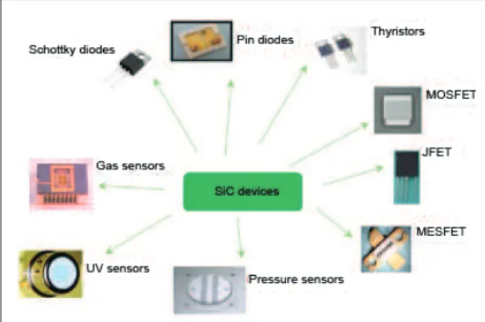
Figure 1: SiC-based devices commercially available.
started to be used as alternatives to silicon in the fabrication of sensors to operate in severe environments as combustion processes or gas turbine control, oil industry, nuclear power and industry process control (Cocuzza, 2004).
Some sensors and electronic devices based on SiC that
are currently commercially available are showed in Fig.1
(Nowak, 2005).
the laboratory by RF magnetron sputtering technique had
appropriate characteristics for applications in electronics and MEMS (Micro Electro Mechanical Systems) devices (Rajab et al., 2006).
In this context, in 2005 a PhD thesis on development of
piezoresistive sensors based on SiC ilms was started
with support from CNPq/Microelectronics National
Program (PNM) (Fraga, 2009). In this thesis, besides the RF magnetron sputtering, the PECVD technique was used to produce the SiC ilms. This allowed comparing the properties of SiC ilms produced by both deposition processes. In addition, the inluence of nitrogen doping on SiC ilm characteristics was also investigated (Fraga et al.,
2008a; Fraga et al., 2008b).
The reactive ion etching (RIE) of SiC ilms using SF6/
O2 gases mixtures was another process studied, because
this step is very important in the fabrication of devices.
The etching rate was investigated as a function of ilm composition and O2 concentration. The inluence of
thermal annealing on etching characteristics was also
evaluated (Fraga et al., 2007a; Fraga et al., 2007b).
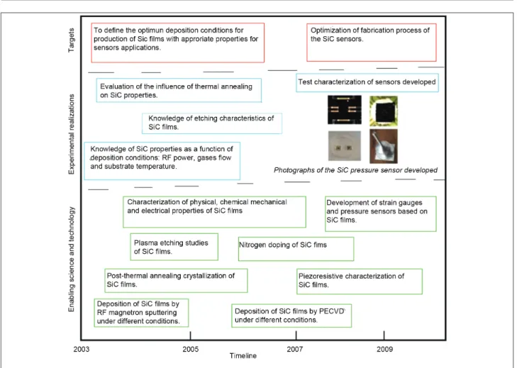
The evolution of R&D activities related to the development
of SiC ilms at Plasma and Processes Laboratory is summarized in Fig. 2.
In 2008, in order to make possible the development of
devices based on SiC ilms, a collaboration project was established with the Microfabrication Laboratory of the Brazilian Synchrotron Light Laboratory (LNLS). The irst devices developed through this project were strain gauges based on SiC ilms. The structure of these strain gauges consists of a SiC thin-ilm resistor with Ti/Au electrical contacts (Fraga et al., 2010a). Subsequently,
a prototype of piezoresistive sensor based on SiC ilm was designed, fabricated and characterized (Fraga et al., 2010b).
The development cycles of the SiC sensors are shown
in Fig. 3. As it can be observed, two steps have not been performed in LPP-ITA yet: pattern transfer by
photolithography and wire bonding process.
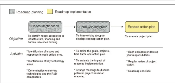
CURRENT STAGE OF R&D ACTIVITIES
The current stage of R&D activities at LPP-ITA aims to
implement a technology roadmap for development of SiC
sensors (Fig. 4). In this section, the roadmap development
process is explained.
The development process is divided into the following stages.
As there is a great interest in the use of SiC in high temperature devices, especially for applications in
aerospace and aeronautics ields, LPP-ITA has established
a R&D line oriented to the development of SiC sensors as presented in the next sections.
ANTECEDENTS OF R&D ACTIVITIES IN MICROELECTRONICS
Since 1988, LPP-ITA has carried out research projects on plasma technology applications. One of the main research lines in this ield is directed to synthesis and modiication of semiconductor thin ilms through low temperature plasma processes such as radiofrequency (RF) magnetron
sputtering, plasma enhanced chemical vapor deposition (PECVD), reactive ion etching (RIE) and inductively coupled plasma (ICP).
The R&D activities in microelectronics were intensiied in
2001, when a clean room environment was implemented
through a inancing of the São Paulo Research Foundation (FAPESP). The development of speciic researches related to growth and characterization of SiC thin ilms
were started in 2003 leading to a master thesis about the effect of thermal annealing on physical and electrical
properties of SiC ilms (Rajab, 2005). This project
was supported by a grant from CNPq/Microelectronics National Program (PNM). The results obtained during
Figure 2: Evolution of R&D activities related to development of SiC ilms at Plasma Processes Laboratory.
Needs identiication
This is the irst stage of the process in which occurs the identiication of the needs related to the SiC sensors
technology development. These needs are grouped in
three main categories: infrastructure, inancing and human
resources.
Nowadays, the Plasma and Processes Laboratory counts on inancing of the Brazilian Space Agency (AEB) to
assemble a room for characterization of electronics and MEMS devices. Besides, the clean room facilities have
been ampliied with the recent acquisitions of an oxidation furnace, a KOH etching system and a hot plate through the inancial support of the National Council for Scientiic
and Technological Development (CNPq). Additionally, a dual dc magnetron sputtering system for the growth
of SiC ilms, from targets of silicon and carbon, is being
implemented. The idea of this system is to control the stoichiometry and improves the quality/functionality of
the ilms through use of pulsed dc power sources. The main needs associated with infrastructure are the clean room area enlargement and the acquisition of a mask aligner in order to perform all steps of sensors fabrication in the laboratory.
In relation to human resources, since December 2009 the
National Post-Doctoral Program (PNPD)/CAPES inances
two grants on development of SiC sensors.
Form working group to the development of roadmap
Due to the interdisciplinary nature of SiC sensors technology, researchers from a wide variety of backgrounds
are required to form roadmap working groups. The staff of
Plasma Processes Laboratory consists of 42 members, and
this interdisciplinary background has degrees in physics,
material science, microelectronics and engineering. Five
PhDs and one PhD student of these staff are working at the moment on researches related to SiC sensors.
This working group discussed the framework roadmap and, subsequently, a methodology was adopted considering the itemization of issues and responses to each critical step and
identiication of the key technologies. The determination
of a realistic timeline and of a cost range for the processes implementation was also required.
In order to deine an action plan roadmap, the working
group divided the critical technologies into three categories:
a) SiC deposition techniques;
b) SiC processing techniques for sensors fabrication;
c) SiC sensors characterization.
For each category, the working group will deine goals, the
impact of the technology, the timeframe for development and the execution plan.
Execution action plan
A detailed project plan with indication of roles and responsibilities of each working group member is
being inalized. A funding strategy will be developed to
overcome critical infrastructure issues.
The progress of roadmap execution action plan will be evaluated by regular review of the project status and deliverables. The expectative is that the implementation of this roadmap raises the level of sharing and integration among staff, facilities and services of the laboratory. This
allows that the researchers quickly deine the key services
and that they focus on the technical challenges.
To help its staff keep pace with the changes in science and technology, the laboratory have formed masters and PhDs in plasma physics, materials science and microelectronics.
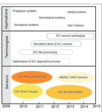
PERSPECTIVES UP TO 2015
The development of the SiC sensors is based on progress in the following technologies: 1) improved electrical and
mechanical properties of SiC ilms produced (optimization of SiC deposition process), 2) SiC ilm processing
(optimization of etching process and metallization appropriate for high temperature applications), 3) microfabrication technology to fabricate miniaturized sensors and 4) sensors packaging for harsh environments.
The R&D activities of the Technological Institute of Aeronautics have been focused on aerospace and
aeronautical ields. In this manner, the goal of Plasma and Processes Laboratory is to develop SiC sensors with
potential for use in a range of these applications. The sensor types of main interest are capable of measuring pressure, strain and acceleration under high temperatures and in the presence of corrosive media or intense radiation.
Figure 5 shows the types of sensors that are being
developed and the technological evolution that we intend to follow till 2015. The main technologies involved and some possible applications also are shown. In the next years, our goals will be concentrated in improving the performance of the SiC pressure sensors and strain gauges developed, besides making possible the development of accelerometers and SAW sensors based on the aluminum
nitride (AlN) ilms deposited on SiC.
CONCLUSIONS
The vision expressed in this roadmap is to use the
know-how of Plasma and Processes Laboratory staff to develop
SiC sensors. We believe that the way to do this is developing technologies, which enable science, engineering and manufacturing. Close cooperation between the laboratory and other research centers will always be necessary because this cross-disciplinary development will bring
broad beneits through ideas, instruments and techniques
that will result from developing and consolidating the required base technology.
ACKNOWLEDGMENTS
The inancial support of PNPD/CAPES is strongly
acknowledged. The authors also thank the National
Council for Scientiic and Technological Development
(CNPq), Brazilian Space Agency (AEB), Brazilian
National Synchrotron Light Laboratory (LNLS/MCT), Associate Laboratory of Sensors and Materials (LAS/
INPE), the Center for Semiconductor Components (CCS/ UNICAMP) and the Department of Precision Mechanical
of FATEC-SP.
REFERENCES
Cocuzza, M., 2004, “Development of Silicon and Silicon Carbide-Based Micro-electromechanical Systems”, PhD thesis in Electronics, University of Trento.
Fraga, M. A., 2009, “Desenvolvimento de sensores
piezoresistivos de SiC visando aplicação em sistemas aeroespaciais”, PhD thesis in Mechanical Engineering, Technological Institute of Aeronautics.
Fraga, M. A. et al., 2010a, “Effect of nitrogen doping on piezoresistive properties of a-Six Cy thin ilm strain gauges”, Microsystem Technologies, Vol. 16, pp. 925-930.
Fraga, M. A. et al., 2010b, “Fabrication and characterization of piezoresistive strain sensors for high temperature applications”, Proceedings of IEEE International Conference on Industrial Technology (IEEE-ICIT), pp. 513-516.
Fraga, M. A. et al., 2008a, “Nitrogen doping of SiC thin
ilms deposited by RF magnetron sputtering”, Journal
of Materials Science: Materials in Electronics, Vol. 19, pp. 835-840.
Fraga, M. A. et al., 2008b, “Etching Characteristics and
Surface Morphology of Nitrogen-Doped a-SiC Films Prepared by RF Magnetron Sputtering”, Proceedings
of Symposium on Microelectronics Technology and Devices, ECS Transactions, Vol. 14, pp. 375-384.
Fraga, M. A. et al., 2007a, “Etching Studies of
Post-Annealed SiC Film Deposited by PECVD: Inluence of the Oxigen Concentration”, Proceedings of Symposium
on Microelectronics Technology and Devices, ECS Transactions, Vol. 9, pp.227-234.
Fraga, M. A. et al., 2007b, “Synthesis and Etching
of Amorphous Silicon Carbide Thin Films with High
Carbon Content”, Revista Brasileira de Aplicações de Vácuo, Vol. 26, pp.193-197.
Kanicki, J., 1991, “Amorphous and microcrystalline semiconductors devices”, Artech House, Norwood.
Muller, St. G., 2001, “Progress in the industrial production of SiC substrates for semiconductor devices”, Materials Science and Engineering B, Vol. 80, pp. 327-321.
Nowak, O., 2005, Press Release – Wicht Technologie
Consulting, “Silicon Carbide Electronics Markets 2004-2009: New Horizons for Power Electronics”, USA.
Prado, R. J., 1997, “Propriedades químicas e morfológicas de
ilmes hidrogenados de carbeto de silício amorfo”, Dissertação de Mestrado apresentada ao Instituto de Física da USP.
Rajab, S. M., 2005, “Efeitos do recozimento térmico nas
propriedades físicas e elétricas do ilme de carbeto de
silício”, Master Dissertation in Mechanical Engineering, Technological Institute of Aeronautics.
Rajab, S. M. et al., 2006, “Effect of the thermal annealing
on the electrical and physical properties of RF magnetron sputtering produced SiC thin ilms”, Thin Solid Films,
Vol. 515, pp. 170-175.
Sarro, P. M., 2000, “Silicon Carbide as a new MEMS technology”, Sensors and Actuators A, pp. 210-218.
Shockley, W., 1959, “Method of growing silicon
carbide crystals”, Proceedings of the First International
Conference on Silicon Carbide, Boston.
Spear, W.E., LeComber, P. G., 1975, “Substitutional doping
of amorphous silicon”, Solid State Communications, Vol. 17, pp. 1193-1196.
Tawada, Y., et al., 1982, “Properties and structure of
a-SiC:H for high-eficiency a-Si solar cell”, Journal of
Applied Physics, Vol. 53, pp. 5273-5281.