192
OPTIC AND ELECTRIC PROPERTIES OF CuGa0.5In0.5Se2 INGOT
A. Harsono Soepardjo1, Muhammad Nurdin2 & Arya Rezavidi3
1
Department of Physics, Faculty of Mathematics and Natural Science University of Indonesia
2
Postgraduate Student of Material Science, Department of Physics, Faculty of Mathematics and Natural Science University of Indonesia
3
Agency for the Assessment and Application of Technology
1Email:
cms_ui@yahoo.com
ABSTRACT
Fabrication of ingot is first step to produce device solar cell and the second step is fabrication of thin film. This research will be explain only the optic and electric properties of CuGa0.5In0.5Se2 ingot solar cell. A solar cell material has been produced from CuGa0.5In0.5Se2 using the Bridgman method. At the Bridgman Method, solar cell material was heated at maximum temperature 1050oC and re-cooled until ambience temperature. Heating and cooling process of CuGa0.5In0.5Se2 material took 71 hours. The result is an ingot which was then optically and electrically characterized. Optic characterization utilized XRD (X-ray Diffraction) and XRF (X-ray Fluorescent), whereas electric characterization utilized the four-point and two-point probe. The result of XRD characterization showed that the crystal orientation was [101], [112], [103], [211], [213], [301], [312], [008], and [424]. This crystal orientation was the principal crystal orientation of solar cell material I-III-VI2. By using the XRD result, the crystal lattice parameter a, c, and c/a can be measured. The structure of this material was chalcopyrite with a c/a ≈ 2 value, whereas other optic characterizations used XRF to measure the material’s % weight composition. Measurement using XRF resulted in the % best weight composition of CuGa0.5In0.5Se2 as follows: Cu: 20.7233%, Ga: 9.1403%, In: 28.8963%, and Se: 41.2401%. Result of electric characterization showed that this material is a type p semi-conductor and its resistivity is 6.280 Ωm.
Key words: Crystal orientation, crystal structure, Bridgman method, chalcopyrite, solar cell, ingot. 1. INTRODUCTION
CuGa0.5In0.5Se2 is a solar cell material, which is a derivative of group I-III-VI2. This is a solar cell material, which physically has the same properties, optically as well as electrically, as CuInSe2 and CuGaSe2. In general, CuGa0.5In0.5Se2 is a material with a chemical composition of CuGa xIn1-xSe2 where x = 0.5; for x = 0 the material has a chemical composition of CuInSe2 and with the value of x = 1 the material composition becomes CuGaSe2. Numerous researches on the optic and electric properties of this material group has been conducted and there are many other phenomena which should be further investigated [1-5]. In the last few years, the solar cell device CuGaxIn1-xSe2 which has been joined with CdS has often been investigated and produced an efficiency of over 16% [6-9]. The research steps in this paper are as follows: first, CuGa0.5In0.5Se2 was made using the Bridgman method; the produced CuGa0.5In0.5Se2 ingot were cut into several pieces/parts and these pieces/parts were then characterized. Production of solar cell polycrystal ingot group I-III-VI2 using the Bridgman method has often been conducted as this method is relatively easy and simple [10,11]. The first optic characterization used XRD to discover its crystal orientation. The XRD result can be used to measure crystal lattice parameter a, b, and c. Further, from the resulting value of these crystals we can determine the crystal structure of CuGa0.5In0.5Se2. The crystal structure of CuGa0.5In0.5Se2 is the same as the crystal structure of CuInSe2 and CuGaSe2, which is a chalcopyrite structure. The crystal structure of chalcopyrite has the following parameters: lattice crystal a is equal to b and c is two times a. The second optic characterization utilizes XRF and from the result the % weight composition of CuGa0.5In0.5Se2 can be determined, whereas electric characterization using the four-point and two-point probe results to determining the resistivity and type of CuGa0.5In0.5Se2. In the end of this research, mainly the expected results are the structure of CuGa0.5In0.5Se2 is chalcopyrite and the type of material is p type semiconductor.
2. MATERIALS AND METHODS
193
step the temperature keep constant during 24 hours and continue to increase up to 400oC during 3 hours and the temperaute againt keep constant during 1 hour and the last increase temperature up to 1050oC during 6 hours. With this temperature keep constant and rocking by swinged an angle 360o during 2 hours. The next step is cooling process, started to decrease temperature during 1 hour up to boiling temperature that is 1000oC. During 2 hours this temperature keep constant and finally the last process is decrease temperature with the low speed up to room temperature during 24 hours.The heating and cooling process of CuGa0.5In0.5Se2 within the Bridgman furnace will last almost three (3) days, as shown in Figure 1. Figure 2 shows the Bridgman furnace.
Fig. 1. Heating and cooling process within the Bridgman furnace
Fig. 2. The Bridgman Furnace
The produced CuGa0.5In0.5Se2 ingot is then sliced into four parts: the upper part (1), the upper middle part (2), the lower middle part (3), and the lower part (4). The lower part is the part with a sharp end. Each of these respective
200 400
1000 1050
25 25
0 200 400 600 800 1000 1200
0 10 20 30 40 50 60 70 80
Duration (hour)
Te
m
pe
ra
ture
(
oC
194
parts are then characterized optically and electrically. Optic characterization uses XRD, the product is crystal orientation peaks with diffraction angles of 2 θ. With this diffraction angle pattern the crystal lattice a, c, and c/a can be measured. If the value of c/a = 2, then the crystal structure is chalcopyrite. Measuring CuGa0.5In0.5Se2 sample-using XRF will result in a % of weight composition. The % weight stoichiometric composition is Cu= 25%, Ga= 12.5%, In= 12.5%, and Se= 50%. Electric characterization uses the two point and four-point probe and the result is material resistivity and type. The CuGa0.5In0.5Se2 material is a semi-conductor material with a certain resistivity and this material type can be a type p semi-conductor or type n semi-conductor.
3. RESULTS AND DISCUSSION Ingot
The ingot produced from the production of CuGa0.5In0.5Se2 with the Bridgman method has a diameter of 13 mm and length of 4 cm; this shows that the ingot is not equally massive, several parts are poreous, especially the upper-middle and lower-upper-middle parts. The ingot is divided into four parts: the upper part (1), the upper-upper-middle part (2), the lower-middle part (3), and the lower part (4). The lower part has a sharp end, and this part is the part that indicates that the ingot is not poreous. This research has contradiction with Soepardjo, 2009 [12], on which the fabrication of I-III-VI2has already been successfully by using the Bridgman furnace method. Soepardjo’s research is focused on material fabrication in polycrystalline and all parts of the ingot are relatively non poreous. The mainly difference from both researches is during rocking process, Soepardjo use rocking process with low spinning speed and this research use rocking process by swinging with an angle 360o .
Optical characterization
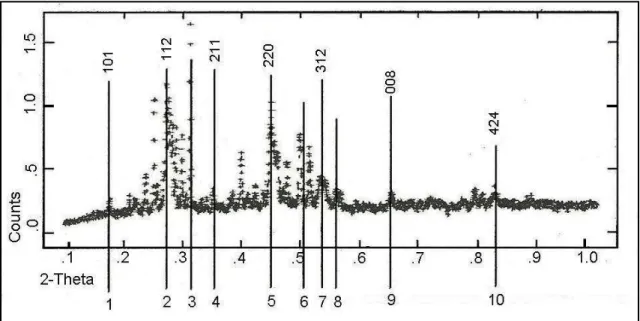
The typical measurement result of the ingot can be seen in Figure 3. By using the GSAS (General Structure Analysis System) method the miller index and crystal orientation of CuGa0.5In0.5Se2 can be discovered. The Figure shows that the crystal orientation is [101], [112], [102], [211], [213], [220], [301], [312], [008], and [424]. These crystal orientations show that crystals of CuGa0.5In0.5Se2 also possess the principal crystal orientation of solar cell material CuInSe2 and CuGaSe2, these are similar with Liao and Rockett, 2002 ; Dale et al, 2008 ; and Terasako et al 2006 [10, 3, 5] researches, Table 1 shows the relation between diffraction 2 θ angle, miller index h, k, l, and the distance inter-crystal d space.
195
Table 1. Lattice Parameter of CuGa0.5In0.5Se2 a, c and miller index d
distance inter-crystal
l. miller 2 θ
h k l
5.060 1 0 1 17.5194
3.279 1 1 2 27.1843
3.143 1 0 3 28.3848
2.487 2 1 1 36.1005
2.107 2 1 3 42.9057
2.010 2 2 0 45.0872
1.870 3 0 1 48.6724
1.711 3 1 2 53.5371
1.417 0 0 8 65.8912
1.305 3 3 2 72.3882
1.161 4 2 4 83.1773
By using data in Table 1, the lattice parameter of CuGa0.5In0.5Se2 a and c can be determined with the following formula:
1 /d2 hkl = { [ (h2+ k2 ) / a2 ] + 12 / c2 }
The result of a, c, and c/a can be seen in Table 2. It is determine that the result of c/a’s value, is that c/a≈2, and this indicates that the crystal structure of CuGa0.5In0.5Se2 is a chalcopyrite structure.
Table 2. Lattice Parameter of CuGa0.5In0.5Se2
2 θ Lattice Parameter (Ǻ)
a c c/a
17.5194 5.6595 11.2965 1.9960
27.1843 5.6804 11.3547 1.9989
36.1005 5.7005 11.3151 1.9849
45.0872 - - -
53.5371 5.6768 11.3086 1.9920
65.8912 5.8444 11.6846 1.9992
83.1773 5.6809 11.3576 1.9962
The result of characterization using XRF is shown in Table 3. Table 3 shows the % weight composition of several parts of the ingot, whereas Figure 4 shows one of the examples/typical measurement of one of the samples using XRF. Table 3 shows that the % weight composition of CuGa0.5In0.5Se2 in every part/area of division does not indicate a stoichiometric composition, only the sample of the second part indicates the best composition which is: Cu = 20.7233%, Ga = 9.1403%, In = 28.8963%, and Se = 41.2401%. This sample shows that there is an overweight of In and insufficient weight of other elements Cu, Ga, and Se. Overall, measurement with XRF is not yet sufficient, and this may be caused by in the ingot producing process where rocking process supposed to be spinning at low speed rather than swinged with 360o angle.
Table 3. % Weight Composition of CuGa0.5In0.5Se2
Samples Content wt (%)
Cu Ga In Se
1 45.7662 7.0429 9.0601 35.7528
2 20.7233 9.1403 28.8963 41.2401
3 8.1672 15.0828 48.2764 24.9801
196
Fig. 4. Typical XRF Result of one of the samples 4. ELECTRICAL CHARACTERIZATION
Electrical characterization utilizes a four-point and two-point probe: the first measurement is to measure resistivity and the second measurement is to determine the type of material. Electric characterization only uses a one-time measurement of
resistivity as well as material type measurement. First measurement shows that CuGa0.5In0.5Se2resistivity is 6.280 Ωm, whereas
the second measurement shows that material type is semiconductor p type. The resistivity shows indicates that CuGa0.5In0.5Se2 is
a semi-conductor material. Recently many device solar cell Cu(Ga x In 1-x )Se2 couple with CdS or ZnS conducted by Pudov et al.
2002, Kannan et al. 2003 , and T. Nakada and Mizutani 2002 [7, 9, 11] shown that the material Cu (Ga x In 1-x) Se2 are
semiconductor p type .
5. CONCLUSION
This research shows that CuGa0.5In0.5Se2 material is a material that has a chalcopyrite crystal structure as is the case of its derivate
CuInSe2 and CuGaSe2which has a lattice parameter of a and c/a≈2. Crystal orientation and miller index h, k, and l is also the
same as its derivate material. The composition of CuGa0.5In0.5Se2 is still not satisfactory and the ingot form is also not yet perfect
as there are still parts which are poreous. A more detailed research is required especially during the production process where rocking should be conducted by spinning the tube with a low velocity spin.
6. REFERENCES
[1]. Meeder, A., D. Fuertes Marro´ n, A. Rumberg, and M. Ch. Lux-Steiner. 2002. “Direct Measurement of Urbach Tail and Gap State Absorption in CuGaSe2Thin Films by Photothermal Deflection Spectroscopy and The Constant Photocurrent Method”. J. Appl. Phys.,
Vol. 92, No.6.
[2]. Bernède, J.C. and L. Assmann. 2000. “Polycrystalline CuInSe2Thin Films Synthesized by Microwave Irradiation”. Vacuum, Vol. 59,
No.4, pp. 885 – 893.
[3]. Dale, P J., A P Samantilleke, G Zoppi, I Forbes and L M Peter. 2008. ”Characterization of CuInSe2 Material and Devices: Comparison of
Thermal and Electrochemically Prepared Absorber Layers”. J. Phys. D: Appl. Phys. 41,085105 (8pp).
[4]. Siebentritt S., I. Beckers, T. Riemann, J. Christen, A. Hoffmann and M. Dworzak .2005. “Reconciliation Of Luminescence and Hall Measurements on The Ternary Semiconductor CuGaSe2”. Appl. Phys. Lett. 86, 091909.
[5]. Terasako, T., Y. Uno, T. Kariya and S. Shirakata. 2006. “Structural and Optical Properties of In-rich Cu-In-Se Polycrystalline Thin Films
Prepared By Chemical Spray Pyrolysis”. Sol. Energy Mater. and Sol. Cells, Vol. 90, N°3, pp. 262 – 275.
[6]. Nakada, T., and M. Mizutani. 2000. “Improved Efficiency of Cu(In,Ga)Se2 Thin Film Solar Cells with Chemically Deposited ZnS Buffer
Layers by Air Annealing Formation of Homojunction by Solid Phase Diffusion”. Proc. of the 28
th
IEEE Photovoltaic Specialists Conf., Anchorage, pp. 529-534.
[7]. Pudov, A.O., J.R. Sites, and T. Nakada. 2002 “Performance and Loss Analyses of High-Efficiency Chemical Bath Deposition (CBD)-ZnS/Cu(In1-xGax)Se2 Thin-Film Solar Cells”. Jpn. J. Appl. Phys. 41, Part 2, No 6B, L672-674.
[8]. Guillemoles. 2000. “Stability of Cu(In,Ga)Se2Solar Cells: A Thermodynamic Approach”. Thin Solid Films, 361-362, 338-345. [9]. Kannan, R., M. A. Contreras, C. L. Perkins, S. Asher, F. S. Hasoon, et al.2003. “Properties of 19.2 % efficiency ZnO/CdS/CuInGaSe2
Thin film Solar Cells”. Prog. Photovolt. Res. Appl., 11, 225-230.
[10]. Liao, D. and A. Rockett. 2002 “Effect of Surface Orientation on the Growth and Properties of Cu(In,Ga)Se2”, Proceedings of the 29
th
IEEE Photovoltaic Specialist Conference. New Orleans, USA, pp. 515
[11]. Nakada, T., and M. Mizutani. 2002. “18% Efficiency Cd-Free Cu(In, Ga)Se2 Thin-Film Solar Cells Fabricated Using Chemical Bath Deposition (CBD)-ZnS Buffer Layers”. Jpn. J. Appl. Phys. 41,Part 2, No. 2B, L165-167.