Minibands and Wannier-Stark Ladders in Semiconductor
Superlattices Studied by Infrared Spectroscopy
M. Helm, W. Hilber,
Institut fur Halbleiter- und Festkorperphysik, Universitat Linz, A-4040 Linz, Austria
G. Strasser,
Institut fur Festkorperelektronik, TU Wien, A-1040 Wien, Austria
R. DeMeester, and F. M. Peeters
Department of Physics, University of Antwerp (UIA), B-2610 Wilrijk, Belgium
Received 27 May, 1999
We review the basic features of interminiband absorption in superlattices, focussing on the joint density of states, the oscillator strength and the associated sum rule. Then we will discuss infrared spectroscopic studies under application of an electric eld. With a eld in the plane of the layers, a hot-electron distribution can be generated. Using the temperature dependence of the interminiband absorption, energy loss and relaxation rates can be determined. A vertical electric eld leads to negative dierential resistance, domain formation and the break-up of the minibands into Stark ladders. We will present experiments showing the formation of interpenetrating Wannier-Stark ladders in the continuum, which are strongly coupled by Zener resonances. This is the rst time to correlate transport and infrared absorption in a biased superlattice.
I Introduction
Semiconductor superlattices are a fascinating model system for electrons in a periodic potential [1]. They have enabled researchers to observe long-sought physi-cal phenomena such as Wannier-Stark lophysi-calization [2] and Bloch oscillations [3]. In the present paper we would like to review some of the basic properties of electrons in superlattices, in particular those related to optical transitions between minibands within the con-duction band, which can be studied by infrared spec-troscopy [4]. We will also present some recent absorp-tion studies of superlattices under applicaabsorp-tion of an electric eld, both parallel and perpendicular to the layers. Whereas in the former case information on the hot-electron relaxation is obtained [5], the latter exper-iment reveals the formation of Wannier-Stark ladders far in the continuum and allows us, for the rst time, to correlate the current-voltage characteristic with the infrared absorption spectrum [6].
II Interminiband absorption
The conduction band of a GaAs/AlGaAs superlattice (SL) can be well described using the envelope function method, which, in the case of only one band, reduces to the Kronig- Penney model with dierent eective masses in the well and barrier material. At rst we would like to discuss a superlattice consisting of 75 A wide GaAs quantum wells and 25 A wide Al0:3Ga0:7As
barriers. The calculated band structure is shown in Fig. 1. The rst miniband has a width of 1= 18 meV, the
second of 2= 70 meV approximately. If the
photodetectors", QWIPs) [8] and lasers (\quantum cas-cade lasers") [9]. In a strong- coupling superlattice, as in the present case, the thin barriers give rise to a
-nite miniband width and kz-dispersion. The absorption
coecient, , can then be written in the form [10]
c
= e2kT
0c ~
2m! Z
=d 0
dkz jh1jp
z j2ij
2
ln
1 + exp([EF ,E
1(kz)]=kT)
1 + exp([EF ,E
2(kz)]=kT)
,= (E2(kz)
,E 1(kz)
,~!) 2+ ,2
(1)
d
Here the parameters in the prefactor have their usual meaning, is the refractive index. The integration over kx and ky has already been performed
assum-ing parabolic bands, which leads to the logarithmic Fermi-Dirac factor. The energy-conserving -function has been replaced by a Lorentzian with full-width at half-maximum (FWHM) of 2,. The integral over kz
has to be evaluated numerically, using the miniband dispersions En(kz) in the Lorentzian. Note that also
the matrix elements are kz-dependent.
Figure 1. The calculated miniband structure of the GaAs/AlGaAs superlattice under investigation (well width 75 A, barrier width 25 A ). The horizontal dashed line indi-cates the top of the barriers. The 1s and 2pzimpurity states
are also included schematically [4]. The interminiband tran-sitions at the center and the edge of the mini-Brillouin zone are indicated as well as the impurity transition.
There are three essential contributions to the ab-sorption coecient: the squared momentum matrix
el-ement (which is proportional to the oscillator strength through f12 = (2=m
~
21) jh1jp
z j2ij
2), the Fermi-Dirac
thermal occupation factor, and the Lorentzian. To-gether with the kz integration the latter is nothing
less than the joint density of states (JDOS), which has two singularities at the center (kz = 0) and the edge
(kz= =d) of the mini- Brillouin zone with a 1= p
! di-vergence, characteristic of its one-dimensional charac-ter. The JDOS for transitions between the two lowest minibands of the above superlattice is shown in Fig. 2 (dotted curve). The singularities are smoothed out by a broadening parameter of , = 10 meV. The full curve in Fig. 2 reects the total absorption coecient according to eq.1 using an electron concentration of 610
17cm,3
and a temperature of T = 5 K. (At this doping level the Fermi energy lies above the top of the rst mini-band, i.e., the rst miniband is \full"). There is now a strong asymmetry with an enhanced low-frequency peak, which corresponds to transitions at the edge of the mini-Brillouinzone (near kz= =d). The reason for
this is the variation of the oscillator strength, f12(kz),
across the Brillouin zone. In our present superlattice the oscillator strength varies from f12(kz = 0) = 0.3
to f12(kz = =d) = 2.3. This can be compared to the
oscillator strength of an innite single QW, which is f12= 0:96.
Such a behavior is characteristic of most superlattice band structures (it has actually been employed in mini-band cascade lasers [11]), and is related to an extension of the well- known oscillator sum rule to periodic sys-tems with energy bands. It reads
X j
fij+ m ~
2
@2E i(kz)
@k2 z
or
X j
fij(kz) = 1 ,
m
m(i) SL
(2) m(i)
SL is the eective mass along the z-direction, which
is related to the curvature of the miniband at a cer-tain point along kz. In the above equation the rst
term describes transitions between dierent minibands (inter-miniband transitions). The second term, which is absent in atomic system and contains the curvature of the miniband at a certain point along kz, corresponds
to free-carrier type of transitions within one miniband [4]. From Eq. 2 it is clear that a large curvature (or a small eective miniband mass mz) will strongly
inu-ence the values of fij(kz). Since the minibandcurvature
is positive near kz= 0, the oscillator strength has to be
reduced there, whereas it has to be enhanced due to the negative curvature near kz= =d in order to fulll the
sum rule. Physically this corresponds to the possibility of free-carrier absorption and emission, respectively.
Figure 2. Calculated joint density of states (JDOS, dotted) and theoretical absorption coecient for the above SL with
n= 610
17 cm,3 at T=5 K.
Let us now turn to the experiment. Two GaAs/AlGaAs SLs with the above mentioned param-eters were investigated, one homogeneously doped to n = 610
17 cm,3 (having 200 periods), the other
one to n = 610
16 cm,3 (and 500 periods). A
cru-cial dierence is that in the higher-doped sample the Fermi energy (at low temperature) lies above the top of the rst miniband (which is \full"), whereas in the lower-doped sample it lies approximately in the middle of the rst miniband (it is \half-lled"). Both sam-ples were prepared in a multi-pass waveguide
geome-try with wedged facets in order to provide a nite z-component of the electric eld of the infrared radiation and thus a coupling to the interminiband transition. The measurements were performed with a rapid-scan Fourier-transform spectrometer, the samples mounted in a LHe ow-cryostat with variable temperature. The absorption spectrum of the higher-doped sample, ob-tained by ratioing p- and s-polarized transmission, is shown in Fig. 3. Evidently it agrees very well with the calculated spectrum in Fig. 2 and also does not change much with temperature. The situation is dier-ent for the lower-doped sample (Fig. 4). In this case the top-edge of the rst miniband can be populated with electrons by increasing the temperature and thus the absorption spectrum becomes strongly temperature dependent. The temperature dependence is thus a clear proof of the kz-dispersion of the rst miniband. The
ad-ditional line appearing at low temperature at~! = 125
meV is due to the 1s,2p
zdonor transition [10] and its
discussion is beyond the scope of the present paper [4].
Figure 3. Measured absorption spectrum of the higher doped SL at T=20 K and T=300 K (absorbance = -log10
(transmission)). This should be compared with the theoret-ical curve in Fig. 2.
III Hot-electron relaxation
In this section we would like to show, how the temper-ature dependence of the interminiband absorption can be used as an intrinsic thermometer for the electrons, and how the energy relaxation of the electrons can be measured [5]. When an electric eld is applied par-allel to the SL layers, the electron distribution will be heated up. If impurity and electron- electron scattering are strong enough and the eld is not too high, the re-sulting electron distribution will still be quasi-thermal, with an electron temperature T
e. Since the shape of
the absorption spectrum is mostly determined by the electron distribution, the electron temperature can be deduced by comparing the spectra at certain electric-eld values with spectra at certain lattice temperatures. Finally, the electron temperature reached in the electric eld allows one to determine the electron heating and, in steady state, cooling rate.
For the experiment the above lower-doped SL is pre-pared with two ohmic contact stripes on the sides and voltage pulses up to 38 V (electric eld F=190 V/cm) and 10 s duration are applied to them with a
repe-tition rate of the order of 100 Hz. The transmission experiment is performed using the Fourier-transform spectrometer in a gated step-scan mode, where IR spec-tra can be recorded during a short time window and the spectrometer is synchronized with the electric eld pulses. The sample is held at a lattice temperature of
T
L=10K.
Fig. 5 shows the dierential transmission spectra for dierent electric-eld values. The transmission spectra during an electric-eld pulse have been recorded and divided by a spectrum taken 10s after the pulse. For
comparison with the temperature dependent spectra, the data of Fig. 4 are replotted in Fig. 6. Here the transmission spectra at dierent temperatures are di-vided by the spectrum at T
L=10K. The striking
simi-larity between Figs. 5 and 6 indicates that the assump-tion of a quasi-thermal electron distribuassump-tion funcassump-tion is well justied. The electron temperature, T
e, at each
electric eld can now unambiguously be determined by comparing both gures, i.e., each electric-eld value in Fig. 5 can be assigned to an electron temperature.
Figure 5. Electric-eld dependence of the transmission change: The transmission spectrum at the time of the volt-age pulse is divided by the transmission after the pulse. The respective electric- eld values are indicated.
Figure 6. Ratio of the transmission at the lattice tempera-tureTL(as indicated) to the transmission atTL= 10K.
From these data the average of the power loss and energy relaxation rate of the electron system as a func-tion of electron temperature can be determined in the following way. The power loss per electron is given by
eF
2, where
is the electron mobility, taken from
tem-perature dependent mobilitymeasurements (typically a few 1000 cm2/Vs). Then an average energy relaxation
time,
e, can be determined via the balance equation eF
2
e= <(T
e)
>,<(T L)
> : (3)
Here < (T e)
> and < (T L)
> are the carrier
en-ergies averaged over the hot distribution function at an electron temperature T
e and at equilibrium (where T
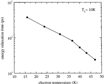
e = T
eq. (3) using the numerically calculated SL band struc-ture. The resulting energy relaxation time as a func-tion of electron temperature is shown in Fig. 7. It continuously decreases from 400 ps at 15 K to about 20 ps at 48 K. A more detailed analysis [5] shows that at low electron temperature the energy loss is governed by emission of acoustic phonons, whereas at higher tem-perature (T
e
>30 K) optical phonons, emitted by
elec-trons in the high-energy tail of the distribution func-tions, dominate the relaxation. These values can be compared with a momentum relaxation time of around 0.1 ps as deduced from the mobility,which is dominated by impurity scattering.
Figure 7. Energy relaxation time as a function of electron temperature.
IV Vertical transport and Wannier-Stark ladders
A vertical electric eld, applied perpendicular to the layers of a superlattice, is known to split up the mini-bands into a ladder of localized states, the Wannier Stark ladder (WSL). Its existence has been demon-strated through interband optical experiments, involv-ing transitions from the valence to the conduction band [2]. In a semiclassical picture, the electron can reach the inection point at the edge of the mini-Brillouin zone, giving rise to negative dierential resistance (NDR) in the current-voltage characteristics and to Bloch oscilla-tion [12,13], which is the semiclassical analogue of the Wannier-Stark ladder. Bloch oscillations have been ob-served directly in the time domain by optically exciting
electron wavepackets with a sub- picosecond laser pulse [3]. NDR, however, also arises in more weakly coupled superlattices, where transport proceeds by sequential resonant tunneling, and is usually accompanied by the formation of electric-eld domains [14,15]. In the very high-eld regime, the resonant Zener breakdown has been observed [16] as well as infrared emission from Wannier-Stark ladders [17].
The experimental methods discussed in the previous section can now be employed to study the intermini-band absorption under application of a vertical electric eld. This opens up the possibility to spectroscopically investigate the above mentioned phenomena in the in-frared domain, using transitions between electron states only. Such type of investigations have only been per-formed on isolated quantum wells (with thick barriers), showing phenomena such as Stark shifts [18] or trans-fer of oscillator strengths in coupled quantum wells [19]. On the other hand, note that transport and interband
optical experiments in a superlattice have been reported [20].
In strongly coupled superlattices, the nite mini-band width gives rise to large current densities in a vertical electric eld, which are of the order ofj 10
3
to 104 A/cm2, corresponding to vertical resistivities, V=j, below the 10
,3 cm2 range. Thus very small
mesa structures (<< 100 m diameter) would be
quired to avoid excessive inuence of parasitic series re-sistances and sample overheating. On the other hand, the minimum mesa size for infrared measurements is around 500 m. In order to get around this
prob-lem, we compromise on the sample design. We de-sign a superlattice with a rather narrow rst miniband (to keep the current density reasonably low), but a rather wide second miniband, to achieve still strong coupling of the excited states. The sample is a 300 pe-riod GaAs/Al0:29Ga0:71As superlattice with 50 A wide
quantum wells and 80 A thick barriers, sandwiched be-tweenn
+GaAs contact layers. The resulting widths of
the rst and second miniband, 1and 2, are 1.2 meV
and 30 meV, respectively. The zero-eld band structure is shown in the left inset of Fig. 8. Note that the second miniband lies in the continuum just above the barriers (right inset of Fig. 8). The superlattice is doped in the central 30 A of the barriers, giving an areal electron concentration of 2:2510
Figure 8. Interminiband transmission spectrum for zero electric eld. The insets show the absorption process in k-space and real-space, respectively. The main absorption and the high-energy shoulder, due to the singularities in the joint-density of states, are indicated by arrows.
For the IR absorption measurements, 1mm2 mesa
structures were prepared with wedged facets in order to couple the IR light to the intersubband transitions. Fig. 8 shows the zero-eld interminiband transmission spectrum of the superlattice, obtained by ratioing the p- and s-polarization. The main absorption maximum at 164 meV and the high-energy shoulder at 180 meV (both indicated by arrows) are due to the singularities of the joint density of states at k
z =
=d and k z = 0
;
respectively. This is illustrated in the left inset, which shows the three lowest minibands.
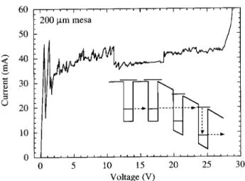
In Fig. 9 the current-voltage characteristic of a 200
m mesa is shown. At low bias the conduction is ohmic
and proceeds by ground-state to ground-state tunnel-ing up to a voltage of 0.5 V [21]. There the SL breaks up into a low- and a high-eld domain; in the latter the electrons tunnel from the ground state in one well to an excited state in a subsequent well (usually the ad-jacent well). Its extent increases with increasing bias, until the eld distribution is again homogeneous and the current rises steeply. In the present superlattice this occurs at 27 V, i.e., the voltage drop per period is 27V/300 = 90 mV. Since this is only about half the value of the subband separation,E
2 ,E
1= E
21 170
meV, we conclude that in the high-eld domain elec-trons do not tunnel to the adjacent well, but rather to the next-nearest SL period, traversing two barriers and one well (see inset of Fig. 9). This is the rst observa-tion, of resonant tunneling over two periods in a regular superlattice [22].
Figure 9. Current-voltage characteristic of the superlat-tice. The inset shows the conduction-band edge near the boundary of the low- and high-eld domain together with a schematic of the transport process.
For the measurement of the IR absorption spectrum in a vertical electric eld [6], voltage pulses of about 10
s duration with a repetition rate of a few 100 Hz were
applied to a 1 mm2superlattice mesa. The
transmis-sion change, T =T(F)=T
0, is again measured by
di-viding the signal during the electric-eld pulse,T(F),
by the signal taken a few ten s after the pulse, T 0.
Fig. 10 shows a series of traces for increasing voltage. At rst note that minima in the signal correspond to decreased transmission, i.e. they essentially correspond to absorption lines induced by the electric eld (marked by arrows). Maxima correspond to frequencies, where the absorption is reduced compared to the zero-eld spectrum. Remarkably, the positions of the maxima and minima hardly change with bias, but T
continu-ously increases, reaching up to 30% at the highest volt-age. This is completely consistent with the observations in the I-V characteristics. Two dierent electric-eld values exist in the sample, which are realized in two spatial domains; one is close to zero (in the low-eld domain), the other one (in the high-eld domain) is approximatelyF= 85mV/130 A = 65kV/cm.
Figure 10. Dierential transmission spectrum (T(F)=T0) of
the superlattice for a series of bias voltages between 8 and 30 V. Minima essentially correspond to electric-eld-induced absorption lines (marked by arrows).
Understanding the transmission change spectra of Fig. 10 requires a calculation of the absorption coe-cient, , under bias. For this purpose we have
calcu-lated the energy spectrum, the wavefunctions and the optical matrix elements between the ground state of one period and all excited states, using a nite system of N=19 SL periods. The absorption coecient is
proportional to
n(
!) = const: N X n
0 =1
f nn
0
,=
(E n
0,E n
,~!) 2
,, 2
;
(4) wherenindicates the initial state (ground state of one
SL period),n
0are the nal states, and f
nn
0is the
oscilla-tor strength, obtained from the optical matrix elements. A Lorentzian broadening ,=7 meV of each transition is assumed. The calculated absorption coecient is
plot-ted in Fig. 11 for electric elds fromF = 0 up toF= 70
kV/cm. Only up to 20kV/cm the splitting of the in-terminiband absorption into a regular Wannier-Stark ladder can be observed. At higher elds, strong mixing of several continuum Wannier-Stark ladders occurs due to Zener coupling [16,23] and the interpretation of the spectra is far from straightforward. The strong Zener coupling results from the fact that eFdis much larger
than the minigaps in the continuum.
Figure 11. Absorption coecient calculated for electric elds from 0 to 70 kV/cm. In addition, the transmission change is shown for 50, 60, and 70kV/cm in the upper panel to facilitate comparison with the experiment (see text). The experimentally relevant 60kV/cm spectra are plotted with thicker lines (compare with Fig. 10).
For direct comparison with experiment, where T =T(F)=T
0 is measured, we have to calculate the
dierence (0),(F), since
c T(F)
T(0) =
exp(,(F)d)
exp(,(0)d
exp[((0),(F))d]
for small absorption changes, as observed experi-mentally. This is plotted in the top part of Fig. 11 for F=50, 60, and 70 kV/cm. Comparison with the perimental traces, Fig. 10, shows that most of the ex-perimental features can be reasonably well reproduced for a eld of F=60kV/cm (drawn by thicker lines for clarity); only the maximumat180 meV is larger than
predicted, probably since its strength is very sensitive to the shoulder in the T0spectrum. The above eld
cor-responds to a voltage drop of 80 meV per SL period, which is very close to half the energy separation E21,
and thus conrms the tunneling to the next-nearest SL period.
In order to obtain a more graphical understanding of the transitions dominating the absorption spectrum, we attempt a classication of the energy levels in terms of pure WSL quantum numbers, neglecting the interac-tion due to Zener coupling for the moment. Then the energy spectrum can be written as
Em;p= m+ peFd; (6)
where m=1,2,... is the (zero-eld) miniband index, and p=...-1, 0, 1,...., is the spatial WSL index. Such an as-signment can be done by inspecting in detail the wave-functions and oscillator strengths over several SL pe-riods. Transitions occur from states jm = 1;p > to jm
0;p0 > and for brevity, we term such a transition
(m0;p0
,p); so, for example, (2,-1) represents a spatially
indirect transition to a WS state localized in the next downhill QW and associated to the second miniband. Fig. 12 shows the resulting assignment graphically. The main part of the relevant wavefunctions are drawn bold and also the calculated absorption coecient is shown for comparison. The main observed transitions (indi-cated by arrows) are, from low to high energies, (3,-1), (2,0) (this is the main vertical intersubband transition), (3,0), and (4,-2). Thus, besides the direct transitions, we observe indirect transitions up to the next-nearest downhill QW (p0
,p = ,2), and up to states related
to the fourth miniband (m0= 4). Note that the (4,-2)
state is as far as 200 meV above the top of the bar-rier, when measured at its associated quantum well, p0
,p =,2. The lowest- and highest-energy transitions
(at 132 and 247 meV) predicted by the calculation are not resolved in the experiment.
Figure 12. Conduction-band prole, energy levels and squared wavefunctions drawn for four superlattice periods with an electric eld of 60kV/cm. The calculation was per-formed for a 19 period SL. The experimentally observed transitions are indicated by arrows and the main parts of the respective wavefunctions are emphasized by thicker lines. The numbers on the right represent an (approximate) as-signment in terms of WS states (see text). In addition, the calculated absorption coecient is shown on the left for comparison, including the peak photon energies.
As seen in Fig. 12, the continuum WSL wavefunc-tions are distinctly dierent from the usual, symmet-rically localized tight-binding type wavefunctions [24]. They are very asymmetric and extended far towards the anode, partly exhibiting Airy-function character. Note also that due to the niteness of the structure used in the calculation, no perfect periodicity of the solution for the wavefunctions under a translation z ! z + d and
E!E,eFd is obtained. For example, (2,1) and (2,-1)
consist of two anticrossed levels, whereas (2,0) of only one level. The absorption coecient, however, which is theobservablequantity, fullls this symmetry to a much
better degree, when calculated with a nite broadening ,. In other words, the oscillator strength per nite en-ergy interval , is independent of the quantum number p, despite dierences in the wavefunctions. This shows the relation of , to the coherence length; when , is very small, the wavefunctions more easily feel the edges of the nite SL [25].
V Summary
With an electric eld applied in the SL planes, energy relaxation times can be determined by employing the temperature dependence of the absorption spectrum. Finally we have described the rst infrared absorption measurement on a biased superlattice, which has evi-denced the existence of interpenetrating Wannier-Stark ladders in the continuum of a superlattice. In the fu-ture, similar experiments extended to the far-infrared spectral region may unveil the intra-miniband[26] spec-tral response (and possibly gain) of a biased superlat-tice under Bloch-oscillation conditions.
Acknowledgment
We would like to thank A. Wacker for helpful discus-sions on superlattice transport and K. Alavi and R. N. Pathak for the growth of two samples. This work was supported by the FWF (Austria), by the GMe (Austria) and by the FWO-Vl (Belgium). R.D.M. is supported by IWT (Belgium).
References
[1] H. T. Grahn (editor), Semiconductor Superlattices
(World Scientic, Singapore, 1995).
[2] E. E. Mendez, F. Agullo-Rueda and J. M. Hong, Phys. Rev. Lett. 60, 2426 (1988); P. Voisin, J. Bleuse, C.
Bouche, S. Gaillard, C. Alibert and A. Regreny, Phys. Rev. Lett.61, 1639 (1988).
[3] K. Leo, Semicond. Sci. Technol. 13, 249 (1998) and
references therein.
[4] M. Helm, Semicond. Sci. Technol.10, 557 (1995).
[5] W. Hilber, M. Helm, K. Alavi and R. N. Pathak, Appl. Phys. Lett.69, 2528 (1996).
[6] M. Helm, W. Hilber, G. Strasser, R. DeMeester, F. M. Peeters and A. Wacker, Phys. Rev. Lett.82(1999), in
print..
[7] see, e.g. S. L. Chuang: Physics of Optoelectronic De-vices, Wiley (New York, 1995), p.373.
[8] B. F. Levine, J. Appl. Phys.74, R1 (1993).
[9] J. Faist, F. Capasso, D. L. Sivco, C. Sirtori, A. L. Hutchinson and A. Y Cho, Science264, 553 (1994).
[10] M. Helm, W. Hilber, T. Fromherz, F. M. Peeters, K. Alavi and R. N. Pathak, Phys. Rev. B48, 1601 (1993).
[11] G. Scamarcio, F. Capasso, C. Sirtori, J. Faist, A. L. Hutchinson, D. L. Sivco and A. Y. Cho, Science 276,
773 (1997).
[12] L. Esaki and R. Tsu, IBM J. Res. Dev.14, 61 (1970).
[13] A. Sibille, J. F. Palmier, M. Hadjazi, H. Wang, G. Etemadi and E. Dutisseuil, Superlattices Microstruct.
13, 247 (1993).
[14] H. T. Grahn, H. Schneider and K. von Klitzing, Phys. Rev. B41, 2890 (1990); S. H. Kwok et al., Phys. Rev.
B51, 9943 (1995).
[15] A. Wacker, in: Theory of Transport Properties of Semi-conductor Nanostructures,edited by E. Scholl (Chap-man and Hall, London, 1998), p. 321.
[16] A. Sibille, J. F. Palmier and F. Laruelle, Phys. Rev. Lett.80, 4506 (1998).
[17] G. Scamarcio, F. Capasso, A. L. Hutchinson, D. L. Sivco and A. Y. Cho, Phys. Rev. B57, R6811 (1998).
[18] A. Harwit and J. S. Harris, Jr., Appl. Phys. Lett. 50,
685 (1987); Y. Mii, R. P. G. Karunasiri, K. L. Wang, M. Chen and P. F. Yuh, Appl. Phys. Lett.56, 1986
(1990).
[19] J. Faist, F. Capasso, A. L. Hutchinson, L. N. Pfeier and K. W. West, Phys. Rev. Lett.71, 3573 (1993).
[20] A. Sibille, J. F. Palmier and F. Mollot, Appl. Phys. Lett.60, 457 (1992).
[21] Since in our sample the broadening is somewhat larger than the width of the rst miniband, we are rather in the regime of sequential resonant tunneling than of miniband conduction. See also: A. Wacker and A.-P. Jauho, Phys. Rev. Lett.80, 369 (1998).
[22] Note that tunneling over several periods has been re-cently observed in superlattices with a basis by: A. Kristensen, P. E. Lindelof, C. B. Srensen and A. Wacker, Semicond. Sci. Technol.13, 910 (1998).
[23] H. Schneider, H. T. Grahn, K. v. Klitzing and K. Ploog, Phys. Rev. Lett.65, 2720 (1990).
[24] J. Bleuse, G. Bastard and P. Voisin, Phys. Rev. Lett.
60, 220 (1988); M. Saitoh, J. Phys. C5, 914 (1972).
[25] C. Rauch, G. Strasser, K. Unterrainer, W. Boxleitner, E. Gornik and A. Wacker, Phys. Rev. Lett.81, 3495
(1998).
[26] G. Brozak, M. Helm, F. DeRosa, C. H. Perry, M. Koza, R. Bhat and S. J. Allen, Jr., Phys. Rev. Lett.64, 3163