Modeling of light-sensitive resonant-tunneling-diode devices
I. J. S. Coeˆlho and J. F. Martins-Filhoa)Grupo de Fotoˆnica, Departamento de Eletroˆnica e Sistemas, Universidade Federal de Pernambuco, 50740-530 Recife-PE, Brazil
J. M. L. Figueiredo
Departamento de Fisica da Faculdade de Cieˆncias e Tecnologia da Universidade do Algarve, 8000-062 Faro, Portugal
C. N. Ironside
Department of Electronics and Electrical Engineering, University of Glasgow, Glasgow G12 8LT, United Kingdom
共Received 5 November 2003; accepted 9 March 2004兲
We present a method to include the effects of light excitation on two different models of resonant-tunneling-diode-based devices. Our approach takes into account both photoconductive and charge accumulation effects responsible for shifting the static I – V curve when the structure is under light excitation. Computational simulations led to good agreement between the model and experimental results. © 2004 American Institute of Physics. 关DOI: 10.1063/1.1728290兴
I. INTRODUCTION
The resonant tunneling diode共RTD兲 attracts interest due to its highly nonlinear static current–voltage characteristic,1 which exhibits a range with negative differential resistance. The recent interest in applying RTDs for optical modulation,2 switching3–5 and photodetection6 – 8 has demanded efficient models to explain their behavior under light excitation. The work of Moise et al.6 has shown that the RTD integrated with a photodetector is a highly sensitive device 共10 A/W兲. For high-speed optical communication systems, the RTD in-tegrated with a photodetector could provide an inin-tegrated solution to the currently employed, hybrid arrangement of a separate photodector and transimpedance amplifier. How-ever, at this stage in its development, the RTD photodetector 共RTD-PD兲 needs to be modeled; such modeling should be able to give insight to RTD physics and, by means of widely available computer-aided design tools, to predict accurately its behavior under various operating conditions.
The models proposed by Brown et al.9 and Schulman et al.10 relate flow of carriers through the double-barrier structure 共DBS兲 to the bias conditions set across the RTD. They considered coherent and noncoherent current flowing components. Their models are Simulation Program with In-tegrated Circuits Emphasis 共SPICE兲 compatible and suitable for simulation under dark conditions only. Our purpose is to extend the physics-based model of Schulman et al. and the SPICE model of Brown et al. to include the effect of illumi-nation and to validate our model by comparing it with exist-ing data on the change of the dc current voltage curve under light excitation.
In this article, we describe a general method to include light-induced effects in physics-based models of optoelec-tronic RTDs such as RTD-PD. We take into account the pho-toconductive and charge accumulation effects close to the
DBS. These two effects have been referred to as responsible for the typical experimentally observed light-induced shift-ing of RTD dc current–voltage characteristic.3,4We calculate the contribution of the two effects and predict the device behavior under light excitation from the radiation character-istics and device parameters. Computational simulations were performed aiming to compare theoretical results from the proposed model to experimental data found in the literature.5
II. MODELING
We propose an improvement in the original models de-veloped by Brown et al. and Schulman et al. through the introduction of two terms to account for the effect of light. The original dependence of current on voltage is maintained for dark conditions. Therefore, following the formulation of Brown et al.,9we propose
I⫽C1共V⫹ReqI⫹Vph兲3兵tan⫺1关C
2共V⫹ReqI⫹Vph⫺VT兲兴
⫺tan⫺1关C
2共V⫹ReqI⫹Vph⫺VN兲兴其
⫹C3共V⫹ReqI⫹Vph兲5⫹C4共V⫹ReqI⫹Vph兲3 共1兲 and Schulman et al.,10
I⫽A ln
再
1⫹e e关B⫺C⫹n1共V⫹ReqI⫹Vph兲/kT兴 1⫹ee关B⫺C⫺n1共V⫹ReqI⫹Vph兲/kT兴冎
⫻再
2⫹tan⫺1冋
C⫺n1共V⫹ReqI⫹Vph兲 D册冎
⫹H关en2e共V⫹ReqI⫹Vph兲/kT⫺1兴, 共2兲where Vphis a photoinduced voltage共dependent on the light intensity shone on the structure兲 due to the charge accumu-lation effect, and Reqis an equivalent series resistance which accounts for the photoconductive effect and/or for the共fixed兲 resistances of the bias circuitry. The calculation of these two terms will be discussed in Sec. III. The other factors are a兲Electronic mail: jfmf@ufpe.br
8258
fitting parameters—as originally defined by the authors, C1,
C2, C3and C4共see Ref. 9兲 in Eq. 共1兲 and A, B, C, D, H, n1 and n2 共see Ref. 10兲 in Eq. 共2兲—obtained from the current– voltage curve measured under dark conditions. Therefore, the effect of light is taken into account by the Vph and Req terms only.
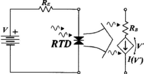
A first interpretation for Eqs. 共1兲 and 共2兲 is that they represent nonlinear voltage-controlled current sources that describe the RTD dc behavior, and are dependent on the intensity of light as illustrated in Fig. 1. Impinging photons modulate both structural layers’ resistivity and accumulated charge populations in the spacer layer共collector side兲 of the RTD.
III. ESTIMATION OF PARAMETERS A. Series resistances
Under dark conditions, the series resistance (RS) associ-ated to the layers placed between the electrodes and the DBS and due to the bias circuitry is given by
RS⫽RB⫹RE, 共3兲
where RB is the internal resistance due to the layers beside the DBS and RE is an external resistance associated to the contacts, wires and other bias circuit components 共Fig. 1 depicts the suggested dc equivalent electronic modeling兲. Such a resistance RS would be responsible for a drop in voltage from the power supply V to the voltage effectively applied across the DBS (V
⬘
). This effective applied voltage (V⬘
) drives the current I in a similar way, as empirically suggested in the Refs. 9 and 10.Under dark conditions, one expects
V
⬘
⫽V⫺RSI 共4兲to control tunneling probability through the DBS. On the other hand, absorption of impinging photons in the semicon-ductor layers surrounding the DBS leads to the variation of their resistivity. This variation can be expressed analytically as
⌬⫽共⫹⌬⫺⌬ 兲, 共5兲
where⌬is the increase in conductivity due to the photoin-duced hole-and-electron populations ␦p⫽␦n. Equation 共5兲 is obtained assuming⫹⌬⫽1/(⫹⌬) for large values of ⌬, that is, for ⌬ on the same order of. For the case in
which⌬is much smaller than, Eq.共5兲 is reduced to ⌬ ⫽⫺⌬/2. However, this is not the case for moderate lev-els of illumination. Simple calculations can be performed to verify this condition.
The decrease in resistivity given by Eq.共5兲 leads to the change in the built-in resistance RB, given by
⌬RB⫽⌬ l
A⫺共⫹⌬兲 xa
A, 共6兲
which turns Eq.共4兲 into
V
⬘
⫽V⫺共RS⫹⌬RB兲I. 共7兲In Eq. 共6兲, l and A are the total thickness and sectional area of the surrounding layers, respectively, and xa is the hole accumulation region length 共adjacent to the DBS兲, which effectively reduces the structural layer thickness from its original length l to l⫺xa.
Re-expressing Eq.共5兲 in terms of the equilibrium popu-lations p0 and n0, their respective mobilities in the material eandh, and the photoinduced carrier density␦p, we get
⌬⫽ ⫺共e⫹h兲␦p
e共en0⫹hp0兲关共en0⫹hp0兲⫹共e⫹h兲␦p兴 . 共8兲 An interesting aspect related to this expression arises for high levels of photogeneration in lightly doped spacer layers. In this case, Eq. 共8兲 revels the saturation of the decrease in resistivity on the optical laser intensity. More than this, ⌬ tends numerically to compensate the effect of the built-in resistance when (en0⫹hp0)Ⰶ(e⫹h)␦p since Eq.共8兲 becomes 关see Eqs. 共6兲 and 共7兲兴
⌬⬇⫺⫽e共 ⫺1
en0⫹hp0兲
. 共9兲
In other words, Eq.共9兲 is meaningful only at high optical powers when almost all of the applied voltage appears across the DBS and drives the tunneling probabilities, so that Eq. 共7兲 would become
V
⬘
⬵V⫺REI, 共10兲since we did not consider共up to this point兲 the electrostatic field arising due to the effect of the hole accumulation in the collector side of the DBS. Notice that it does not matter how thick xa is in Eq. 共6兲, ⌬RB will always cancel RB when the optical powers are high enough. In other words, high levels of illumination make layers behave more conductively so that a negligible drop in voltage is expected across them.
It should be clear that under dark conditions, RB distorts the dc characteristic of RTD-PD devices due to the voltage drop, as given by Eqs. 共3兲 and 共4兲. Therefore, the fitting parameters of Eqs. 共1兲 and 共2兲 evaluated under dark condi-tion are affected by this distorcondi-tion. When illuminated, the resistivity decreases, canceling the effect of RB, as given by Eqs. 共6兲–共9兲. Therefore, it is clear that Req⫽⌬RB in our model, and it is obtained from Eqs.共6兲, 共8兲, and 共9兲.
FIG. 1. Biasing circuit and the voltage-controlled current source equivalent model of the RTD-PD. REis the external resistance attributed to the
con-tacts, wires and/or bias circuitry; RB is the internal 共built-in兲 resistance
B. Photoinduced voltages
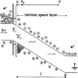
We characterize the effect of light on the current– voltage curve as an additional photoinduced drop in voltage across the DBS. The model we use to estimate the photoin-duced voltage assumes the typical RTD-PD structure, as il-lustrated in Fig. 2. Typical devices for photodetection pur-poses employ a DBS with thicker lower-doped collector-spacer layers.5,6 Their overall behavior results from modulation of the carrier’s population by the impinging pho-tons 共outer layers are made much more conductive for electrode-matching purposes兲.
As carriers are photogenerated within the surrounding areas of the DBS, excess holes accumulate beside the right side of the double barrier共see Fig. 2兲, in the collector-spacer layer. This effect is balanced by recombination and tunneling phenomena, leading to a steady excess population p close to the DBS. Such a charge distribution is responsible for two internal electrostatic fields, labeled E1and E2. As suggested earlier,9,10the voltage across the DBS drives the current be-cause it sets tunneling probability for electrons. Additional voltages, which are expected to exist there, are directly re-lated to E1 and E2.
Photogenerated charges are swept out of the thicker layer towards its boundaries due to the external biasing共see Fig. 2兲. Holes in the valence band are assumed to pile up close to the DBS uniformly spread over the interface, while photogenerated electrons are removed by the applied voltage towards the collector contact. Equilibrium in the population of holes for a certain bias voltage is sustained by a balance between arrival rate of photogenerated holes, and recombi-nation rate in the accumulation layer. There is a charge dis-tribution per unit areaS 共C/cm2兲 in a sheet whose thickness is negligible when compared to the transversal dimensions. Such a density of charges is related to the electrostatic field across the barrier layer by
D1b⫽bE1b⫽S, 共11兲
where the subscript ‘‘1’’ reminds us that this is part of the additional fields mentioned earlier.
At the interfaces between layers implementing barriers and well there are no other sheets of static charges, so that the usual boundary condition guarantees
D1w⫽wE1w⫽bE1b⫽D1b. 共12兲
Equations 共11兲 and 共12兲 allow us to estimate the total drop in voltage through the DBS due to the accumulation of holes共ifS are known兲 by
V1⫽
2wlb⫹blw
wb S
, 共13兲
where lwand lbare the thicknesses of the layers of the DBS, andw andb are their respective permittivities. Therefore, Vphin Eqs.共1兲 and 共2兲 is the V1 given by Eq.共13兲, and it is due to E1, as illustrated in Fig. 2. It can be evaluated for each optical power, upon the estimation ofS.
To estimateS, one could consider the thickness of that sheet composed of accumulated holes to set up an x-dependent electrostatic field共say E2) through the extent xa
共see Fig. 2兲. For sake of simplicity, the charge is supposed to be uniformly distributed along the thickness of this region whose volume is given by xaA, and whose hole concentra-tion is referred to as p. That means the total accumulated charge could be expressed by
Qa⫽epxaA, 共14兲
where e is the elementary charge. In addition, the electro-static field Eជ2共x兲⫽ ⫺e共xa⫺x兲p i a ˆx 共15兲
is integrated from x⫽0 to x⫽xa, giving the drop in voltage through the hole accumulation layer V2共due to E2) in Fig. 2, as
V2⫽
exa2p 2i
. 共16兲
In addition, from standard theory for semiconducting materials,11 the quasi-Fermi level shift for holes inside and outside of the hole accumulation layer allows one to write, according to the Joyce–Dixon approximation,12
V2⬵ kT e
冋
ln冉
p ␦p冊
⫹ p⫺␦p冑
8Nv册
, 共17兲where Nv is the density of states at the top of the valence band for that layer.
Equating共16兲 to 共17兲 leads to an important relation be-tween p and xa for a given bias voltage. Searching for a desirable second equation relating p to xa, it seems to be sensible, expressing a simple rate equation that neglects tun-neling holes as well as photogeneration taking place in the accumulation layer. While excess holes are being dragged to the accumulation layer from beyond xa共by the applied field兲, the rate at which they arrive can be written as
FIG. 2. Schematic diagram of the typical RTD-PD band structure共we show the bottom of the conduction band and top of the valence band as a function of distance兲 and description of the absorption, accumulation, and tunneling processes. Black circles represent thermally generated carriers, while gray circles represent photogenerated carriers.
AR⫽ vh␦p
xa
, 共18兲
where vh is the drift velocity for holes. Accumulated holes recombine at a rate given by
DR⬵ p 0
, 共19兲
where 0 is the lifetime of electron–hole pairs. We assume that for each bias voltage, AR is equal to DR, which give us the other desired equation relating p to xa.
Determining the photoinduced voltage Vph⫽V1 in Eqs. 共1兲 and 共2兲, for given conditions of illumination and biasing, depends on the task of solving the nonlinear system for p and xa, given by
再
pxa2⫽2ikT e2冋
ln冉
p ␦p冊
⫹ p⫺␦p冑
8Nv册
pxa⬵vh0␦p, 共20兲 since the calculation of p and xa leads to the calculation ofS, and therefore V1 is obtained by means of Eq. 共13兲. In summary, our model has two major components. There is a shift in the current–voltage curve to lower voltage 共i.e., the whole curve moves to the left兲 due to the reduced resistance of the epilayers surrounding the DBS caused by photoinduced carriers. This is the same effect discussed in a qualitative way by Moise et al.,6but here we have a quanti-tative model based on the entirely electrical models of Brown et al.9 and Schulman et al.10 We have also included the effect of fields induced at the accumulation layer by photoinduced holes. With this model, we are able to obtain quantitative predictions of the RTD-PD behavior.
IV. SIMULATIONS AND RESULTS
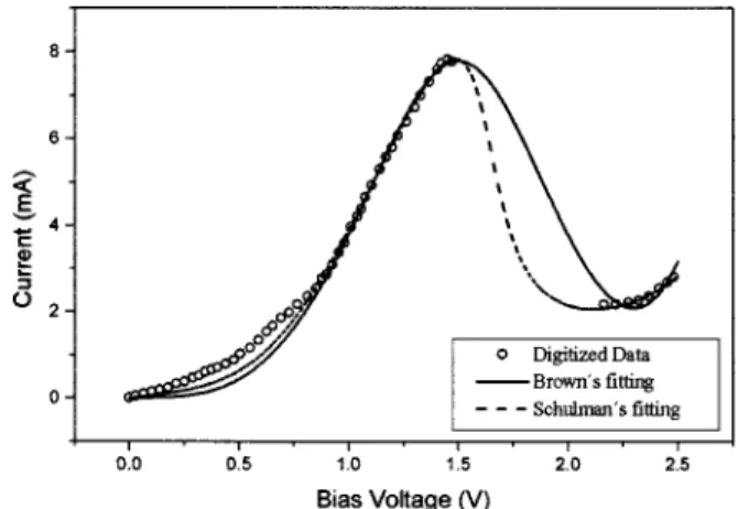
Here, we use the formulations presented in Secs. II and III to model the effect of light on the dc current–voltage curve of the RTD-PD. Different RTD structures have been reported, and discussions about which is the governing pro-cess that leads to shifting the current–voltage curve are profuse.5,6,13,14 We have chosen a particular structure in the literature for analysis, aiming to obtain simulation results for discussion.5 The choice was based on three reasons:共1兲 all features of the laser radiation as well as the structural param-eters of the RTD-PD were reported in Ref. 5;共2兲 the thicker collector-spacer layer besides the DBS is intrinsic, which is particularly suitable for our formulations; and共3兲 experimen-tal I – V curves, showing shifting for different levels of opti-cal power, are available, allowing comparisons to the ex-pected performance based on the models we have adopted and handled. Reported I – V curves in the darkness and under laser irradiation became available for analysis by picking the points up from figures of Ref. 5. The dark curve was as-sumed to express the ‘‘intrinsic curve,’’ that is, it shows the actual behavior of the RTD regardless any possible series resistances. Thus, the digitized data are fitted in Fig. 3 for initial estimation of the parameters of Eqs.共1兲 and 共2兲 under dark conditions. We removed the data in the region between the peak and the valley共the NDR region兲. Since the points in
this region were measured when the device was oscillating, they should not be considered for the dc response of the device. Therefore, our model does not take into account self-oscillation.
Next, with the fitting parameters already available, we can evaluate the effects of the laser light by estimating the voltage terms ReqI and Vph to Eqs.共1兲 and/or 共2兲.
For experimental conditions described in Ref. 5 where the intrinsic semiconducting layer exhibits Nv⫽6.4 ⫻1018 cm⫺3, for the wavelength
0⫽860 nm, the approxi-mate value for intrinsic absorption12 is ␣(InGaAs)⬃2 ⫻104 cm⫺1. We neglected optical losses due to reflections and/or absorption by free carriers in the heavily doped shal-lower layers. The estimated generation rate12 at Popt ⫽2 mW is G⬃6⫻1024cm⫺3s⫺1. Thus, the exceeding pho-togenerated population for that power is estimated to be ␦p ⫽6.5⫻1015 cm⫺3 (
0⫽1.06⫻10⫺9 s). Therefore, Eq. 共20兲 gives us the steady-state volumetric concentration of holes p⫽3.3⫻1017 cm⫺3, and the thickness of the accumulation region xa⫽21 nm. Taking these values for p and xa in Eq.
共14兲, it is possible to estimate S⫽Qa/A⬃1.1
⫻10⫺7 C cm⫺2. From Eq. 共13兲, one can obtain V 1⫽Vph ⫽119 mV, for Popt⫽2 mW.
5It is then possible to obtain the key parameter in our model, V1⫽Vph, for any optical power level. In other words, solving system共20兲 allows one to es-timate, for each optical power of the laser beam, the addi-tional voltage drop across the DBS共due to the accumulation of holes besides the inner barrier兲, which increases the tun-neling probability for electrons, left-shifting the dc character-istic of the RTD by a predetermined amount.
Accounting for the conductivity modulation of the in-trinsic layer, we assumed that there is a steady-state concen-tration of traveling electrons n0Ⰷp0under dark conditions in that material, due to tunneling/crossing-over the DBS at high enough bias voltages. Near the peak current (Ip⫽7.7 mA),5 n0⫽3.4⫻1014 cm⫺3Ⰷni⫽1.2⫻1011cm⫺3. From Eqs. 共6兲–
FIG. 3. Obtained fitting to picked data under dark conditions. This is the assumed current–voltage curve of the device 共no external resistances are assumed to be connected to or built-in the RTD兲. Circles: digitized experi-mental data共see Ref. 5兲; line: obtained fitting based on the Brown’s mod-eling (C1⫽3.44157⫻10⫺3, C2⫽1.872 04, C3⫽3.515 57⫻10⫺4, and C4
⫽⫺3.033 62⫻10⫺3are the fitting parameters兲. Dash: obtained fitting based on the Schulman’s modeling (A⫽7.46⫻10⫺4, B⫽0.130, C⫽0.2305, D ⫽0.017, H⫽2.4⫻10⫺6, n
1⫽0.141, and n2⫽0.069 are the fitting
共9兲, we concluded that in the limit of high optical power, ⌬→⫺ 共meaning that there is a reduction in the resistivity level of the semiconductor layer by an amount that is equal to the resistivity value兲 when ␦pⰇn0 ( PoptⰇ0.1 mW). Re-sistivity will depend on the current level, however, showing its higher value in the valley共7.5 ⍀ cm兲 and lower value in the peak 共1.7 ⍀ cm兲. The corresponding intrinsic resistance values are estimated as RBv⫽2.7 ⍀ and RB p⫽0.6 ⍀, respec-tively, leading to almost the same value for the ohmic drop in voltage RBvIv⫽RB pIp⫽4.5 mV. This is the maximum shift of the dc characteristic of the device due only to the photo-conductivity effect, when the device is illuminated. This con-tribution is much smaller than the hole accumulation effect estimated earlier, which is V1⫽Vph⫽119 mV, for Popt ⫽2 mW, for instance.
Theoretical curves were plotted from Eqs. 共1兲 and 共2兲, along with experimental data from Ref. 5 for different levels
of illumination in Figs. 4 –7. The calculated values for Vph and Reqfor each optical power level are: Vph⫽10.5 mV and
ReqI⫽4.5 mV for Pop⫽0.2 mW, Vph⫽36 mV and ReqI ⫽4.5 mV for Pop⫽0.6 mW, Vph⫽119 mV and ReqI ⫽4.5 mV for Pop⫽2 mW, Vph⫽290 mV and ReqI⫽4.5 mV for Pop⫽5 mW. The modeled curves show good agreement with the experimental ones in Figs. 4 to 6. In Fig. 7, we observe the agreement between theoretical and experimental curves is poorer. This can be due to tunneling of holes through the DBS, which causes a reduction of the hole con-centration in the accumulation region. Since our model does not take this effect into account, the theoretical curves over-estimate the Vphfor high optical powers.
From Figs. 4 to 7, we can conclude that the theoretical curves obtained from the Schulman-based model give a bet-ter match to the experimental results than the ones obtained from the Brown-based model. Although the original models are SPICE compatible,9,10,15,16 we implemented them in
FIG. 4. Experimental and modeled curves for RTD under illumination ( Pop⫽0.2 mW). Circles: digitized experimental data 共see Ref. 5兲. Line:
ob-tained curve based on the modified Brown’s modeling共same values for C1,
C2, C3, and C4as in dark conditions兲. Dash: obtained curve based on the
modified Schulman’s modeling共same values for A, B, C, D, H, n1, and n2
as in the dark兲. Calculated parameters for Pop⫽0.2 mW: Vph⫽10,5 mV, and
ReqI⫽4.5 mV.
FIG. 5. Experimental and modeled curves for RTD under illumination ( Pop⫽0.6 mW). Up-triangles: digitized experimental data 共see Ref. 5兲.
Line: obtained curve based on the modified Brown’s modeling共same C1,
C2, C3, and C4as in dark兲. Dash: obtained curve based on the modified
Schulman’s modeling共same A, B, C, D, H, n1, and n2as in dark兲.
Calcu-lated parameters for Pop⫽0.6 mW: Vph⫽36 mV, and ReqI⫽4.5 mV.
FIG. 6. Experimental and modeled curves for RTD under illumination ( Pop⫽2 mW). Squares: digitized experimental data 共see Ref. 5兲. Line:
ob-tained curve based on the modified Brown’s modeling共same C1, C2, C3,
and C4as in dark conditions兲. Dash: obtained curve based on the modified
Schulman’s modeling共same A, B, C, D, H, n1, and n2as in dark兲.
Calcu-lated parameters for Pop⫽2 mW: Vph⫽119 mV, and ReqI⫽4.5 mV.
FIG. 7. Experimental and modeled curves for RTD under illumination ( Pop⫽5 mW). Down-triangles: digitized experimental data 共see Ref. 5兲.
Line: obtained curve based on the modified Brown’s modeling共same C1,
C2, C3, and C4as in dark兲. Dash: obtained curve based on the modified
Schulman’s modeling共same A, B, C, D, H, n1, and n2as in dark兲.
MATHCAD™, using a differential correction method and the successive approximations method to obtain the fitting pa-rameters for the dark condition for the Brown’s and Schul-man’s models, respectively.
V. CONCLUSIONS
We presented a general method to include the effect of light on two static models for dc current–voltage character-istics of resonant-tunneling-diode-based devices. Our method takes into account the two physical processes usually discussed in the literature: photoconductivity and charge ac-cumulation effects in double-barrier RTD structures. Our model uses the same fitting parameters for the device I – V curve in dark conditions and then simulates and predicts the device’s behavior under an illumination condition. We per-formed computer simulations of our model using MATH-CAD™ with parameter estimations calculated from experi-mental data of previously published results. The current– voltage curves obtained with our model have matched the experimental data found in the literature, and also have given insights into the role of each physical process taking place in that particular device. For the RTD-PD device analyzed here, we found that the photoconductivity effect is negligible com-pared to the charge accumulation effect for optical powers above 0.6 mW.
We neglected tunneling of holes to keep the same for-malisms developed earlier in the assumed physics-based models for RTDs. Very often, only tunneling conditions for electrons are considered formally for I – V curves under dark-ness, and we kept the same assumption here. It is crucial to set accumulation conditions by the DBS sides, where the depletion of holes is assumed to be via recombination with tunneling electrons only. However, it is sensible to presume that this latter hypothesis weakens for higher optical powers. This may explain the poor agreement between our prediction and the actual device behavior for the highest laser intensity case analyzed.
Similar to previously reported modeling work, our model is based on an equivalent circuit, and it also contains adjustable parameters. However, these parameters are ob-tained in a systematic way from the dark current–voltage curves and from physics-based simple equations. We believe
it can be a useful tool for RTD based device design and circuit simulations for applications in optical switching and photodetection. Future work will include adapting the model to simulate the high-frequency characteristics of RTD-PDs.
ACKNOWLEDGMENTS
The authors would like to thank Eric Arantes and Sergio Campello, from the Photonics Group-DES-UFPE, for their help with computer programming and simulations. One of the authors 共I. J. S. C.兲 acknowledges scholarship support from the Brazilian agency CNPq.
1
J. P. Sun, G. I. Haddad, P. Mazumder, and J. N. Schulman, Proc. IEEE 86, 641共1998兲.
2J. M. L. Figueiredo, A. R. Boyd, C. R. Stanley, C. N. Ironside, S. G.
McMeekin, and A. M. P. Leite, Appl. Phys. Lett. 75, 3443共1999兲.
3P. England, J. E. Golub, L. T. Florez, and J. P. Harbison, Appl. Phys. Lett.
58, 887共1991兲.
4P. W. Park, H. Y. Chu, S. G. Han, Y. W. Choi, G. Kim, and El-Hang Lee,
Appl. Phys. Lett. 67, 1241共1995兲.
5T. S. Moise, Y.-C. Kao, L. D. Garret, and J. C. Campbell, Appl. Phys. Lett.
66, 1104共1995兲.
6
T. S. Moise, Y.-C. Kao, C. L. Goldsmith, C. L. Schow, and J. C. Campbell, IEEE Photonics Technol. Lett. 9, 803共1997兲.
7J. F. Martins-Filho, R. E. de Araujo, A. S. L. Gomes, J. M. L. Figueiredo,
C. R. Stanley, and C. N. Ironside, in Proc. IEEE LEOS 2000, 13th Annual
Meeting, Rio Grande, Puerto Rico, 2000, p. 15–16.
8
J. F. Martins-Filho, R. E. de Araujo, A. S. L. Gomes, J. R. Rios Leite, J. M. L. Figueiredo, C. R. Stanley, and C. N. Ironside, in Tech. Dig. SBMO/
IEEE MTT-S IMOC 2001—International Microwave and Optoelectronics Conference, Bele´m, PA, Brazil, 2001, p. 325–328.
9
E. R. Brown, O. B. McMahon, L. J. Mahoney, and K. M. Molvar, Elec-tron. Lett. 32, 938共1996兲.
10J. N. Schulman, H. J. De Los Santos, and D. H. Chow, IEEE Electron
Device Lett. 17, 220共1996兲.
11
R. S. Muller and T. I. Kamins, Device Electronics for Integrated Circuits, 2nd ed.共Wiley, New York, 1985兲.
12J. Singh, Semiconductor Optoelectronics, Physics and Technology 共McGraw-Hill, New York, 1995兲, p. 238ff.
13S. C. Kan, S. Wu, S. Sanders, G. Griffel, and A. Yariv, J. Appl. Phys. 69,
3384共1991兲.
14H. S. Li, L. P. Chen, Y. W. Chen, K. L. Wang, D. S. Pan, and J. M. Liu,
Appl. Phys. Lett. 65, 2999共1994兲.
15M. Bhattacharya and P. Mazumder, IEEE Trans. Comput.-Aided Des. 20,
39共2001兲.
16
T. P. E. Broekaert, B. Brar, J. P. A. Van der Wagt, A. C. Seabaugh, F. J. Morris, T. S. Moise, E. A. Beam, and G. A. Frazier, IEEE J. Solid-State Circuits 33, 1342共1998兲.