Universidade Federal de São Carlos
Center of Exact Sciences and Technology - Graduate Program in Physics
Optical and Transport properties of p-i-n GaAs/AlAs
Resonant Tunneling Diode
Iram Taj Awan
Supervisor: Prof. Dr. Yara Galvão Gobato
Co-supervisor:
Prof. Dr Maria Jose S. P. Brasil
Thesis submitted to the Postgraduate Program in Physics from Federal University of São Carlos, as a part of requirements for obtaining PhD title in Physics.
Ficha catalográfica elaborada pelo DePT da Biblioteca Comunitária/UFSCar
A964ot
Awan, Iram Taj.
Optical and transport properties of p-i-n GaAs/AlAs resonant tunneling diode / Iram Taj Awan. -- São Carlos : UFSCar, 2014.
85 f.
Tese (Doutorado) -- Universidade Federal de São Carlos, 2014.
1. Física da matéria condensada. 2. Semicondutores. 3. Propriedades óticas. 4. Diodos de tunelamento ressonante. I. Título.
I Dedicate this work to my beloved husband, Sarosh and
Similarity between me and my
sample is, we both are under
discovery.
Iram
Do not go where the path may
lead, go instead where there is
no path and leave a trail.
Acknowledgements
I am very grateful to have had the opportunity to undertake PhD research that has been enjoyable, challenging and worthwhile.
First and foremost I would like to express my sincere gratitude to my advisor Prof. Dr. Yara Galvao Gobato, who accepted me as a PhD student for her insightful guidance to my research and comprehensive support and encouragement on my thesis work. Without her help, my completion of doctoral degree is unreachable. Also I deeply appreciate my co-supervisor, Dr. Maria Jose S. P. Brasil for her help on developing my research skills, her intellectual suggestions and helpful discussions on project are worthy regarded. I am also particularly very grateful to Dr. Helder V. A. Galeti for his great support and fruitful contributions to this project.
Part of the experiments are performed at GPO (Group of Optical Properties) Lab at IFGW - UNICAMP. I also wish to express thanks to my PhD funding agency TWAS-CNPq and to the staff members and students of the GPO lab for their support and help. Special thanks to Miguel A.G. Balanta, Milton Tanabe (the lab technician) and Fernando Ikawa.
Thanks to Dr. Mohamed Henini, University of Nottingham (UK ), for providing us high quality samples used in this study.
To the fellows of UFSCar Anibal, Jaldair, Leonilson, Dr. Lara, Dr. Marcio Peron, Dr. Márcio Daldin, Vanessa, Mariana, Anne for sharing of "academic pain" together by the many collaborations and friendships founded throughout this period.
Special thanks to my husband Sarosh Farjam for giving me moral support, care and encouragement all the time during my PhD. Same I address for my elder sister Dr. Almas T. Awan as well. Special thanks to Pouya (one of my dearest friends).
Resumo
Neste trabalho, estudamos as propriedades óticas e de transporte de diodos de tunelamento ressonante de GaAs-AlAs do tipo p-i-n. Observamos duas emissões no poço quântico (QW) que foram associadas a recombinação e eletrons e buracos que tunelam no QW e que podem recombinar com os níveis confinados no QW ou com o nível de impureza aceitadora no QW. Foi observado que a intensidade relativa dessas bandas é bastante sensível a voltage aplicada. Em particular, a emissão ótica relativa a impureza mostrou ser mais eficiente na condição de voltagem que resulta em alta densidade de portadores no QW.
Estudamos também efeitos de spin nesses dispositivos na presença de altos campos magnéticos de até 15T. Observamos que polarização de spin de portadores é controlada por voltagem aplicada. Em particular, observamos que a polarização de spin apresenta fortes oscilações e variações abruptas dependendo da voltagem aplicada no dispositivo . Esse efeito foi associado a mudanças importantes de densidade de carga acumulada no QW em função da voltage aplicada. Foi também observado uma emissão fortemente dependente da voltagem na região dos contatos que foi associada a formação de uma gas bidimensional de eletrons (2DEG) com alto grau de polarização circular.
Abstract
In this thesis, we have investigated the optical and transport properties of a p-i-n GaAs-AlAs resonant tunneling diode (RTD). The possibility of controlling and significantly varying the density of carriers accumulated at different layers of this structure simply by applying an external bias makes it very useful to investigate various fundamental issues. Furthermore, the process of tunneling that critically depends on the alignment from confined energy levels and the injection of carriers that attain quasi-equilibrium distribution at distinct accumulation layers makes this structure very special for analyzing optical properties in general, and in special, spin-polarization effects when an external magnetic field is applied to the RTD.
Particularly, two emission bands were observed for the quantum well (QW) of our structure and were associated to the recombination of electrons and holes that tunnel into the QW and may recombine either as an exciton involving the fundamental states of the QW or a transition involving an acceptor state in the QW. It was also observed that the relative intensity of these emission bands strongly depend on the applied bias voltage. The optical recombination involving acceptors states becomes relatively more efficient as compared to the excitonic recombination for higher densities of electrons in the QW. This effect was discussed considering how the electron carrier density depends on the applied voltage and other effects such the capture rate of holes by the acceptors and electron and hole differences concerning mobility, effective mass and tunneling processes.
Table of Contents
Acknowledgements --- IV Abstract --- V List of Figures --- VIII
Introduction --- 1
Chapter 1- Theoretical Fundamentals --- 3
1.1 - Resonant Tunneling Diodes (RTDs) --- 3
1.2 - Simple Model for Carrier Transport in RTDs --- 6
1.3 – RTDs under Magnetic Fields --- 12
1.3.1 - Atomic model --- 12
1.3.2 - Landau Levels --- 15
Chapter 2 - Materials and Experimental Techniques --- 22
2.1 - Resonant Tunneling Diode Structure --- 22
2.2- Transport Measurements --- 24
2.3 Optical Measurements - Luminescence --- 26
2.3.1 p-i-n RTD --- 27
2.3.2 - Selection Rules for Optical Transitions in Semiconductors --- 31
2.4 - Experimental Techniques --- 33
2.4.1 Polarization-resolved Magneto Luminescence --- 33
2.4.2 Time-Resolved Photoluminescence (PLRT) --- 34
Chapter 3 - Transport and Optical Studies under zero magnetic field ---- 39
Chapter 4 - Time Resolved Photoluminescence in p-i-n RTD --- 51
Chapter 5 - Magneto-Transport and Magneto-Electroluminescence Studies in p-i-n resonant tunneling diodes --- 66
Conclusion --- 82
References --- Chapter 1 --- 20
Chapter 2 --- 38
Chapter 3 --- 50
Chapter 4 --- 65
List of Figures
Page
1 . Figure 1-1 Band structure of bulk GaAs near the center of the Brillion
Zone. 4
2 . Figure 1-2
Schematic representation of a Resonant Tunneling diode (a) and its potential profile (b) showing the bottom of the conduction band and the top of the valence band along the growth direction.
5
3 . Figure 1-3
Simplified schematic profile of the conduction band for five different applied voltages between collector and emitter (a) at V = 0 (b) V = V1 (c) V1 < V < V2 (d) V = V2. Adapted by (Mizuta, et al., 1995).
7
4 . Figure 1-4 Characteristic ideal I (V) curve for RTD illustrating a
triangular profile. 8
5 . Figure 1-5
Fermi sphere in emitter region with intersection plane shown at three different voltage conditions, applied to RTD: (a) V = V1 (b) V1 < V < V2 and (c) V = V2.
9
6 . Figure 1-6
Detail of the conduction band with 2D triangular potential well formed due to the presence of accumulation layer, case with thermalization of carriers in the states of triangular QW (2D-2D tunneling).
10
7 . Figure 1-7
(a) Fermi sphere "sliced" due to the quantization in z direction with the intersection for a given voltage. (b) I(V) Curve showing three consecutive resonances.
11
8 . Figure 1-8
In the presence of spin-orbit coupling, L and S are no longer separately preserved, they presses around the total angular momentum J.
14
9 . Figure 1-9
Representation of the Fermi sphere in reciprocal space k: (a) 3D Fermi sphere without magnetic field, (b) with 2D space quantization along the z direction without magnetic field, (c) 2D system with magnetic field, the disks are broken down into concentric circles.
16
10 . Figure 1-10
Effect of magnetic field in a 2D system. (a) Energy levels and density of states of a triangular well without magnetic field, (b) Energy levels and density of states with magnetic field (in red).
17
11 . Figure 1-11
Density of states of Landau levels with and without disorder. The disorder leads to enlargement of landau energy levels through the localization of the wave functions of carriers (localized states).
18
12 . Figure 2-1
Potential profile of a symmetric p-i-n GaAs- AlAs RTD without considering the built-in electric field due to the doped layers.
13 . Figure 2-2
Schematic diagram of a DC circuit connected to p-i-n type RTD with symmetric barriers in a 4-wire mounting, showing the ammeter, the voltage source and the layers of diode.
25
14 . Figure 2-3
Schematic potential profile of sample NU491, illustrating the transport and recombination of carriers in the structure as a function of bias (a) below flat band, (b) at flat band condition, (c) above flat band.
27
15 . Figure 2-4
Diagram of potential profile of sample NU491, illustrating the photogeneration, transport and recombination of carriers in the structure as a function of bias (a) sample is biased below flat band, (b) biased at flat band, (c) biased above flat band.
30
16 . Figure 2-5
(a) Band diagram of a GaAs QW at the center of the Brilloiun zone (b) Selection rules for optical transitions between the sublevels for a circularly polarized light in a GaAs QW, the numbers in purple indicate the relative transition intensities of both recombinations s+ and s- (Zutic, et al., 2004)
32
17 . Figure 2-6
Schematic illustration of the mounting of main
components used in CW magneto-luminescence
experiments.
34
18 . Figure 2-7 Schematic illustration of the set up of main components
used in PLRT experiments. 35
19 . Figure 2-8
(a) PL image taken at P = 15mW and T = 5K, (b) Integrated PL intensity in time versus wavelength (c) Integrated PL intensity in wavelength versus time.
36
20 . Figure 3-1 (a) I(V) characteristics curve at 5K (b) for differential
conductance dI/dV and (c) d2I/dV2 . 39
21 . Figure 3-2
Schematic band diagram of the device for (a) voltages lower than flat band condition (b) at flat band condition and (c) for voltages higher that flat band condition.
40
22 . Figure 3-3 Electroluminescence spectra of QW at 4K for different
applied voltages. 41
23 . Figure 3-4
(a) Color-coded map of EL intensity as a function of applied voltage and (b) Voltage dependence of the total QW EL integrated intensity.
43 24 . Figure 3-5 I(V) characteristics curves under light excitation at T=2K. 44
25 . Figure 3-6
Schematic band diagram of the device under light excitation for (a) voltages lower than flat band condition (b) at flat band condition and (c) for voltages higher than the flat band condition.
44
26 . Figure 3-7 (a) Color-coded map of PL intensity as function of applied
27 . Figure 3-8
(a) Color-coded map of PL intensity as function of applied voltage in the region of flat band condition for laser intensity of 60 mW.
46
28 . Figure 3-9 Typical EL emission for the contact layers for different
applied. 48
29 . Figure 3-10 Color coded map of EL intensity as function of applied
bias for the contact layers. 49
30 . Figure 4-1
I(V) characteristics curve in dark and under different pulsed laser excitation powers at 5K. The flat-band condition and tunneling resonances are indicated on the graph. The photocurrent curve can be estimated by subtracting the current with and without laser excitation. Reversed bias data range is showed under a yellow background graph.
52
31 . Figure 4-2
Integrated intensity of QW emission (a) in dark and under a 15 mW pulsed laser excitation at 5K for whole bias range. (b) Detail of emission intensity for reversed bias under pulsed laser excitation. The flat-band condition and tunneling resonances are indicated on the graph.
54
32 . Figure 4-3
(a) PLRT Images at T = 5K and P = 15mW for different voltages below the VFB. (b) PL spectra obtained by integration of entire PLRT image and (c) PL spectra integrated obtained by integration of different time window at long and short times.
56
33 . Figure 4-4
PL transient obtained by integrating the PL signal for a wavelength interval around each emission, correspond to the integrated intensity of the (a) lower energy (e1) and (b) higher energy (e2) of QW emission bands. A fitting of the PL transient was made to estimate the decay time values of each emission.
57
34 . Figure 4-5
PL characteristic time obtained by fitting the PL transient of each correspondent emission, lower energy (e1) and higher energy (e2) of QW PL bands.
58
35 . Figure 4-6
TR Images at T = 5K and P = 15mW for different voltages at V>VFB (a) in dark, where only to EL is present, and (b) with pulsed laser excitation. (c) PL spectra obtained by integration of entire TRPL image.
60
36 . Figure 4-7
(a) TR Images obtained from subtraction of TR (EL) and TR (EL+PL) at T = 5K and P = 15mW, for different voltages at V>VFB. The color scale indicate the intensity of signal after the subtraction procedure, where the blue color indicate positive values and red color indicates negative values.(b) Transients obtained by integration of entire TRPL image.
37 . Figure 4-8
(a) TR Images at T = 5K and P = 15mW for different voltages at V>VFB without (EL) and with (EL+PL) pulsed laser excitation. (b) PL transient obtained from the subtraction procedure explained in the text, by the wavelength integration for each QW emission (e1 and e2) and the correspondent exponential fitting of the transient decay.
61
38 . Figure 4-9
(a) PLTR Images at T = 5K and P = 15mW for different voltages at V>VFB obtained from images under pulsed laser excitation subtracted from images without excitation (dark), here denominated Pure PL, where the blue color scale indicate positive, and red color, negative values of intensity. (b) Some critical bias transients close to e1 resonance that present a decrease of the total luminescence (pure PL negative), here showed in green when is add a constant (y0) in order to obtain the decay time.
62
39 . Figure 4-10
PL decay time obtained by fitting the pure PL transient of each correspondent emission, lower energy (e1) and higher energy (e2) of QW PL bands, when the RTD is forward biased.
63
40 . Figure 4-11 PL transients obtained from two characteristic biases
where an abrupt variation of EL intensity is observed. 64 41 . Figure 5-1
I(V) characteristic curves for different magnetic fields at temperature T = 2K. Each IV curve is shifted 0.2mA upward.
67
42 . Figure 5-2 Polarization resolved EL spectra and taken at different
voltages for both QW and contact regions at 15T 2K. 68
43 . Figure 5-3
Color coded maps of polarization resolved EL emission due to recombination in the GaAs contact region as a function of applied bias for different values of magnetic field 8T(a, b) and 15T(d, e) at T=2K. Polarization resolved EL intensity as a function of bias (c, f).
70
44 . Figure 5-4
(a) (b) are same results of figure 5-3 (d, e) in another color-coded scale and (c) Polarization resolved EL intensity as a function of bias.
71
45 . Figure 5-5
Bias dependence of EL peak positions of contact emissions showing complex voltage dependent EL emission at contact layers under 15T at 2K.
73
46 . Figure 5-6
I(V) characteristics curve and color coded maps of polarization resolved EL emission due to recombination in QW region as a function of applied bias for different values of magnetic field 8T (a, b) and 15T (d, e) at T=2K. Polarization resolved EL intensity as a function of bias (c, f).
47 . Figure 5-7
Voltage dependence of the degree of circular polarization of EL for (a) the total QW emission and for the 2DEG-h emission under 8T 2K (b) Voltage dependence of polarization degree for the 2DEG-h emission, for the total QW emission and for recombination lines E1-A0 (red symbols) and E1-HH1 (green symbols) under 15T and 2K.
75
48 . Figure 5-8
Bias voltage dependence of (a) QW peak positions (b) QW spin splitting energy (c) 2DEG-h peak positions (d) 2DEG-h spin splitting energy under 15T and 2K.
76
49 . Figure 5-9 EL polarization resolved emission spectra from QW region
at different voltages(a), (b), (c) under B = 8T and T = 2K. 78 50 . Figure 5-10
EL polarization resolved emission spectra from QW region at different voltages (a), (b), (c), (d) under B = 15T and T = 2K.
Introduction
The control of the spin degree of freedom in addition to the charge of carriers is a major aspiration for semiconductor device development for spintronics. Long spin lifetimes and the possibility to transport spins coherently over large distances in semiconductors have motivated several studies for a new generation of microelectronic devices based on the spin degree of freedom. Several systems have been proposed for spin-based devices, including magnetic metal/semiconductor junctions, all metallic devices and all semiconductor systems (Ziese, et al.; Motsnyi, et al., 2003). Particularly, it was shown that the spin-polarization of carriers in Resonant tunneling Diodes (RTDs) can be voltage-selected, which makes this device very attractive for spintronic applications. The successful operation of semi-magnetic RTDs as a voltage-controlled electron-spin-polarized filter was first reported for structures based in II-VI semiconductor alloys with a magnetic ion (Slobodskyy, et al., 2003).
In the last years, our group has been investigating spin effects in III-V non-magnetic RTDs under high non-magnetic fields (Carvalho, et al., 2007; Dos Santos, et al., 2008; Galeti, et al., 2012). It has been shown that both the excitonic spin-splitting energy and the polarization of the QW emission from p-i-p non-magnetic RTDs under high magnetic fields present strong oscillations near resonant voltages (Carvalho, et al., 2006). It was also shown that the spin-splitting and circular polarization degree did not present a clear correlation, which implies that the spin polarization of carriers in the QW cannot be explained by a simple thermal occupation of the QW levels. Therefore, other effects such as spin-conservation along the resonant tunneling through spin-split levels and the spin-polarization of the carriers accumulated at the contact layers should also be considered in order to explain the spin-polarized emission from these devices.
Chapter 1 - Theoretical Fundamentals
In this chapter, we discuss some theoretical concepts used in our work. We present the structure of the double-barrier diode also known as the resonant tunneling diode (RTD). We discuss the fundamental physics involved on transport, optical properties and spin effects related to this structure when an external voltage is applied to the structure.
1.1 - Resonant Tunneling Diodes (RTDs):
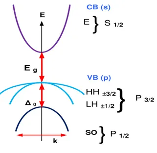
The sample studied in this thesis is a RTD composed of GaAs and AlAs layers. Both GaAs and AlAs are III-V zinc-blend semiconductors with similar lattice parameters, so that the strain developed on GaAs/AlAs heterostructures is negligible.
Figure 1-1 - Band structure of bulk GaAs near the center of the Brillion Zone. Figure modified from (Fabian, et al., 2007).
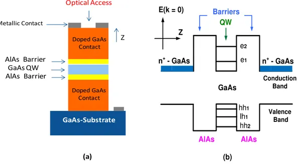
The growth of RTDs is done primarily through epitaxial growth techniques such as MBE (Molecular-Beam Epitaxy). This technique allows a controlled deposition, layer by layer, of a high-purity material. Thus, thicknesses of the components of the structure are precisely controlled. The active region of the RTD consists of a quantum well (QW) confined by two barriers connected to high-doped contact layers, known as emitter and collector. The barriers and the QW are composed of thin layers of suitable semiconductor materials with different band gap energies Eg (energy difference between the bottom of the conduction band and the top of the valence band). Figure 1-2 (a) illustrates a typical AlAs/GaAs/AlAs RTD processed as a small diode with metalized contacts. In our case, the upper contact has the form of a ring with an opened window in order to allow optical excitation and detection. Figure 1-2 (b) shows the profile of the bottom of the conduction band and top of the valence band along the growth direction of the RTD heterostructure.
E g
Δ 0
k
HH ±3/2 VB (p)
LH ±1/2
E
SO
CB (s)
}
}
P 3/2
P 1/2
S 1/2
Figure 1-2 - Schematic representation of a n-i-n Resonant Tunneling diode (a) and its potential profile (b) showing the bottom of the conduction band and the top of the valence band along the growth direction (Mizuta, et al., 1995).
The emitter and collector materials are usually made of the same material as the QW, but they are heavily doped (n or p) in order to make it possible to create ohmic contacts to the structure. Figure 1-2 (b) shows as an example a RTD where both contacts are n-type doped. In this case, we say the RTD to be a n-i-n structure. In this work we investigated a p-i-n structure that will be discussed in detail later on. In order to minimize the effects of doping impurities on the transport properties of the RTD, usually an undoped spacer-layer can be inserted between the doped emitter/collector layers and the barriers (Tsuchiya, et al., 1986). When an external voltage is applied between the RTD contacts, carriers from the doped layers are accelerated along the structure, tunneling into the quantum well, where they might remain for some time before escaping by tunneling towards the collector region or recombining with other carriers.
In ideal structures with no roughness at the interfaces that might scatter the wave-function of the carriers coupling the transverse modes with the perpendicular one, we can separate the transverse variables (x, y) from the perpendicular solution (z) for
GaAs-Substrate
AlAs Barrier GaAs QW
Z
(a)
Optical Access
AlAs Barrier
Metallic Contact
Doped GaAs Contact Doped GaAs
Contact
Conduction Band
Valence Band GaAs
AlAs AlAs
QW
Barriers
E(k = 0)
Z
hh2
n+ - GaAs e1
e2
lh1
hh1
n+ - GaAs
(b)
each of the components of the heterostructure. Thus, in a parabolic-band approximation the total energy of a carrier with isotropic effective mass m* can be expressed as:
(1.1)
The spatial localization of the wave-functions of the carriers in the QW of the RTD structure give rise to quasi-stationary states with discrete energies. Therefore, the z-component of the energy corresponds to discrete states for the conduction band ( ...) and the valence band ( , ...), which, in the context of RTD, are usually called resonant states. Notice that the quantum confinement breaks the degeneracy of the valence band top, separating the sub-bands of light- and heavy-holes. The ground-state for holes corresponds to the hh1 state as the effective mass of heavy-holes is larger than that of the light-holes.
1.2 - Simple Model for Carrier Transport in RTDs:
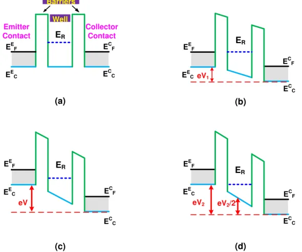
Figure 1-3 - Simplified schematic profile of the conduction band for five different applied voltages between collector and emitter (a) at V = 0 (b) V = V1 (c) V1 < V < V2 (d) V = V2. Adapted by (Mizuta, et al., 1995).
A detailed description of the transport through a RTD requires the calculation of the transmission probability T(E) for a given structure. However, we can infer some general points on the I(V) properties based on simple considerations. For T ~ 0 K, the carriers from the doped contacts occupy the states inside the Fermi sphere of radius (figure 1-5). Let´s consider in this example the tunneling of electrons, even though this model can be applied for both, electrons and holes.
EEF
EEC
ECF
ECC
(a) Well Barriers
Collector Contact Emitter
Contact ER
eV1
(b)
EEF
EEC
ECF
ECC
ER
eV2
EEF
EEC ECF
ECC
(d) ER
eV2/2
eV
(c)
EEF
EEC E
C F
ECC
Figure 1-4 -Characteristic ideal I (V) curve for RTD illustrating a triangular profile
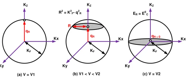
For ideal interfaces, the electrons must retain the lateral components of their momentum (kx and ky) and vertical energy component Ez. Thus, the electronic states participating in the tunneling process can be represented by the intersection of the plane = with the Fermi sphere (figure 1-5), where is the wave number associated with the resonant energy state ( ) related to energy of the bottom of the conduction band ( ):
(1.2)
As we increase the applied voltage, we vary the value of as shown in figure 1-3, thus varying the value of . Figure 1-5 illustrates three different situations corresponding to voltages defined in figure 1-3.
V1 V2
(b)
(c) (a)
(d)
NDR
Voltage (V)
C
u
rr
e
n
t
(A
Figure 1-5 - Fermi sphere in emitter region with intersection plane shown at three different voltage conditions, applied to RTD: (a) V = V1 (b) V1 < V < V2 and (c) V = V2.
The current density through the RTD should be proportional to the density of states indicated by the circle of intersection marked in grey in figure 1-5. Assuming that the tunneling probability is approximately constant for the carriers which satisfy the conditions of conservation of momentum and energy in the voltage range considered, the tunneling current density can thus be expressed as:
(1.3)
In real cases, besides the coherent tunneling described above, carriers can also perform incoherent tunneling involving impurities, interface roughness. In those cases there is no more momentum conservation along the tunneling. These processes increase the line width of the states involved, so that the I (V) curve loses its linear characteristics, the current peak becomes less abrupt and the current after the resonance does not go to zero. Furthermore, in our simple model, we assumed that electrons in both the emitter and the collector, occupy 3D–like states. This consideration no longer applies for RTD structures with undoped spacer layers adjacent to the barriers. In such case there is a voltage drop along these undoped regions, leading to formation of triangular-like potential wells (Goldman, et al., 1987), as shown in figure 1-6
qR KZ
KF
(a) V = V1 Ky
qR KZ
KF
(b) V1 < V < V2
Kx
Ky Kx
R
qR = 0
KZ
KF
(c) V = V2
Kx
Ky
(a). Due to the buildup of charge in the triangular well, these regions are called as accumulation layers.
Figure 1-6 - Detail of the conduction band with 2D triangular potential well formed due to the presence of accumulation layer, case with thermalization of carriers in the states of triangular QW (2D-2D tunneling).
The lower energy states of the triangular well correspond to localized states close to the interfaces with a quasi-2D character, while the higher-energy states are more extended and quasi-3D. Injected carriers from the doped layers by an applied voltage quickly thermalize to the lower energy states of the triangular well forming a 2D-gas. Even though those carriers eventually tunnel into the QW, they can be considered to follow a quasi-equilibrium distribution, which allows us to define a quasi-Fermi level associated with this distribution. In this condition, electrons occupy discrete energy levels along the direction perpendicular to the barriers and tunneling becomes 2D-2D (figure 1-6).
The representation of the Fermi surface in k space considering the 2D states of the triangular potential well is shown in figure 1-7. As a consequence of space quantization along the z direction, the Fermi surface is "sliced" into concentric disks along the z direction. Here again, for coherent tunneling, the lateral components of the momentum ( ) and the energy Ez must be conserved. Thus, the electronic states participating in the tunneling process are represented solely by the intersection of the plane with the discs of the Fermi surface Figure 1-7 (a). Based in this model, the I(V) curves should thus consist in a series of symmetrical narrow peaks with
Accumulation layer
QW
Emitter
Localized states
Triangular
QW Resonant
states 2D
2D
ER
intensities proportional to the areas of the disk. However, as discussed before, the real I(V) curves are broadened by scattering processes. In practice, the introduction of the undoped spacer layers results in a I(V) curve with better defined triangular-like peaks and NDR features as compared to structures without undoped spacer layers.
Figure 1-7 - (a) Fermi sphere "sliced" due to the quantization in z direction with the intersection for a given voltage. (b) I(V) Curve showing three consecutive resonances.
We remark that RTD structures allows us to select the resonant states through which the transport is performed through an applied voltage to the contacts. Therefore, if the spin degeneracy of the resonant states is broken, it opens the interesting possibility of adjusting the applied voltage so transport occurs preferentially through a level with a specific spin character, i.e. selecting the desired spin of the injected carrier. Spin degeneracy can be broken directly by applying an external magnetic field to the RTD due to the Zeeman Effect, or indirectly, through the spin-orbit coupling. The degeneracy of energy levels is directly related to the spatial symmetries experienced by the carriers. Therefore, the degeneracy of the RTD levels can be broken by an symmetry of the system, including an asymmetry of the crystal structure such as the Dresselhaus Effect (Dresselhaus, 1995) or due to the presence of intrinsic or extrinsic electric fields, such as the Bychkov - Rashba Effect (Bychkov, et al., 1984).
(b) With Scattering
0
Voltage
C
u
rr
e
n
t
Without scattering
KZ
Kx
Ky
KF
qR
Another important effect to be considered for RTDs is the spin injection from the 2D gas formed in contact region which presents high g-factors and therefore is highly spin polarized under magnetic fields. As we will discuss in the next chapters this 2D gases formed at the accumulation layers can inject spin polarized carriers into the QW.
In this work, we have performed some measurements under a high magnetic field in order to analyze spin effects on the RTD structure by using the Zeeman effect to break the spin degeneracy of the resonant states.
1.3 – RTDs under Magnetic Fields:
We now discuss in more details the effects of a magnetic field on the properties of the RTD structures.
1.3.1 - Atomic model
In order to give a physical insight of the problem, we first present a brief description of the effects of a magnetic field on a hydrogen atom, which in fact, presents certain similarities with excitons, usually related to the optical emission in semiconductor structures. Let us first consider a particle of mass and charge q =-e, without spin, submitted to a scalar potential V(R).The Hamiltonian, using the Coulomb gauge is given by:
(1.4)
Where A(R) is the vector potential associated to the magnetic field . Considering that B is uniform, the vector potential can be expressed as:
(1.5)
(1.6)
Where B is actually a constant and not an operator. Therefore all the observables commute with B, so that we can obtain:
(1.7)
Considering that:
(1.8)
We can write the total Hamiltonian of the particle as:
(1.9)
where H0, HD and Hz are defined by:
(1.10a)
(1.10b)
(1.10c)
is the Bohr Magneton (
and is the projection of R in
the plane perpendicular to B that becomes:
(1.11)
if we choose an orthogonal axis xyz where B is parallel to the z axis.
squared extension of the wave function of particle in the plane perpendicular to B (Walck, et al., 1998; Reynolds, et al., 1987). The term is called the Zeeman effect.
Let us now include the intrinsic magnetic moment of the particle (spin) simply by substituting L → L+2S in (1.14c). The factor 2 in front of S reflects the fact that the g-factor of electron in vacuum is 2. , then becomes:
(1.12)
The nature of the Zeeman effect depends critically on the magnitude of the external magnetic field compared with the actual internal field generated by the spin-orbit interaction. For , the fine structure corrections dominate and can be treated as a perturbation. In this case, the energy correction term is given in the first order of approximation, by:
(1.13)
Figure 1-8 - In the presence of spin-orbit coupling, L and S are no longer separately preserved, they presses around the total angular momentum J.
We do not know the expected values of S, but the total angular momentum
J=L+S is a constant (figure 1-8). L and S rotate around J, so that the average S is actually its projection on J:
L
S
(1.14)
But L = J - S, then and therefore,
(1.15)
Using s = 1 / 2, it follows that:
(1.16)
The term in brackets is the Lande g-factor in vacuum of an electron in an atom:
(1.17)
Thus in first order, the Zeeman term is given by:
B (1.18)
If the atom is not in vacuum, the Lande g-factor is no longer given by (1.17) and depends on the environment in which the measurements are performed, but the form of energy given by (1.18) can still be described by a similar expression.
In brief, the presence of an external magnetic field on the hydrogen atom can be described by two basic components: the diamagnetic effect and the Zeeman effect, that is responsible for breaking the spin degeneracy of the quantum states.
1.3.2 - Landau Levels (Pereira, 2001):
,
where N = 0, 1, 2, 3, ... and . The quantized states are known as the Landau levels.
Figure 1-9 - Representation of the Fermi sphere in reciprocal space k: (a) 3D Fermi sphere without magnetic field, (b) with 2D space quantization along the z direction without magnetic field, (c) 2D system with magnetic field, the disks are broken down into concentric circles.
The quantization of the motion of carriers in the direction perpendicular to the magnetic field is equivalent to an additional spatial confinement, so that in the presence of perpendicular magnetic fields, 2D systems such as a triangular QW becomes a 0D system, as shown in figure 1-9.
The Landau levels have a singular density of states (Dirac Delta function-like) with a degeneracy given by eB/m. Figure 1-10 shows the density of states and energy levels for a triangular well without magnetic field (figure 1-10 (a)) and with magnetic field (figure 1-10 (b)). Increasing magnetic fields results in an increasing degeneracy, so that the number of states that fit into each Landau level increases with B. Therefore, for sufficiently high magnetic fields, all carriers may be fallen in the first Landau level.
B
KZ
KF
(a) Ky
KZ
KF
(b)
Kx
Ky Kx
(c) KZ
KF
Kx
Ky
N0 N1
An important remark is that the energy separation all Landau levels is given by: . We point out that for a given value of the magnetic field, is inversely proportional to the effective mass (m *) of the carrier.
Figure 1-10 - Effect of magnetic field in a 2D system. (a) Energy levels and density of states of a triangular well without magnetic field, (b) Energy levels and density of states with magnetic field (in red).
Let´s now consider the effect of a magnetic field in (z) direction on the free carriers of a RTD structure. The presence of magnetic field, quantizes the lateral movement of carriers in both the emitter and the QW states. The kinetic energy of the carriers in the xy plane should then be replaced by the Landau levels, so that the energy of a resonant state shall be expressed as:
(1.19)
Once more, the components of wave-vector in the xy plane must be conserved. In this case, the Landau quantum number (N) should therefore be conserved during tunneling. Quantization into Landau levels reduces the dimensionality of the system to 0D-0D, so that the resonance peaks in the I(V) curve are symmetrical and narrow, each
ρ2D (E) z ρ (E)
(a) m*/ πћ
E
With out magnetic
field
E1
Partially filled
E
(b)
E2
EF
d= eB/h ћwC
z E1
E2
EF
relating to a given level and their different resonant Landau levels. However, as discussed before, the presence of scattering processes associated to system disorders (interfaces roughness, impurities, ...) should lead to the broadening of the Landau levels. The concept of carrier localization and Landau levels broadening into bands was first introduced by PW Anderson (Anderson, 1958), figure 1-11. In this simple view, the states in the center of the Landau bands are extended states that contributes to transport, while the states in the tails of the bands are localized and thus does not contribute to transport.
Figure 1-11 - Density of states of Landau levels with and without disorder. The disorder leads to enlargement of Landau energy levels through the localization of the wave functions of carriers (localized states).
If we now consider the spin degree of freedom from the free carriers, they should also give rise to a Zeeman-like interaction. Considering a similar approach used for the atomic case, the full expression for the energy of a free carrier in a 2D-like state can thus be expressed as:
(1.20)
C
w
E1
Extended states Localized
states
With disorder
E ρ (E)
ρ 2D
where is the cyclotron frequency , is the magnetic energy of spin, is the Lande g-factor of the effective medium and is the energy associated with movement of the carriers in z-direction.
In conclusion, the application of an external magnetic field affect the states of the carriers that accumulate as 2D gases at the QW and the accumulation layers of a RTD structure, giving rise to a series of Landau levels. This phenomenon was clearly observed in systems which have electronic transport (Goodings, et al., 1994). In the case of holes, the experimental results are not so evident due to their relatively larger effective masses, so that Landau levels for holes are usually less resolved
References
Anderson, P W. "Absence of Diffusion in Certain Random Lattices." Phys. Rev. 109.1492 (1958).
Bychkov, Yu A and E I Rashba. "Oscillatory effects and the magnetic susceptibility of carriers in inversion layers." J. Phys. C: Solid State Phys. 17.6039 (1984).
Carvalho, H B de, et al. "Voltage controlled hole spin injection in non mangentic GaAs,AlAs RTD." Physical Review B 73 (2006).
Carvalho, H B, et al. "Circular polarization from a non magnetic p-i-n resonant tunnelling diode." Applied Physics Letters 90.062120 (2007).
Dos Santos, L F, et al. "Polarization resolved luminescence in asymmetric n-type GaAs/AlGaAs." Appl. Phys. Lett. 92 (2008).
Dresselhaus, G. "Spin-Orbit Coupling Effects in Zinc Blende Structures." Phys. Rev. 100 (1995).
Fabian, Jaroslav, et al. "SEMICONDUCTOR SPINTRONICS." 2007.
Galeti, H V A, et al. "Magneto-optical investigation of two-dimensional gases in n-type resonant tunneling diodes." Semiconduc. Sci. Technol 27 (2012). <stacks.iop.org/SST/27/015018>.
Goldman, V J, D C Tsui and J E Cunningham. "Observation of intrinsic bistability in resonant tunneling structures." Phys. Rev. Lett 58 (1987).
Goodings, C J, H Mizuta and J R. A Cleaver. "Electrical studies of charge build‐up and
phonon‐assisted tunneling in double‐barrier materials with very thick spacer layers." J. Appl.
Phys. 75.363 (1994).
Mizuta, Hiroshi and Tomonori Tanoue. the physics and applications of resonant tunnelling diodes. Cambridge university press, 1995.
Motsnyi, V F, et al. "Optical investigation of electrical spin injection into semiconductors." Phys. Rev. B 68 (2003).
Pereira, Ana Luiza Cardoso. Levitações de Estados Estendidos em Sistemas que Apresentam Efeito. 2001.
Reynolds, D C, et al. "Magneto-optical studies of GaAs-As multi-quantum-well structures grown by molecular-beam epitaxy." Phys. Rev. B 35 (1987).
Tsuchiya, Masahiro and Hiroyuki Sakaki. "Dependence of resonant tunneling current on well widths in AlAs/GaAs/AlAs double barrier diode structures." Appl. Phys. Lett. 49 (1986).
Walck, S N and L T Reinecke. "Exciton diamagnetic shift in semiconductor nanostructures." Phys. Rev. B 57.9088 (1998).
Chapter 2 - Materials and Experimental Techniques
In this chapter we will briefly present the sample as well as the experimental techniques and methodologies used during our studies.
2.1 - Resonant Tunneling Diode Structure
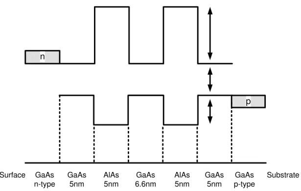
This work is based on the study of a resonant tunneling diode (RTD) composed of III-V semiconductor materials with layers of GaAs and AlAs. An undoped quantum-well (QW) of GaAs with thin barriers of AlAs is grown around GaAs n- and p-type doped contacts. This structure is usually known as GaAs/AlAs a p-i-n RTD. The sample was432
grown by Prof. Mohamed Henini from the University of Nottingham (UK), using the ||| Molecular Beam Epitaxy (MBE) technique within a scientific collaboration with his group. Using this technique, it is possible to grow crystalline layers of semiconductor materials with excellent control of thicknesses and impurity concentrations and therefore obtain heterostructures of high crystalline quality, which is reflected by their optical and transport properties. The layers of GaAs and AlAs were deposited on a (100) substrate of GaAs. The impurities used for doping the GaAs contact layers were Be and Si , for acceptors (p-type) and donors (n-type), respectively. The layers that compose the sample from top to bottom (substrate) are detailed in table 2.1 below.
layers of GaAs, adjacent to the barriers of AlAs are required to reduce the diffusion of carriers from the doped contacts into the QW (Fabian, et al., 2007; Tsuchiya, et al., 1985; Shewchuk, et al., 1985). The structure was processed on 400µm diameter mesas with a 20 µm thick top metallic contact with the shape of a ring in order to allow optical access to the structure while applying an external voltage. The other metallic contact was made in layer at the p-type GaAs layer and is thus called the bottom contact.
Material Layer size Dopant Sample region
GaAs 25nm n =
Superior Contact Region
1µm n =
GaAs 51nm n =
GaAs 35nm n =
GaAs 7.6nm Undoped Space layer
AlAs 5nm Undoped Barrier
GaAs 6 nm Undoped QW
AlAs 5nm Undoped Barrier
GaAs 5nm Undoped Space layer
GaAs 100nm p =
Inferior Contact Region
GaAs 100nm p =
GaAs 3µm p =
GaAs Substrate n-type,
Figure 2-1 - Potential profile of a symmetric p-i-n GaAs- AlAs RTD without considering the built-in electric field due to the doped layers.
2.2 - Transport Measurements
The current-voltage characteristic curves I(V) are usually used to characterize electronic devices such as RTDs. In the case of an RTD as studied here, we do not expect a linear relationship between current and voltage. In fact, the I(V) function for a RTD structure is characterized by peaks that arise at certain voltages due to resonant tunneling through confined states in the QW. The confined states through which the carriers can efficiently tunnel the double-barrier structure at certain voltages are called the resonant voltages.
To measure the I(V) curves, the structure was connected to a DC circuit (figure 2-2) that makes it possible to apply an external voltage between the top and the bottom RTD contacts and read the current flowing through the diode. In this work, we have used a voltage source (Yokogawa - Model 7651 Programmable Voltage Source) and an multimeter (Keithley - Model 197A Auto ranging Multimeter DMM) operated remotely through an acquisition software. During measurements, the sample was kept within a
p n
AlAs 5nm
GaAs 6.6nm
AlAs 5nm
GaAs 5nm GaAs
5nm
Substrate Surface GaAs
n-type
Helium super-fluid immersion cryostat at a temperature of 2 K. Figure 2-2 shows the layout of the circuit connected to the RTD.
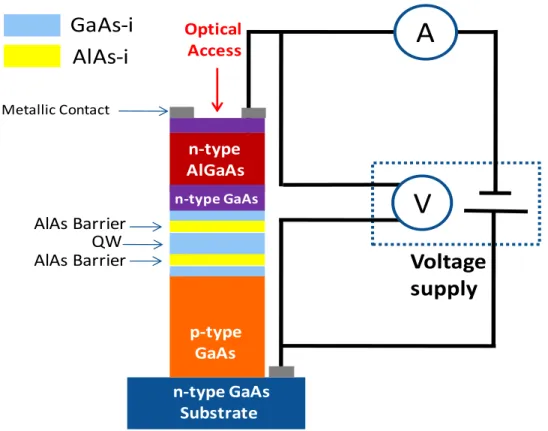
Figure 2-2 - Schematic diagram of a DC circuit connected to p-i-n type RTD with symmetric barriers in a 4-wire mounting, showing the ammeter, the voltage source and the layers of diode.
Since the sample is a p-i-n type RTD, resonances of both, holes and electrons can be observed in the I(V) curves by the procedure described above when the diode is forward biased. Resonant states can be clearly observed in the I (V) curves. In all experiments, we applied a positive voltage to the bottom contact relative to the top contact, which is called a positive bias in our convention. This kind of bias acts as to accelerate the majority charge carriers (electrons/holes) from the upper/bottom contact through the QW, which is conventionally known in the literature as a forward bias voltage. In this work, we have also studied the photocurrent by measuring the I(V) characteristics curves in dark and under light excitation.
n-type GaAs Substrate
GaAs-i
AlAs-i
A
Voltage
supply
AlAs BarrierQW
p-type GaAs n-type AlGaAs
Metallic Contact
V
AlAs Barrier
Optical Access
2.3 - Optical Measurements - Luminescence:
Although various aspects of RTDs can be observed by transport measurements, the optical study allows further exploration of the transport properties and the interactions between different carriers. We briefly discuss the physical phenomena related to the optical measurements performed in our RTD structure, including photoluminescence and electroluminescence. Both phenomena have their origin in the recombination of an electron and hole, but the way these carriers are generated, distinguish these two process.
In the fundamental state of an undoped semiconductor at T= 0 K, the conduction band is completely empty of electrons and the valence band is completely filled with electrons. If this semiconductor illuminated with light of appropriated energy, it can promote an electron from the valence band to the conduction band, leaving a hole in the valence band. For this to occur, the photon must have an energy equal or greater than the energy difference between the bottom of the conduction band and the top of the valence band ( ), where " " is the band gap. In the conduction/valence band, this electron/hole quickly relaxes to the bottom/top of the band, which is normally called the thermalization process. Thereafter, the electron can recombine with the hole left in the valence band by emitting a photon, that is called the luminescence. In this case, the pairs of electrons and holes that recombine emitting luminescence were generated by an optical excitation. Therefore, we call this luminescence as photoluminescence (PL).
Let us now discuss the processes described above for the specific case of a p-i-n RTD. To represent the dynamics of the carriers, we will use schematic band diagrams. In these representations we will use the signal convention for the applied bias as a voltage applied to
the
lower contact (close to the substrate) relative to the upper contact, as discussed before. Furthermore, we will always draw the top contact to the left and the bottom contact to the right of the figure.2.3.1- p-i-n RTD
The different doping of the contacts in a p-i-n RTD introduces an intrinsic electric field in the structure that bends the conduction and valence bands even without an external voltage applied to the RTD. Consider first the case where the voltage is applied to the RTD without illumination.
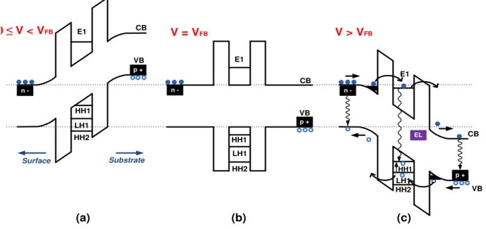
Figure 2-3 - Schematic potential profile of sample NU491, illustrating the transport and recombination of carriers in the structure as a function of bias (a) below flat band, (b) at flat band condition, (c) above flat band.
Figure 2-3 illustrates the dynamics of carriers as a function of voltage, using the convention defined above. Figure 2-3 (a) shows the intrinsic internal electric field which
CB
VB
0 ≤ V < VFB
Surface Substrate
(a)
E1
HH2 LH1 HH1
p +
n
-CB
VB E1
HH2 LH1 HH1 V = VFB
(b)
p +
n - n
-(c)
CB
HH2 LH1
HH1
V > VFB
p +
E1
VB
opposes the flow of electrons and holes towards the QW, resulting in a zero EL signal. Figure 2-3 (b) represents the RTD under an positive voltage (forward biased), so that the intrinsic field is exactly compensated by the external bias, resulting in a flat band condition. In this situation, it is still not possible to observe electroluminescence.
In the case of Figure 2-3 (c), the electrons present in the upper contact are at a higher electric potential, and therefore, are driven by the electric field towards the QW. In the same way, the holes are driven from the top contact towards the QW. Driven electrons and holes tend to accumulate at the undoped layers close to the barriers at what is called accumulation layers, forming two-dimensional (2D) gases. Carriers from the accumulation layers may tunnel into the quantum well. As we discussed in previous chapter, tunneling into the well may include two types of tunneling limits: ballistic (3D-2D) or through the accumulation layer (2D-(3D-2D). Inside the well, we emphasize on the possible processes: injected carriers on excited QW levels can relax to fundamental levels, (as shown by the transition in figure 2.3 (c), experience radiative recombination, emitting photons (EL), and tunnel out of the well through the second barrier contributing to the current through the RTD. Furthermore, carriers tunneling through the second barrier can still recombine at the GaAs contacts with opposite majority carrier.
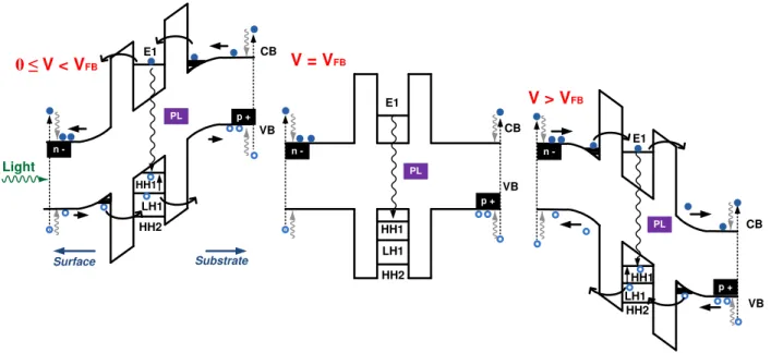
In case of figure 2-4(a) the device is forward biased below flat band (reverse biased). In this bias range, photogenerated holes at the n-type contact of the sample may recombine at this layer or be accelerated towards the p-contact, while photogenerated electrons at the p-type contact can also recombine at this layer or be accelerate towards the n-contact. Therefore, the minority carriers photogenerated at each contact layer tend to accumulate close to the barriers, from where they may tunnel into the QW. However, under this condition the majority carriers do not contribute to the current and they are not injected into the QW.
Once again, injected photogenerated carriers can relax to fundamental energy levels and experience radiative recombination, emitting photons (PL), or tunnel out of the well through the second barrier, thus contributing to the current through the RTD. Finally, photo created carriers tunneling through the second barrier can also recombine at the contacts with the opposite majority carriers in each contact.
Figure 2-4 - Diagram of potential profile of sample NU491, illustrating the photogeneration, transport and recombination of carriers in the structure as a function of bias (a) sample is biased below flat band, (b) biased at flat band, (c) biased above flat band.
For voltages greater than 1.5V, the device is forward biased beyond flat band as shown in figure 2-4 (c). In this situation, both intrinsic and photogenerated electrons in the upper contact and intrinsic and photogenerated carriers from the bottom contact are pushed against the QW and tend to accumulate generating 2D gases next to the AlAs barriers. These carriers tunnel into the quantum well, where they can relax to the fundamental energy levels and recombine emitting a EL+PL signal or tunnel out of the QW, contributing to the current through the RTD. Once more, the carriers that traverse the double barrier can also recombine at the contacts, emitting a luminescence signal.
For all three cases discussed above, we applied a positive voltage to the substrate relative to the top contact. When a negative voltage is applied to the substrate, the RTD is even further reverse biased.
In this work, we investigated the PL and EL emission as a function of the applied bias, including time-resolved PL and EL measurements under high magnetic fields. We observe that under a magnetic field, the spin degeneracy of the resonant states of the localized states at the triangular wells and inside the QW are broken. On those measurements, we analyzed the circular polarization of the luminescence, that gives
n
-CB
HH2 LH1 HH1 V > VFB
p +
E1
VB
PL
CB E1
HH2 LH1 HH1
VB V = VFB
p + n
-PL
CB
VB
Light
E1
HH2 LH1
HH1
p +
n
-PL
Surface Substrate
information on the spin polarization of the carriers involved on each recombination band.
2.3.2 - Selection Rules for Optical Transitions in Semiconductors
Optical transition, including absorption and recombination, must obey the fundamental laws of energy and angular momentum conservation. Photons of right or left polarized light have a projection of the angular momentum on the direction of their propagation equal to +1 or −1, respectively (in units of ħ). When a circularly polarized photon is absorbed, this angular momentum must be distributed between the photo-excited electron and hole according to the selection rules determined by the band structure of the semiconductor. Although the complex nature of the semiconductor bands, the momentum conservation result is equivalent to optical transitions between atomic states with j = 3/2, mj = −3/2, −1/2, +1/2, +3/2 (valence bands of light- and heavy-holes) and j = 1/2, mj = −1/2, +1/2 (conduction band).
Possible transitions between these bands, as well as those involving the split-off (SO), for a zinc-blende bulk semiconductor such as GaAs are represented in figure 2.5. Optical absorption/emission occurs for electron-hole pairs or its bounded state (excitons) in such a way that:
+ = = ,
Figure 2-5 - (a) Band diagram of a GaAs QW at the center of the Brilloiun zone (b) Selection rules for optical transitions between the sublevels for a circularly polarized light in a GaAs QW, the numbers in purple indicate the relative transition intensities of both recombinations + and - (Zutic, et al., 2004)
In the case of the a quantum well, the confinement of holes with different effective masses results in the splitting of light- and heavy- holes sub-bands, as shown in figure 2-5 (a). Therefore, by selecting the energy and the circular polarization of the excitation/emission from a QW it is possible to select the transition of carriers with a specific composition of angular momenta, i.e., spin polarization. We remark that in our case, even when the holes are injected into excited states, the recombination always occur through the recombination of the fundamental e1-hh1 states. (Miller).
The circular degree of polarization of the luminescence is thus defined as:
(2.1)
where and are the intensities of left and right circularly-polarized light, respectively.
E g
Δ 0
k
HH ±3/2 VB (p)
LH ±1/2
E
SO
CB (s)
}
}
P 3/2
P 1/2
S 1/2
E
}
(a)
- 1/2 1/2
3/2
1/2 - 1/2
- 3/2
CB
HH
+
+
-
-31 1
3
(b)
LH HH
LH
2.4 - Experimental Techniques
The main techniques used to investigate our RTD system in this thesis was the luminescence, including photo (PL) and electro (EL) luminescence, with the possibility of the application of an external magnetic field (magneto-luminescence) and time-resolved measurements (PL-RT). Two excitation sources for PL were used in our experiments. For measurements of magneto-PL, continuous-wave excitation (CW) by means of a solid-state laser with emission at 532 nm (Nd: YAG - Laser line) was used. For pulsed excitation, in PLRT measurements, we have used a titanium-sapphire laser (Spectra Physics - Tsunami Model).
2.4.1 - Polarization-resolved Magneto Luminescence
The CW EL and PL were performed in the laboratory of transport and luminescence of the Department of Physics at UFSCar. The experimental setup is sketched in Figure 2-6. In all CW measurements, the luminescence signal was collected by a convergent lens and focused into a monochromator, which was coupled to a Si CCD (Andor) detector.
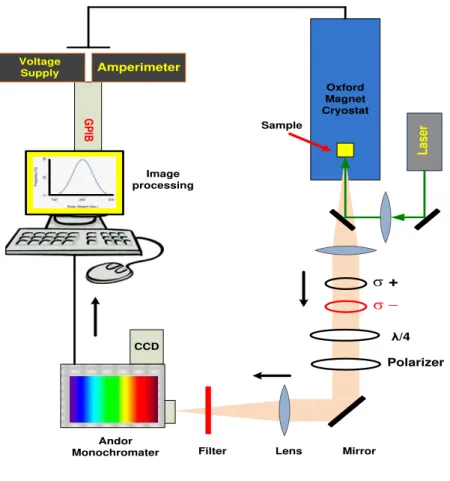
The sample was placed inside a superconducting magneto cryostat (Oxford Instruments) for measurements under different magnetic fields. The magnet reaches fields up to 15T and temperatures ranging from 2 to 300K. The cryostat has windows that allows optical excitation and collection of luminescence, and provides electrical contacts for the RTD structures. For EL measurements, a bias voltage was supplied by a programmable Voltage Source (Yokogawa - Model 7651. The optical emission was analyzed by using a λ/4 retarder (Thorlabs), and a linear polarizer (Newport) to separate
Figure 2-6 - Schematic illustration of the mounting of main components used in CW magneto-luminescence experiments.
2.4.2 - Time-Resolved Photoluminescence (TR-PL)
TR-PL measurements were performed in the Group of Optical Properties (GPO) at the Institute of Physics “Gleb Watagin” (IFGW) UNICAMP, in collaboration with Prof. Dr. Maria José Pompeu Santos Brasil using a system based in a Streak-Camera (Hamamatsu) and a Ti-Sa pulsed laser pumped by a 10 W solid-state Millenia laser (Spectra Physics). The Ti:Sa laser was tuned at 810 nm and doubled using a LiO2 non-linear crystal in order to obtain a higher excitation energy ( 405 nm). The laser pulse has a frequency of 82 MHz and temporal width of about 3 ps. The estimated time between two consecutive pulses is thus of ~ 12 ns, which is therefore the maximum time window to analyze a PL transient for this system. A home-made autocorrelator, provided a qualitative view of the laser pulse during measurements,
Oxford Magnet Cryostat
CCD
Amperimeter
L
as
er
Voltage Supply
G
PI
B
+
-λ/4
Polarizer
Lens
Filter Mirror
Sample
Image processing
The sample was placed in a He immersion cryostat and measurements were performed at ~10 K under He gas. The cryostat has quartz windows used to illuminate the sample with the laser beam and collect the luminescence.
Figure 2-7 - Schematic illustration of the set up of main components used in PLRT experiments.
Linearly-polarized beam was used, which does not favor any selectivity of spin from the photogenerated carrier. The luminescence emitted by the RTD was collected by an assembly of quartz lens and focused on the spectrometer coupled to the streak-camera fast detector system. We have used a diffraction grating with 300 lines per mm. The layout of the experimental assembly of TRPL measurements performed in the laboratory of GPO is represented in Figure 2-7. Note in this illustration a beam-splitter is placed in the path of incident laser beam between the laser Ti: Sa and the cryostat. In
Amperimeter Voltage
Supply
Sample
Beam Splitter Monochromater
Streak Camera
Autocorrelator Cryostat
Ti:Sa Laser
Ar Laser (Millenia Pro)
Pulse laser source mirror
Band Pass Filter
Lens
Photodetector
Oscilloscope
Polychromator
Delay Unit Image processing
G
PI
B
CCD