UNCORRECTED PROOF
1 2 3 4 5 6 7 8 9 10 11 12 13 14 15 16 17 18 19 20 21 22 23 24 25 26 27 28 29 30 31 32 33 34 35 36 37 38 39 40 41 42 43 44 45 46 47 48 49 50 51 52 53 54 55 56 57 58 59 1 2 3 4 5 6 7 8 9 10 11 12 13 14 15 16 17 18 19 20 21 22 23 24 25 26 27 28 29 30 31 32 33 34 35 36 37 38 39 40 41 42 43 44 45 46 47 48 49 50 51 52 53 54 55 56 57 58 59 Flexible zinc-tin oxide (ZTO) thin-film transistors (TFTs) processed at only 180 °C are reported for the first time. Although no critical elements as In and Ga are used, device performance ap-proaches the one of indium-gallium-zinc oxide TFTs. Hydrogen incorporation dur-ing ZTO sputterdur-ing and integration with a high-κ multilayer dielectric are explored to obtain Von ≈ 0 V, µFE≈ 5 cm2 V-1 s-1, and S = 0.26 V dec-1. Inverters with rail-to-rail operation (VDD = 5 V) and a dif-ferential amplifier with positive feedback loop with gain of 17 dB and unity gainfre-quency of 40 kHz are demonstrated. Q3 C. Fernandes, A. Santa, Â. Santos,
P. Bahubalindruni, J. Deuermeier, R. Martins, E. Fortunato,
P. Barquinha* ... 1800032 A Sustainable Approach to Flexible Electronics with Zinc-Tin Oxide Thin-Film Transistors
UNCORRECTED PROOF
1 2 3 4 5 6 7 8 9 10 11 12 13 14 15 16 17 18 19 20 21 22 23 24 25 26 27 28 29 30 31 32 33 34 35 36 37 38 39 40 41 42 43 44 45 46 47 48 49 50 51 52 53 54 55 56 57 58 59 1 2 3 4 5 6 7 8 9 10 11 12 13 14 15 16 17 18 19 20 21 22 23 24 25 26 27 28 29 30 31 32 33 34 35 36 37 38 39 40 41 42 43 44 45 46 47 48 49 50 51 52 53 54 55 56 57 58 59Full paper
www.advelectronicmat.deA Sustainable Approach to Flexible Electronics
with Zinc-Tin Oxide Thin-Film Transistors
Cristina
Fernandes
,
Ana
Santa
,
Ângelo
Santos
,
Pydi
Bahubalindruni
,
Jonas
Deuermeier
,
Rodrigo
Martins
,
Elvira
Fortunato
, and
Pedro
Barquinha
*
Q1
DOI: 10.1002/aelm.201800032
display backplanes and creating multi-functional flexible circuitry with thin-film technologies are considered. Within this scenario, amorphous oxide semiconductor (AOS) became one of the most competi-tive TFT technologies, enabling excellent uniformity in large areas, high transpar-ency in visible spectrum, and field-effect mobility (µFE) exceeding 10 cm2 V-1 s-1 even when fabricated below 200 °C.[1–3] The potential of these materials as semi-conductors in TFTs started to be recog-nized in 2004 with the work by Nomura et al. on flexible indium-gallium-zinc oxide (IGZO) transistors.[4]
Despite the establishment of IGZO TFTs as a key technology for large-area electronics, indium and gallium are critical raw materials, imposing impor-tant constrains regarding the sustain-ability of this approach.[5] Therefore, the ideal route for the next-generation AOS-based transistor technology should comprise an indium- and gallium-free semiconductor material, providing at least comparable performance and pro-cessing temperature to IGZO. Zinc-tin oxide (ZTO) has been recognized as a likely choice. Chiang et al.[6] reported in 2005 the first successful integration of sputtered ZTO as semicon-ductor layer in TFTs. Their staggered bottom-gate, top contact devices showed µFE≈ 20–50 cm2 V-1 s-1, turn-on voltage (Von) between -5 and 5 V, and on/off ratio > 107 when annealed at 600 °C. However, µFE drastically decreased to 5–15 cm2 V-1 s-1 when lower annealing temperature (300 °C) was used, which is still too high for temperature-sensitive polymeric substrates as polyethylene naphthalene (PEN). Since then more than 150 articles on ZTO TFTs have been published, following both physical and solution-processing routes. Focusing on sput-tering, which is the processing technique with easier penetra-tion on an industrial TFT baseline process, aspects as different Zn:Sn ratios,[7–9] chamber pressure, oxygen flow ratio, and RF power during sputtering have been studied.[10] Nonetheless, for all these experiments a processing or post-processing tem-perature exceeding 300 °C was always used to achieve proper device operation (e.g., µFE> 5 cm2 V-1 s-1 in devices properly patterned, where overestimation of mobility due to fringing effects can be neglected.[11] A very recent work by Han et al.[12] is the exception to this, where a remarkable saturation mobility (µsat) of 67 cm2 V-1 s-1 is achieved for polycrystalline tin-doped
Zinc-tin oxide (ZTO) is widely invoked as a promising indium and gallium-free alternative for amorphous oxide semiconductor based thin-film transis-tors (TFTs). The main bottleneck of this semiconductor material compared to mainstream indium-gallium-zinc oxide (IGZO) is centered in the larger processing temperatures required to achieve acceptable performance (>300 °C), not compatible with low-cost flexible substrates. This work reports for the first time flexible amorphous-ZTO TFTs processed at a maximum temperature of 180 °C. Different aspects are explored to obtain performance levels comparable to IGZO devices at these low processing temperatures, such as hydrogen incorporation during ZTO sputtering and integration with a high-κ multilayer/multicomponent dielectric. Close-to-zero turn-on voltage, field-effect mobility ≈5 cm2 V−1 s−1, and subthreshold slope of 0.26 V dec−1 are obtained. Stability under negative-bias-illumination stress is dramatically improved with hydrogen incorporation in ZTO and device performance is insensitive to bending under a radius of curvature of 15 mm. Inverters using the ZTO TFTs enable rail-to-rail operation with VDD as low as 5 V, while a dif-ferential amplifier with positive feedback loop provides a gain of 17 dB and unity gain frequency of 40 kHz, limited by the large to-source and gate-to-drain overlaps used herein.
C. Fernandes, A. Santa, Â. Santos, Dr. J. Deuermeier, Prof. R. Martins, Prof. E. Fortunato, Prof. P. Barquinha
Department of Materials Science Faculty of Sciences and Technology
Universidade NOVA de Lisboa and CEMOP/UNINOVA Campus de Caparica, 2829-516 Caparica, Portugal E-mail: [email protected]
Prof. P. Bahubalindruni Okhla Industrial Estate
Phase III, New Delhi 110020, India
The ORCID identification number(s) for the author(s) of this article can be found under https://doi.org/10.1002/aelm.201800032.
Q2
In-Free Flexible Oxide Electronics
1. Introduction
Over the last four decades displays have been the main driving force behind the development of thin-film transistors (TFTs). Mature technologies, such as a-Si:H TFTs, are struggling to survive into future display generations where larger area, higher resolution and refresh rate, lower power consumption, mechanical flexibility, or even optical transparency are desired. Similar limitations are seen when the trends of going beyond
UNCORRECTED PROOF
1 2 3 4 5 6 7 8 9 10 11 12 13 14 15 16 17 18 19 20 21 22 23 24 25 26 27 28 29 30 31 32 33 34 35 36 37 38 39 40 41 42 43 44 45 46 47 48 49 50 51 52 53 54 55 56 57 58 59 1 2 3 4 5 6 7 8 9 10 11 12 13 14 15 16 17 18 19 20 21 22 23 24 25 26 27 28 29 30 31 32 33 34 35 36 37 38 39 40 41 42 43 44 45 46 47 48 49 50 51 52 53 54 55 56 57 58 59 zinc oxide (target with ZnO:SnO2 mass ratio of 97:3) TFTs onfoil, with processing temperature below 100 °C. The reasons behind such impressive performance are unclear from this paper; nonetheless, the polycrystalline nature of the semicon-ductor hinders straightforward fabrication in large areas with good uniformity, resembling the old a-Si versus poly-Si TFTs performance versus uniformity dilemma.
When considering amorphous-ZTO, high temperatures are required to compensate for the intrinsically larger defect state density of ZTO compared to IGZO. Therefore, having high-performance ZTO TFTs at low temperature requires both mate-rial selection (e.g., ZTO composition and dielectric matemate-rial) and deposition processes to readily enable a low subgap den-sity of states (DOS). The work in this field by Körner et al. sug-gests hydrogen incorporation in IGZO and ZTO as a strategy to achieve this objective, by reducing the density of deep level defects and also by contributing as a shallow donor.[13,14] The effect of hydrogen doping has been verified experimentally in IGZO and even ZTO TFTs via thermal treatments and/or depo-sition of insulator layers on top of the oxide semiconductor,[15–17] but again, always requiring temperatures not compatible with PEN foils. Furthermore, in ZnO-based materials temperatures exceeding 220 °C can result in dissociation of substitutional hydrogen (HO) into oxygen vacancies and interstitial hydrogen (Hi),[18] which is known to be thermally unstable and mobile even at room temperature.[19]
Hence, to the best of authors’ knowledge, effective hydrogen incorporation in low-temperature ZTO TFTs remains unex-plored, being precisely one of the key aspects of the present work. The other is the integration of the optimized sputtered ZTO layers with a dielectric able to provide low operating voltage and good device stability without compromising the thermal budget. To date, ZTO TFTs in literature either use thermal SiO2, atomic-layer deposited AlOx, or aluminum-titanium oxide (ATO) or chemical-vapor deposited SiON, always imposing (post-) processing temperatures exceeding 250 °C,[9,6,20–34] Thus, an approach to integrate this oxide semi-conductor with a low-temperature dielectric enabling good tran-sistor performance and stability is yet to be investigated.
2. Results and Discussion
2.1. ZTO Thin Films and TFTs on Si/SiO2 Substrates
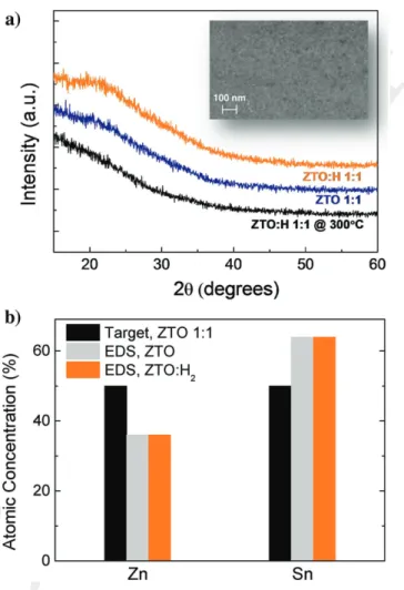
The properties of ZTO thin films annealed at 180 °C were ana-lyzed by X-ray diffraction (XRD) and scanning electron micro-scopy (SEM). The absence of diffraction peaks and the surface smoothness (Figure 1a) support the amorphous nature of the fab-ricated thin films. These properties are not changed by the intro-duction of hydrogen during deposition or by annealing at 300 °C. Despite all ZTO films were produced from a single target with 1:1 composition (Zn:Sn atomic ratio), elemental analysis performed by energy-dispersive X-ray spectroscopy (EDS) reveals that Zn-poorer thin films are obtained relatively to the expected target composition, as seen in Figure 1b. This behavior was already verified for IGZO,[35] being explained by multiphase polycrystalline composition present in the targets and by the different sputtering yields of each one of the
composing phases. The same explanation can be applied to our results, being concomitant with the growth rates obtained in cosputtering using the ceramic targets of the binary com-pounds (for similar deposition conditions, ZnO growth rate is nearly half of SnO2). Furthermore, it should be noticed that no variations in thin films’ composition are detected if hydrogen is added during sputtering and/or after 300 °C annealing.
Spectroscopic ellipsometry was then used to get insights on what could be the role of hydrogen in the fabricated ZTO films. As observed in Figure 2a for ZTO thin films produced with and without hydrogen and annealed at 180 °C the same peak value of the refraction index (n) is obtained, suggesting similar den-sity of both films. The same analysis suggests slightly improved density for films annealed at 300 °C. The amorphous character of ZTO observed before on XRD data is reinforced by analyzing its dependence of the extinction coefficient (k) with energy (Figure 2b): while ZnO:H has a sharp increase of k with E, given that band transitions occur in a well-defined energy range owing to its polycrystalline structure, in amorphous materials as ZTO these transitions occur in a broader range of energy.[36] By using a Tauc–Lorentz model to fit experimental data (see the Experimental Section), further information can be obtained.
Figure 1. Characterization of ZTO thin films annealed at 180 and 300 °C, with and without hydrogen incorporation during sputtering: a) XRD pat-tern, with a SEM surface image of a ZTO film with hydrogen annealed at 180 °C presented as inset; b) elemental analysis obtained by EDS.
UNCORRECTED PROOF
1 2 3 4 5 6 7 8 9 10 11 12 13 14 15 16 17 18 19 20 21 22 23 24 25 26 27 28 29 30 31 32 33 34 35 36 37 38 39 40 41 42 43 44 45 46 47 48 49 50 51 52 53 54 55 56 57 58 59 1 2 3 4 5 6 7 8 9 10 11 12 13 14 15 16 17 18 19 20 21 22 23 24 25 26 27 28 29 30 31 32 33 34 35 36 37 38 39 40 41 42 43 44 45 46 47 48 49 50 51 52 53 54 55 56 57 58 59 www.advancedsciencenews.com www.advelectronicmat.deConsidering 180 °C annealed films, when hydrogen is added the bandgap (Eg) is found to increase from 3.07 to 3.14 eV, being accompanied by a decrease on the parameter C from 4.74 to 2.29. Körner et al.[13,14] theoretically demonstrated by self-interaction correction (SIC) and local density approximation (LDA) models that undercoordinated oxygen-related defects can be moved out of the gap region by the addition of hydrogen. Undercoordinated oxygen atoms were found to be deep levels localized above the valence band (VB) edge (between 0 and 1.5 eV). A hydrogen atom near to these defects is proposed to create an OH bond, making those deep levels disappear into the VB. Such defect annihilation results in a higher bandgap of the semiconductor material. In fact, our analysis seems to have a similar path with those theoretical works: besides the increase of the Eg value, the decrease in C parameter suggests an improvement in material's structural order.[37] A similar trend with H2 incorporation during sputtering is verified for ZTO films annealed at 300 °C but the effect is less significant than for 180 °C annealed films. This could somehow be expected, as
higher annealing temperatures typically overshadow the effect of other processing conditions, as shown before for IGZO films.[38] Interestingly, for films annealed at 300 °C E
g is slightly reduced (3.11 eV) and C parameter slightly increased to 2.41. This should be related with the movement of hydrogen within the film at this temperature and will be further explored during the discussion of Raman data.
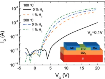
The transfer characteristics of ZTO TFTs on Si/SiO2 sub-strates, whose channel layers were fabricated with and without hydrogen, are shown in Figure 3. Initially, two hydrogen con-centrations during ZTO sputtering were tested, 1 and 2% (safety and mass flow control limitations inhibited the study of further hydrogen contents at this stage). As seen in Figure S1 (Supporting Information), TFTs with higher hydrogen con-tent result in a very significant variation of transfer character-istics after only one week of idle shelf life, particularly in the off-state region. In contrast, devices with 1% H2 in the Ar/O2 atmosphere reveal essentially unchanged properties after one week of idle shelf life. As such, 1% H2 was selected for all the studies presented in this paper. For an annealing temperature of 180 °C the hydrogen incorporation enables a considerable improvement of device performance, particularly of µFE that is increased more than one order of magnitude. Also, the perfor-mance metrics achieved at 180 °C are already quite comparable to the ones obtained for 300 °C annealing, where the enhance-ment effect of hydrogen is considerably less significant. This demonstrates the effectiveness of hydrogen in improving device performance for limited thermal budgets and is perfectly in line with the discussion carried out during spectroscopic ellipsometry analysis on the ZTO thin films.
To be competitive as a transistor technology for circuit appli-cation, ZTO TFTs should be electrically stable under bias and illumination stress. Usually, higher degradation is noted in oxide TFTs when submitted to negative bias illumination stress (NBIS) using wavelengths close to the oxide semiconductor bandgap. This stress condition results in photoionization of oxygen vacancy (V0) related deep defect states to V0+ or V02+ charged states,
0 1 2 3 4 5 6 0.0 0.1 0.2 0.3 0.4 0.5 0.6 0.7 ZnO SnO2 10% O2 10% O2 (@300°C) 10% O2 + 1% H2 10% O2 + 1% H2 (@300°C)
Ex
tintion coefficient,
k
E (eV)
3.00 3.25 3.50 3.75 0.00 0.03 0.06 0 1 2 3 4 5 6 1.8 1.9 2.0 2.1 2.2 2.3 2.4 10% O2 10% O2 (@ 300°C) 10% O2 + 1% H2 10% O2 + 1% H2 (@ 300°C) ZnO SnO2Re
fractive index,
n
E (eV)
a)
b)
Figure 2. Variation of a) refractive index (n) and b) extinction coefficient
(k) as a function of energy (E) for sputtered ZTO thin films, as obtained by spectroscopic ellipsometry. Analysis on binary compounds ZnO and
SnO2 is shown for reference. Inset in (b) shows a magnification at the E
region corresponding to the absorption onset.
Figure 3. Transfer characteristics of ZTO TFTs produced on Si/SiO2 substrates as a function of the hydrogen content during ZTO sputtering and annealing temperature. The inset shows a schematic of the device structure.
UNCORRECTED PROOF
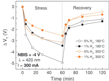
1 2 3 4 5 6 7 8 9 10 11 12 13 14 15 16 17 18 19 20 21 22 23 24 25 26 27 28 29 30 31 32 33 34 35 36 37 38 39 40 41 42 43 44 45 46 47 48 49 50 51 52 53 54 55 56 57 58 59 1 2 3 4 5 6 7 8 9 10 11 12 13 14 15 16 17 18 19 20 21 22 23 24 25 26 27 28 29 30 31 32 33 34 35 36 37 38 39 40 41 42 43 44 45 46 47 48 49 50 51 52 53 54 55 56 57 58 59 donating free electrons to the oxide semiconductor conductionband, decreasing VT.[10,39] For this reason, the instability of ZTO TFTs was tested using VG = -4 V and illumination by blue light (λ = 420 nm) using a high-power LED via an optical fiber for 1 h. The ΔVT evolution during stress and recovery regimes of the four processing conditions under study (with and without H2, for both 180 and 300 °C annealing temperatures) is shown in Figure 4. Regardless of the samples considered the transfer
characteristics exhibit a parallel shift in the negative VG direc-tion with no degradadirec-tion of the subthreshold slope, indicating that creation of defect states at the channel/semiconductor can be neglected. As seen in the same figure the NBIS effect is significantly attenuated when hydrogen is added during ZTO sputtering, owing to the reduction of Vo related defects. This is verified for both 180 and 300 °C annealed films, although it is more significant for the former, corroborating the spectroscopic ellipsometry data. Additionally, for similar processing conditions of ZTO films, the improved material density at higher annealing temperature results in more stable devices.
To further support the experimental results seen on a device level, the ZTO films were analyzed by X-ray photoelectron spec-troscopy (XPS). O 1s peaks analysis is presented in Figure 5, after deconvolution into three subpeaks centered at 530.4 (OI), 531.7 (OII), and 532.7 eV (OIII) using a Gaussian Lorentzian mixed function. These subpeaks can be attributed to O2- ions surrounded by the metallic cations and other oxygen ions (OI), O2- ions in oxygen-deficient regions (OII), and loosely bound oxygen species at the surface, for example, CO3 or adsorbed H2O (OIII).[40,41] Given the high surface sensitivity inherent to XPS technique, a detailed quantitative analysis of the films would require a tight control of the sample transfer between the sput-tering tool and XPS and/or implementation of adequate Ar/Ar cluster ions surface cleaning procedures without inducing chem-ical changes to the specific sample under measurement (which can be challenging on low-temperature deposited oxides,[36] being thus out of the scope of this study. Still, the comparison of the area of OII peak among the different samples suggests that the concentration of oxygen vacancies is significantly decreased
0 20 40 60 80 100 120 -5 -4 -3 -2 -1 0 0% H2, 180°C 1% H2, 180°C 0% H2, 300°C 1% H2, 300°C NBIS = -4 V I = 300 mA Recovery ∆
V
T(V
)
Time (min)
Stress λ = 420 nmFigure 4. Threshold voltage shift as a function of NBIS duration
(including stress and recovery regimes) for ZTO TFTs produced on Si/
SiO2 substrates, as a function of the hydrogen content during ZTO
sput-tering and annealing temperature.
536 534 532 530 528 526
Intens
ity (a
.u
.)
Binding energy (eV)
0 % H2, 180 °C Spectrum OI OII OIII OII=37.06 % 536 534 532 530 528 526 OII=28.33 % In te nsity (a .u .)
Binding energy (eV)
Spectrum OI OII OIII 1 % H2, 180 °C 536 534 532 530 528 526 OII=28.18 % In te ns ity (a.u.)
Binding energy (eV)
Spectrum OI OII OIII 0 % H2, 300 °C 536 534 532 530 528 526 OII=22.70 % In tens ity (a.u .)
Binding energy (eV)
1 % H2, 300 °C
Spectrum OI OII OIII
Figure 5. O 1s XPS spectra obtained for ZTO films with and without hydrogen during sputtering, annealed at 180 and 300 °C. Relative area of the
UNCORRECTED PROOF
1 2 3 4 5 6 7 8 9 10 11 12 13 14 15 16 17 18 19 20 21 22 23 24 25 26 27 28 29 30 31 32 33 34 35 36 37 38 39 40 41 42 43 44 45 46 47 48 49 50 51 52 53 54 55 56 57 58 59 1 2 3 4 5 6 7 8 9 10 11 12 13 14 15 16 17 18 19 20 21 22 23 24 25 26 27 28 29 30 31 32 33 34 35 36 37 38 39 40 41 42 43 44 45 46 47 48 49 50 51 52 53 54 55 56 57 58 59 www.advancedsciencenews.com www.advelectronicmat.dewhen hydrogen is introduced during ZTO deposition. Even if the trend is verified for both 180 and 300 °C annealed films, the largest variation is seen for 180 °C, supporting the NBIS data in Figure 4 and thus the hypothesis that hydrogen can passivate deep traps associated with oxygen vacancies.
2.2. ZTO TFTs with Multicomponent/Multilayer Ta-Si-O Dielectric on Glass and PEN Substrates
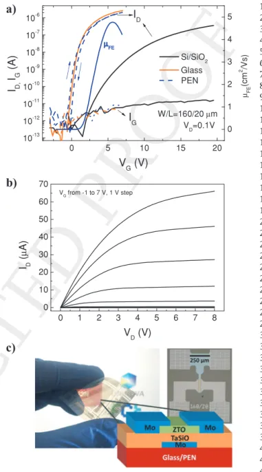
In order to turn the entire transistor stack compatible with flex-ible electronics the thermal SiO2 dielectric layer used for the devices presented so far had to be replaced. Ideal properties for the selected material would be the lowest possible processing temperature (ideally < 200 °C to be compatible with a wide range of polymeric foils) and good interface quality with ZTO, in order to enable stable and low-operating voltage TFTs. Over the last years, sputtered amorphous multicomponent oxide dielectrics have been successfully integrated in IGZO TFTs by our research group,[42–44] fulfilling these requirements. For the present work, a multistack dielectric based on Ta2O5/SiO2 produced by rf magnetron sputtering without intentional sub-strate heating was used to fabricate ZTO TFTs on both glass and PEN foil, using hydrogen during ZTO sputtering and annealing temperature of 180 °C. Figure 6 shows transfer and output characteristics of such devices, being the extracted electrical parameters presented in Table 2. Devices produced on Si/SiO2 are included as reference. Several aspects are clear from this data: first, no relevant differences are found between devices fabricated on glass and PEN, which would be expected considering the low-temperature processing of these transis-tors; second, the operating voltage and subthreshold slope of the ZTO TFTs with the multilayer Ta2O5/SiO2 dielectric are sig-nificantly lower than for devices using thermal SiO2. This is an effect of the high-κ nature of the sputtered multilayer dielec-tric (κ ≈ 14.7), resulting in a higher capacitance per unit area (130 nF cm-2) than with thermal SiO2 (34 nF cm-2); third, µFE is almost duplicated with the multilayer dielectric, reaching similar values to the ones obtained for thermal SiO2 at 300 °C. This µFE enhancement can also be attributed to the increased dielectric capacitance, enabling more effective carrier injection at the semiconductor/dielectric interface. Moreover, it is also noteworthy to mention the good quality of this interface, whose trap density, DIT, can be inferred by
ln10 1 IT I S kT q qD C = + (1)
where k is Boltzmann’s constant (8.62 × 10⁻⁵ eV K-1), and T is
the temperature in degrees. Kelvin, q is the fundamental charge (1.60 × 10
-19 C), and
CI is the capacitance density in F cm-2. DIT values of 1.91 and Q4
Table 1. Electrical properties of ZTO TFTs on Si/SiO2 substrates as a function of hydrogen content and annealing temperature.
Atmosphere TA [°C] Von [V] VT [V] On-off ratio S [V dec-1] µFE [cm2 V-1 s-1]
O2 180 5.1 ± 0.6 18.8 ± 0.6 (1.6 ± 1.1) × 104 1.1 ± 0.3 0.2 ± 0.1 O2/H2 180 1.6 ± 0.2 13.7 ± 0.3 (1.8 ± 1.6) × 106 0.8 ± 0.1 2.6 ± 0.1 O2 300 2.0 ± 0.7 11.5 ± 0.2 (1.1 ± 0.3) × 106 0.7 ± 0.1 4.1 ± 0.1 O2 /H2 300 2.0 ± 1.1 10.4 ± 0.6 (2.8 ± 1.7) × 108 0.5 ± 0.1 5.4 ± 0.2 Q5 0 5 10 15 20 10-13 10-12 10-11 10-10 10-9 10-8 10-7 10-6
I
D Si/SiO2 Glass PENI
D,I
G(A)
V
G(V)
VD=0.1V W/L=160/20 µmI
G 0 1 2 3 4 5 µFE µFE (c m 2 /V s) 0 1 2 3 4 5 6 7 8 0 10 20 30 40 50 60 70 I D ( µ A) VD (V) VG from -1 to 7 V, 1 V stepa)
b)
c)
Figure 6. Electrical properties of ZTO TFTs produced on glass and PEN
substrates, with multilayer Ta-Si-O dielectric. a) Transfer characteristics,
with results on Si/SiO2 being presented as reference. A double sweep
plot is presented for the device on PEN, showing the small magnitude of its clockwise hysteresis; b) output characteristics on PEN substrate. c) A photo, microscopy image, and device schematic of the flexible ZTO TFTs.
UNCORRECTED PROOF
1 2 3 4 5 6 7 8 9 10 11 12 13 14 15 16 17 18 19 20 21 22 23 24 25 26 27 28 29 30 31 32 33 34 35 36 37 38 39 40 41 42 43 44 45 46 47 48 49 50 51 52 53 54 55 56 57 58 59 1 2 3 4 5 6 7 8 9 10 11 12 13 14 15 16 17 18 19 20 21 22 23 24 25 26 27 28 29 30 31 32 33 34 35 36 37 38 39 40 41 42 43 44 45 46 47 48 49 50 51 52 53 54 55 56 57 58 59 7.31 × 1011 cm-2 eV-1 are obtained for thermal SiO2 and the multilayer Ta-Si-O dielectric, respectively. While the latter pre-sents higher DIT, the value is lower than the >1012 cm-2 eV-1 commonly reported for low-temperature processed dielectrics in oxide TFTs.[45,46] Reinforcing the quality of this interface and the advantage of using a high-κ dielectric, the magnitude of clockwise hysteresis, associated with charge trapping at the same interface, is also reduced from 2.15 (thermal SiO2) to 0.43 V (multilayer Ta-Si-O).
The output characteristics show finite resistance on the saturation region, associated with excess carrier concentration at the ZTO layer that cannot be entirely depleted close to the pinch-off region. Still, this deleterious effect is not enough to affect the off-current and/or Von of the devices. Furthermore, no current crowding is observed at low VD range, concomitant with low-contact resistance between Mo source–drain elec-trodes and the ZTO layer.
NBIS measurements on flexible ZTO TFTs under the same stress conditions as used for devices on Si/SiO2 reveal a recov-erable threshold voltage shift of -0.86 V (Figure 7a), which is even lower than the one recorded for the 300 °C annealed ZTO transistors on SiO2 (-2.55 V). While a detailed analysis of the instability mechanisms verified in oxide TFTs with multilayer/ multicomponent dielectrics is beyond the scope of the present paper, it is important to mention that the magnitude and ΔVT direction during stress of oxide TFTs employing these dielectric stacks is dependent on the number of Ta/Si oxide layers and/or Ta-to-Si content. This provides a great route to further improve device stability in the near future.
One of the major concerns of hydrogen doping is its high diffusivity, which could result in a variation of device properties over time and/or under AC operation. During an idle shelf life of five months the static electrical properties of the ZTO TFTs remain essentially unchanged (Figure S2, Supporting Informa-tion). Note that higher hydrogen contents than the ones used in the present work might actually degrade stability, as shown in Figure S1 (Supporting Information). We also analyzed the stability of the flexible ZTO:H TFTs under an AC gate field. For this end, a square-wave between -5 and 5 V with a frequency of 1 kHz was applied to the gate while keeping VD = 5 V, during 15 min. As seen in Figure 7b, Von shifts ≈-1.5 V during stress, with most of this shift occurring during the initial 5 min stress and being recovered after 5 min relaxation. Similar tests were performed with ZTO TFTs on Si/SiO2 substrates, with and without hydrogen (Figure S3, Supporting Information). The data confirm that hydrogen incorporation into ZTO yields devices with improved stability.
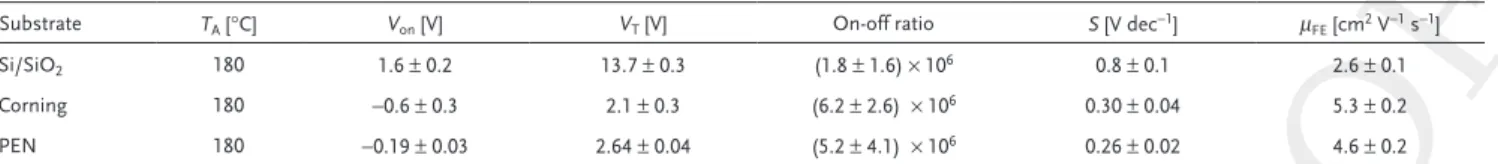
Despite the relatively thick PEN substrates available at this stage (125 µm), preliminary bending tests were performed on the ZTO TFTs, to infer about their applicability as basic
elements of flexible electronic circuits. Figure 8 represents the transfer characteristics of the ZTO TFTs produced on PEN when submitted to different bending radius (r = 15, 25, and 45 mm) using the setup shown in the same figure. The caption inside the transfer plots reflects the order how measurements were made, with “+” and “-” denoting concave and convex bending of the devices, respectively. From Figure 9a, it can be seen a continuous degradation of the gate leakage current (IG) as the bending radius is reduced, resulting in an increased off-current. This degradation is nonrecoverable and presum-ably due to the fracture of the dielectric layer. While a hybrid
Table 2. Electrical properties of ZTO TFTs produced on glass and PEN substrates, with multilayer Ta-Si-O dielectric and annealed at 180 °C. Data for
ZTO TFTs on Si/SiO2 annealed at the same temperature is shown as reference.
Substrate TA [°C] Von [V] VT [V] On-off ratio S [V dec-1] µFE [cm2 V-1 s-1]
Si/SiO2 180 1.6 ± 0.2 13.7 ± 0.3 (1.8 ± 1.6) × 106 0.8 ± 0.1 2.6 ± 0.1 Corning 180 -0.6 ± 0.3 2.1 ± 0.3 (6.2 ± 2.6) × 106 0.30 ± 0.04 5.3 ± 0.2 PEN 180 -0.19 ± 0.03 2.64 ± 0.04 (5.2 ± 4.1) × 106 0.26 ± 0.02 4.6 ± 0.2 0 20 40 60 80 100 120 -1.0 -0.5 0.0 NBIS = -4 V I = 300 mA Recovery ∆
V
T(V
)
Time (min)
Stress λ = 420 nm -5 0 5 10 10-13 10-11 10-9 10-7 10-5I
D(A
)
V
G(V)
Initial 5 min stress 15 min stress 5 min recovery 1% H2, 180 °C VD=0.1 V AC stress (1 kHz):b)
a)
Figure 7. Stability of ZTO TFTs produced on PEN substrates with a
multilayer Ta-Si-O dielectric and annealed at 180 °C: a) threshold voltage
shift as a function of NBIS duration (including stress and recovery regimes); b) transfer characteristics evolution under AC gate stress
UNCORRECTED PROOF
1 2 3 4 5 6 7 8 9 10 11 12 13 14 15 16 17 18 19 20 21 22 23 24 25 26 27 28 29 30 31 32 33 34 35 36 37 38 39 40 41 42 43 44 45 46 47 48 49 50 51 52 53 54 55 56 57 58 59 1 2 3 4 5 6 7 8 9 10 11 12 13 14 15 16 17 18 19 20 21 22 23 24 25 26 27 28 29 30 31 32 33 34 35 36 37 38 39 40 41 42 43 44 45 46 47 48 49 50 51 52 53 54 55 56 57 58 59 www.advancedsciencenews.com www.advelectronicmat.deorganic/inorganic approach to design a new dielectric layer that would have improved mechanical properties while main-taining high-κ could be envisaged, this would necessarily result in a modification of the electrical properties and/or stability. A different approach was thus followed here, by encapsulating the
full device stack with a 1 µm thick Parylene-C layer, deposited by chemical vapor deposition (CVD). Details on the processing and properties of this layer can be found in ref. .[47] As seen in Figure 8b, the performance of the encapsulated ZTO TFTs is insensitive to bending. Preliminary calculations according to the theoretical concepts described in ref.[48] show that the neutral strain point in the transistor stack is inside the rather thick PEN substrate, regardless the existence of this encapsula-tion layer. Nevertheless, the 1 µm thick Parylene film is enough to move critical strain away from the dielectric, improving the bending tolerance of the devices.
2.3. Circuit Integration
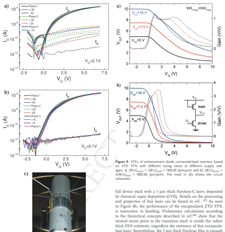
As a demonstration of the applicability of ZTO TFTs for digital and analog flexible oxide electronics, two circuits are presented in this section: an enhancement load inverter and a differential amplifier.
Regarding the inverter, two different devices are shown, based on different sizing strategies for the load and driver TFTs:
-2.5 0.0 2.5 5.0 7.5 10-14 10-12 10-10 10-8 10-6 Plane 1 + 45 - 45 Plane 2 + 25 - 25 Plane 3 + 15 IG
I
D(A
)
V
G(V)
VD=0.1V ID -2.5 0.0 2.5 5.0 7.5 10-14 10-12 10-10 10-8 10-6 Plane 1 +45 -45 Plane 2 +25 -25 Plane 3 +15 -15 Plane 4 IGI
D(A
)
V
G(V)
VD=0.1V IDa)
b)
c)
Figure 8. Bending tests on ZTO TFTs produced on PEN substrates with a
multilayer Ta-Si-O dielectric and annealed at 180 °C: a) transfer characteristics under different bending radius for nonencapsulated devices; b) transfer characteristics under different bending radius for Parylene-encapsulated devices; c) experimental setup to measure devices under bending.
Figure 9. VTCs of enhancement diode connected-load inverters based
on ZTO TFTs with different sizing ratios at different supply
volt-ages: a) (W/L)driver= (W/L)load = 160/20 (µm/µm) and b) (W/L)driver =
3(W/L)load = 480/20 (µm/µm). The inset in (b) shows the circuit
UNCORRECTED PROOF
1 2 3 4 5 6 7 8 9 10 11 12 13 14 15 16 17 18 19 20 21 22 23 24 25 26 27 28 29 30 31 32 33 34 35 36 37 38 39 40 41 42 43 44 45 46 47 48 49 50 51 52 53 54 55 56 57 58 59 1 2 3 4 5 6 7 8 9 10 11 12 13 14 15 16 17 18 19 20 21 22 23 24 25 26 27 28 29 30 31 32 33 34 35 36 37 38 39 40 41 42 43 44 45 46 47 48 49 50 51 52 53 54 55 56 57 58 59 (W/L)driver = (W/L)load = 160/20 (µm/µm) and (W/L)driver =3(W/L)load = 480/20 (µm/µm). The voltage transfer charac-teristics (VTC) of these inverters are depicted in Figure 9, for different VDD. For the former, a gain of 1 V/V is achieved regardless of the VDD, as expected from the sizing strategy. Given the n-type only enhancement load topology, the low level of the output voltage (VOL) deviates significantly from 0 V. To overcome this, the second sizing strategy enables a lower on-resistance of the driver transistor (larger W/L), resulting in VOL ≈ 0 V, with the voltage gain scaling with the sizing ratio of the transistors.
For the analog block, a topology that takes advantage of a positive feedback loop to boost the gain of a regular common-source differential amplifier is used, adapted from ref. [49]. (Figure 10). Considering the small-signal model of Figure 10a,b and Af ≈ 1, the gain can be expressed by
/ / out in m1 o1 o2 V V = −g ×
(
r r)
(2)A microscopy image of the fabricated amplifier is presented in Figure 10c. A high gain of 17 dB can be obtained until ≈1 kHz, being the unity gain frequency ≈ 40 kHz (Figure 10d). The main drawback of this topology is the reduced amplifier bandwidth, although it is still perfectly suitable for a wide range of applications, particularly in smart packaging. Furthermore, the operating frequency can be increased with improved circuit
design (e.g., reduction of channel length and/ or gate-to-source and gate-to-drain overlap to reduce parasitic capacitance), without requiring different deposition/patterning tools for circuit fabrication.
3. Conclusion
In this work, we demonstrate for the first time that sustainable oxide semiconductors as ZTO can be used to obtain flexible TFTs fabricated at only 180 °C with properties com-parable to IGZO TFTs. Hydrogen incorpora-tion during ZTO deposiincorpora-tion demonstrates to be effective in improving the overall elec-trical performance of the devices. Properties such as close-to-0 V Von, on/off ratio ≈106,
S = 0.26 V dec-1, and µ
FE ≈ 5 cm2 V-1 s-1 are obtained for TFTs produced on flexible substrates incorporating a sputtered high-κ multilayer oxide dielectric. This combina-tion of ZTO and Ta-Si-O multilayer dielectric also enables a low ΔVT ≈ -1 V after 1 h NBIS, while a parylene encapsulation layer is found to be critical to turn device performance insensitive to mechanical strain for bending radius down to 15 mm. The potential for digital and analog blocks integration of the ZTO TFTs is demonstrated by an inverter and a differential amplifier with positive feedback loop. While the former enables rail-to-rail operation with VDD as low as 5 V, the latter exhibits a gain of 17 dB and unity gain frequency of 40 kHz, which can be fur-ther improved in future designs by reducing channel length and parasitic capacitance.
ZTO TFTs can thus be seen as the basis of a next generation of high-performance and flexible electronic systems where sus-tainability plays a crucial role.
4. Experimental Section
ZTO Deposition and TFT Fabrication: Staggered bottom-gate, top-contact TFTs were produced using two different structures. In structure A (inset in Figure 3), p-type Si was used as substrate/gate
electrode and 100 nm thick thermally grown SiO2 as dielectric. The
ZTO semiconductor layer (40 nm) was deposited without intentional substrate heating by rf magnetron sputtering, using a 2 in. ceramic ZTO
target (Zn:Sn atomic ratio of 1:1) and Ar+O2 or Ar+O2+H2 atmospheres.
Then, Mo (60 nm) source–drain electrodes were sputtered on top of ZTO. Both semiconductor and electrodes were patterned by optical photolithography to achieve devices with width-to-length ratios (W/L) of 160/20 (µm/µm). In structure B (Figure 6b), 0.7 mm thick Corning
Eagle glass or 125 µm thick PEN was employed as substrate and
sputtered Mo (60 nm) as gate electrode. Replacing the thermally grown
SiO2 of structure A, a 100 nm thick multilayer/multicomponent dielectric
was cosputtered without intentional substrate heating using SiO2 and
Ta2O5 2 in. targets, followed by dry etching process in SF6 atmosphere
to access the gate electrode. Then, ZTO and Mo source–drain electrodes were processed as in structure A, also resulting in TFTs with
W/L = 160/20 (µm/µm) (Figure 6c). The devices were finally annealed
Figure 10. Differential amplifier based on ZTO TFTs: a) circuit schematic, adapted from ref.[49] showing the common source amplifier with a positive feedback unit; b) circuit schematic with the feedback network expanded; c) microscopy image of the fabricated amplifier; d) frequency response of the amplifier.
UNCORRECTED PROOF
1 2 3 4 5 6 7 8 9 10 11 12 13 14 15 16 17 18 19 20 21 22 23 24 25 26 27 28 29 30 31 32 33 34 35 36 37 38 39 40 41 42 43 44 45 46 47 48 49 50 51 52 53 54 55 56 57 58 59 1 2 3 4 5 6 7 8 9 10 11 12 13 14 15 16 17 18 19 20 21 22 23 24 25 26 27 28 29 30 31 32 33 34 35 36 37 38 39 40 41 42 43 44 45 46 47 48 49 50 51 52 53 54 55 56 57 58 59 www.advancedsciencenews.com www.advelectronicmat.deat 180 or 300 °C for 1 h in air (hot plate). Selected devices for bending
tests were also passivated with a 1 µm thick parylene layer, which was
patterned using a dry etching process in O2 atmosphere to access the
gate, source, and drain electrodes.
Thin Film, TFT, and Circuit Characterization: To study the structural properties of the ZTO thin films, XRD measurements were performed at room temperature using a PANalytical X’Pert Pro X-ray diffractometeter in Bragg–Brentano geometry with a monochromatic Cu Kα line radiation (λ = 1.540598 Å). Elemental analysis was carried out by EDS using an Oxford X-Max 150 detector inside a Zeiss Auriga Crossbeam workstation, which was also used to evaluate surface topography. The optical properties were obtained by spectroscopic ellipsometry, using a Jobin Yvon Uvisel ellipsometer. The Tauc–Lorentz model was used to
described the dielectric function (ε) that is the sum of the real (ε1) and
imaginary (ε2) parts, in which[37]
1 0 2 TL g 2 2 TL2 2 2 2 g g E AE C E E E E C E E E E E ε =
(
(
)
)
− − + → > → < (3)where A is related to the strength of the absorption peak; ETL is the
energy of maximum transition; Eg the optical bandgap and C the
broadening term that is inversely proportional to material’s structural order in a short distance. All the fitted parameters are given in eV.
XPS measurements were carried out with a Kratos Axis Supra, using monochromated Al Kα irradiation (1486.6 eV). The detail spectra were acquired under an emission angle of 90° with a pass energy of 5 eV, resulting in an energy resolution better than 0.45 eV. Due to the accumulation of charges during the measurement, the peak positions were shifted by moving the C 1s main component to 284.8 eV.
Static electrical characterization of TFTs and inverters was performed using an Agilent 4155C semiconductor parameter analyzer and a Cascade Microtech M150 probe station. Stability under NBIS was evaluated using a Keithley 4200SCS semiconductor parameter analyzer and a Janis ST-500 probe station, with a high-power LED with emission centered at 420 nm and directed to the sample surface using a micropositioner with an optical fiber. AC stress measurements were performed using a Wavetek 395 waveform generator to apply a square wave signal to the gate electrode with frequency of 1 kHz, peak-to-peak
voltage of 10 V, and offset of 5 V, while keeping VD= 5 V. Regarding the
differential amplifier, its characterization was performed using a custom-designed printed circuit board (PCB) with a buffer to suppress load
capacitances from the measurement system. 2 V biasing (VB1= VB2),
VDD= 8 V, and two complementary sine waves were used as inputs, with
amplitude and offset of 200 mV and 2.5 V, respectively. An ISO-TECH IDS 8062 oscilloscope was used to monitor the output signal. All the measurements were performed in air at room temperature.
Supporting Information
Supporting Information is available from the Wiley Online Library or from the author.
Acknowledgements
This work was funded by FEDER funds through the COMPETE 2020 Program and National Funds through FCT – Portuguese Foundation for Science and Technology under Project No. POCI-01-0145-FEDER-007688, Reference No. UID/CTM/50025. This work also received funding from the H2020 European Research Council under Grant Agreement Nos. 716510 (ERC-2016-STG TREND), 644631 (Roll-Out), 692373 (BET-EU), and 685758 (1D-Neon). The authors gratefully acknowledge Prof. Luís Pereira for the discussion on spectroscopic ellipsometry results.
Conflict of Interest
The authors declare no conflict of interest.
Keywords
amorphous semiconductors, flexible electronics, oxide TFT, sustainable materials, zinc-tin oxide
Received: January 16, 2018 Revised: March 23, 2018 Published online:
[1] H. Kumomi, S. Yaginuma, H. Omura, A. Goyal, A. Sato, M. Watanabe, M. Shimada, N. Kaji, K. Takahashi, M. Ofuji, T. Watanabe, N. Itagaki, J. Disp. Technol. 2009, 5, 531.
[2] E. Fortunato, P. Barquinha, R. Martins, Adv. Mater. 2012, 24, 2945. [3] J. S. Park, W.-J. Maeng, H.-S. Kim, J.-S. Park, Thin Solid Films 2012,
520, 1679.
[4] K. Nomura, H. Ohta, A. Takagi, T. Kamiya, M. Hirano, H. Hosono, Nature 2004, 432, 488.
[5] http://ec.europa.eu/growth/sectors/raw-materials/specific-interest/ critical/index_en.htm.
[6] H. Q. Chiang, J. F. Wager, R. L. Hoffman, J. Jeong, D. A. Keszler, Appl. Phys. Lett. 2005, 86, 13503.
[7] R. L. Hoffman, Solid State Electron. 2006, 50, 784.
[8] M. G. McDowell, R. J. Sanderson, I. G. Hill, Appl. Phys. Lett. 2008, 92, 10.
[9] W.-S. Cheong, S.-M. Yoon, J.-H. Shin, C.-S. Hwang, J. Korean Phys. Soc. 2009, 54, 544.
[10] H. W. Lee, B. S. Yang, Y. J. Kim, A. Y. Hwang, S. Oh, J. H. Lee, J. K. Jeong, H. J. Kim, IEEE Trans. Electron Devices 2014, 61, 3191. [11] K. Okamura, D. Nikolova, N. Mechau, H. Hahn, Appl. Phys. Lett.
2009, 94, 183503.
[12] D. Han, Y. Zhang, Y. Cong, W. Yu, X. Zhang, Y. Wang, Sci. Rep. 2016, 6, 38984.
[13] W. Körner, P. Gumbsch, C. Elsässer, Phys. Rev. B 2012, 86, 165210. [14] W. Körner, C. Elsässer, Thin Solid Films 2014, 555, 81.
[15] T. Kim, Y. Nam, J.-H. Hur, S.-H. K. Park, S. Jeon, Nanotechnology
2016, 27, 325203.
[16] M. Miyakawa, M. Nakata, H. Tsuji, Y. Fujisaki, T. Yamamoto, AIP Adv. 2016, 6, 85016.
[17] R. Takenouchi, T. Toda, R. Ishii, H. Takahashi, D. Wang, M. Furuta, IMID 2015 Dig. 2015, 86, 13503.
[18] J. Bang, K. J. Chang, Appl. Phys. Lett. 2008, 92, 10.
[19] H. R. Kim, D. H. Kim, E. Byon, G. H. Lee, G. H. Lee, P. K. Song, Jpn. J. Appl. Phys. 2010, 49.
[20] D. Hong, H. Q. Chiang, R. E. Presley, N. L. Dehuff, J. P. Bender, C.-H. Park, J. F. Wager, D. A. Keszler, Thin Solid Films 2006, 515, 2717.
[21] P. Görrn, M. Sander, J. Meyer, M. Kröger, E. Becker, H.-H. Johannes, W. Kowalsky, T. Riedl, Adv. Mater. 2006, 18, 738.
[22] P. Görrn, P. Hölzer, T. Riedl, W. Kowalsky, J. Wang, T. Weimann, P. Hinze, S. Kipp, Appl. Phys. Lett. 2007, 90, 23.
[23] P. Görrn, M. Lehnhardt, T. Riedl, W. Kowalsky, Appl. Phys. Lett.
2007, 91, 193504.
[24] T. Riedl, P. Görrn, P. Hölzer, W. Kowalsky, Phys. Status Solidi RRL
2007, 1, 175.
[25] T. Riedl, P. Gorrn, W. Kowalsky, IEEE/OSA J. Disp. Technol. 2009, 5, 501.
[26] P. Görrn, T. Riedl, W. Kowalsky, J. Phys. Chem. C 2009, 113, 11126. [27] P. Görrn, F. Ghaffari, T. Riedl, W. Kowalsky, Solid State Electron.
2009, 53, 329.
UNCORRECTED PROOF
1 2 3 4 5 6 7 8 9 10 11 12 13 14 15 16 17 18 19 20 21 22 23 24 25 26 27 28 29 30 31 32 33 34 35 36 37 38 39 40 41 42 43 44 45 46 47 48 49 50 51 52 53 54 55 56 57 58 59 1 2 3 4 5 6 7 8 9 10 11 12 13 14 15 16 17 18 19 20 21 22 23 24 25 26 27 28 29 30 31 32 33 34 35 36 37 38 39 40 41 42 43 44 45 46 47 48 49 50 51 52 53 54 55 56 57 58 59[28] M. Fakhri, P. Görrn, T. Weimann, P. Hinze, T. Riedl, Appl. Phys. Lett.
2011, 99, 123503.
[29] M. Fakhri, H. Johann, P. Görrn, T. Riedl, ACS Appl. Mater. Interfaces
2012, 4, 4453.
[30] M. Fakhri, N. Babin, A. Behrendt, T. Jakob, P. Görrn, T. Riedl, Adv. Mater. 2013, 25, 2821.
[31] W. B. Jackson, R. L. Hoffman, G. S. Herman, Appl. Phys. Lett. 2005, 87, 1.
[32] W. B. Jackson, G. S. Herman, R. L. Hoffman, C. Taussig, S. Braymen, F. Jeffery, J. Hauschildt, J. Non-Cryst. Solids 2006, 352, 1753. [33] C.-K. Lee, H. Y. Jung, S. Y. Park, B. G. Son, C.-K. Lee, H. J. Kim,
R. Choi, D.-H. Kim, J.-U. Bae, W.-S. Shin, J. K. Jeong, IEEE Electron Device Lett. 2013, 34, 253.
[34] C. K. Lee, A. Y. Hwang, H. Yang, D. H. Kim, J. U. Bae, W. S. Shin, J. K. Jeong, IEEE Trans. Electron Devices 2013, 60, 4165.
[35] A. Olziersky, P. Barquinha, A. Vila, C. Magana, E. Fortunato, J. R. Morante, R. Martins, Mater. Chem. Phys. 2011, 131, 512. [36] P. Barquinha, Ph.D. Thesis, Faculdade de Ciências e Tecnologia,
Universidade NOVA de Lisboa, Almada 2010.
[37] L. Pereira, Ph.D. Thesis, Faculdade de Ciências e Tecnologia, Univer-sidade NOVA de Lisboa, Almada 2008.
[38] P. Barquinha, L. Pereira, G. Gonçalves, R. Martins, E. Fortunato, Electrochem. Solid-State Lett. 2008, 11, H248.
[39] B. S. Yang, S. Oh, Y. J. Kim, S. J. Han, H. W. Lee, H. J. Kim, S. Kim, H. K. Park, J. Heo, J. K. Jeong, H. J. Kim, IEEE Trans. Electron Devices
2014, 61, 2071.
[40] J. Kim, S. Bang, S. Lee, S. Shin, J. Park, H. Seo, H. Jeon, J. Mater. Res. 2012, 27, 2318.
[41] M. Miyakawa, M. Nakata, H. Tsuji, Y. Fujisaki, T. Yamamoto, AIP Adv. 2016, 6, 085016.
[42] P. Barquinha, L. Pereira, G. Gonçalves, R. Martins, D. Kušcˇer, M. Kosec, E. Fortunato, J. Electrochem. Soc. 2009, 156, H824. [43] P. G. Bahubalindruni, V. G. Tavares, R. Martins, E. Fortunato,
P. Barquinha, IEEE Trans. Circuits Syst. IRegular Pap. 2017, 64, 1118. [44] L. Pereira, P. Barquinha, E. Fortunato, R. Martins, D. Kang,
C. J. Kim, H. Lim, I. Song, Y. Park, Thin Solid Films 2008, 516, 1544. [45] Y. R. Liu, H. Huang, P. T. Lai, W. J. Wu, R. S. Chen, J. Phys. Commun.
2017, 1, 35003.
[46] Y. Lin, J. Chou, J. Nanomater. 2015, 2015, 1.
[47] A. Kiazadeh, H. L. Gomes, P. Barquinha, J. Martins, A. Rovisco, J. V. Pinto, E. Fortunato, J. V. Pinto, R. Martins, E. Fortunato, Appl. Phys. Lett. 2016, 109, 051606.
[48] S. Wagner, H. Gleskova, I.-C. Cheng, J. C. Sturm, Z. Suo, Flexible Flat Panel Displays, Wiley, Chichester, UK 2005, p. 263.
[49] Y. Tarn, P. Ku, H. Hsieh, L. Lu, IEEE J. Solid-State Circuits 2010, 45, 1028.