Single VDTA Based Multifunction
Trans-admittance mode Biquad Filter
Chandra Shankar #1 , Sajai Vir Singh*2 #Dept. of Electronics Engineering , #
JSS Academy of Technical Education Noida, 201301, INDIA Dept. of Electronics and Communication Engineering
*Jaypee Institute of Information Technology, Noida, 201304, INDIA 1
2
Abstract— This paper proposed a multifunction biquad filter topology using only single VDTA as active element. In addition, it uses one grounded resistor, two capacitors and capable of realizing trans-admittance mode low pass (LP), high pass (HP), band pass (BP), and band reject (BR) biquad filtering response, simultaneously, by the use of single voltage input signal only. Apart from this, the proposed circuit has many excellent features such as, low active and passive sensitivity, low power consumption, canonical structure and electronic tunability of pole frequency and quality factor. To justify the theoretical analysis, the proposed circuit is simulated using PSPICE in 0.18μm CMOS technology from TSMC.
Keyword- Biquad, TAM ,VDTA, Filter, Analog signal processing, Electronic tunable, multifunction. I. INTRODUCTION
In now a days current-mode active elements are being preferably used in the designing of analog filter and other analog circuits also due to offering many advantages such as wider signal bandwidth, low power consumption, larger dynamic range, better linearity, simple circuitry and requirement of lesser on chip area [1]-[27] over voltage-mode counterpart (such as op-amp). One type of analog filter named as trans-admittance mode filer which uses voltage signal as input and provide current signal in the form of output and hence, it can act as interface filter circuits connecting voltage-mode to current-mode in number of applications such as receiver base band blocks of modern radio system where conversion of voltage signal to current signal is required [16]-[18],[25].
In available literature, the numbers of papers proposing biquad filtering topology operating in trans-admittance-mode have been found which are further classified either as multi input single output (MISO) [23]-[25] or single input multi output (SIMO) [15]-[22],[27] on the basis of number of input and output signals involved in the circuits. However, it is also noted that MISO structure offers the disadvantage over SIMO structure in the sense it requires multiple copies of the input signals which further requires additional hardware to implement multiple copies of input signals and realizes only one filtering function at a time. On the other hand, SIMO require only one input signal and realizes more than one filtering functions simultaneously. Table.1 is showing the detailed comparative study of SIMO TAM biquad filter [15]-[22],[27] which can conclude that most of the circuits realizes only three filtering functions simultaneously and except [27], uses more than one active element in the filtering functions realization. Few of them employ more number of passive elements [15]-[16] and does not provide the feature of electronic tunability of pole frequency (ω0), quality factor (Q0) too
[15]-[16],[18],[21].
After looking the facts from above discussion, we have proposed a new single input four output trans-admittance-mode biquad filter by the use of only single VDTA, and three passive elements (one resistor and two capacitors) and can realize LP, HP, BP, BR filtering functions, simultaneously. Moreover, ω0 can also be tuned
electronically independent of Q0. The circuit possesses low active and passive sensitivity. The proposed circuit
has been simulated on PSPICE simulation tools (ORCAD 16.3) to justify its performance.
II. VDTADESCRIPTION
±
−
=
±
Z N P
m m
m
X z
V
V
V
g
g
g
I
I
2 1
1
0
0
0
(1)
Here, gm1 and gm2 are transconductance parameters of first and second stage of VDTA, respectively whose value are controlled by biasing current IB1 and IB2 of VDTA, respectively. A CMOS transistors implementation of VDTA is also shown in Fig.2. For this realization, mathematical expression of gm1 and gm2 can be derived [25] as.
2 , 1 1
1 B n ox
(
)
M Mm
L
W
C
I
g
=
µ
(2)
2 2 5, 6
)
(
M Mox n B m
L
W
C
I
g
=
µ
(3) Where µnis the effective carrier mobility of MOS transistor and Cox is the gate-oxide capacitance per unitarea. (W/L)M1, M2 and (W/L) M5, M6 are the aspect ratio of M1, M2 and M5, M6 NMOS transistor pairs,
respectively.
Fig. 1. Block diagram of VDTA
III. PROPOSED TAMFILTER AND ITS ANALYSIS
Fig.3 shows the proposed TAM filter configuration which employs one VDTA, two capacitances (C1 and C2)
with one of the capacitor (C1) being grounded and one grounded resistor (R). The following transfer functions
described in (4)–(7) can be obtained after analysing the proposed circuit in Fig.3.
(
)
2 1 2 1s
D
R
C
C
g
g
V
I
m m in LP=
−
(4)
(
)
1 1s
D
R
C
sg
V
I
m in BP=
(5)(
)
2s
D
R
s
V
I
in HP=
(6)(
)
1
2 1 2 1 2s
D
R
C
C
V
g
g
s
V
I
in m m in BR
+
=
(7)Fig. 3. Proposed TAM Biquad filter References
Features [15] [16] [17] [18] [19] [20] [21] [22] [27] Proposed Nos & types of
Active element’s.
3-PFTFN
3- CCII 2-CCCCTA
3- CCCII
4- OTA 4-OTA 5-DCC-DVCC
2-VDTA
1-VDTA 1-VDTA
Nos. & types of Passive element’s
3-R ,
2-C 3-R ,2-C 3-C 2-C 2-C 2-C 2-C, 1-R 2-C 1-R, 2-C 1-R, 2-C
No. of Floating passive element
4(2-R+ 2-C)
4 (2-R+
2-C) NIL NIL NIL NIL 3(2-R+
1-C) NIL 1(1-R) 1(1-C)
Functions Realized LP, HP, BP LP, HP BP LP, HP BP LP, HP BP, BR LP, HP BP LP, HP BP LP, HP BP LP, HP
BP HP ,BP
LP, HP BP, BR
Electronic
where
+
+
=
2 1 2 1 1 2)
(
C
C
g
g
R
C
s
s
s
D
m m(8) It can be noted that from (4)-(7), the proposed topology as shown in Fig.3 is capable of realizing trans-admittance-mode LP, BP, HP and BR filtering responses. The characterized parameters of the proposed filter like pole frequency (ω0), quality factor (Q0) and bandwidth (BW) can be derived as
1 2 2 1 0
C
C
g
g
m m=
ω
(9) 2 2 1 1 0C
g
g
C
R
Q
m m=
(10)C
R
BW
11
=
(11) It is clear from (9)-(10) that ω0 can be tuned electronically independent of Q0 by maintaining the conditionsgm1 = gm2 = 1/R.
IV. NON IDEAL ERRORS AND SENSITIVITY ANALYSIS
In this section, the effect of non-ideal errors of VDTA occurring due to mismatching in MOS transistors in CMOS implementation on the the performance of the proposed circuit is considered. By taking non-ideal errors of VDTA into consideration, the current and voltage relation between various ports of VDTA can be rewritten as:
±
−
=
± Z N P m m m X zV
V
V
g
g
g
I
I
2 2 1 1 1 10
0
0
β
β
β
(12)Where β1 and β2 are named as the tracking error for the first and second stages of VDTA. Now, by considering non-ideal errors discussed in (12), the proposed circuit of Fig.3 is further reanalyse to obtain various TAM transfer functions and characteristic parameters. The resultant expressions are derived as
(
)
2 1 2 1 2 1s
D
R
C
C
g
g
V
I
m m in LPβ
β
−
=
(13)(
)
1 1 1s
D
R
C
g
s
V
I
m in BPβ
=
(14)(
)
2s
D
R
s
V
I
in HP=
(15) ( ) 1 2 1 2 1 2 1 2 s D R C C V g g S V I in m m in BR + =β
β
(16)Where
+
+
=
2 1 2 1 2 1 1 2)
(
C
C
g
g
R
C
s
s
s
D
β
β
m m(17)
1 2 2 1 2 1 0
C
C
g
g
m mβ
β
ω
=
(18) 2 2 1 1 2 1 0C
g
g
C
R
Q
=
β
β
m m(19) C R BW 1 1 = (20)
It can be noted that that filter parameters such as pass band gain, ω0, and Q0 may deviate slightly due to effect of tracking errors of VDTAs. But the effect of these changes can be minimized by selecting proper electronic controllable trans-conductance parameters.
The active and passive sensitivities of ω0and Q0 for proposed filter in Fig.3 are also calculated and described in following set of equations.
2
1
,
2
1
0 2 , 1 0 2 ,1
=
=
ω ω
β
β
S
gm gmS
(21)
2
1
02 ,
1
=
−
ω C C
S
(22)
2
1
,
2
1
0 2 , 1 0 2 ,1
=
=
Q g g Q m m
S
S
β β (23)
2
1
,
2
1
0 2 01
=
=
−
Q C Q
C
S
S
(24)
1
0
=
Q R
S
(25) Above results explained that all sensitivities of ω0and Q0 are low and less than unity in magnitude.V. SIMULATION RESULT
In order to justify the theoretical discussion in previous sections, various PSPICE simulations of the proposed circuit were performed using CMOS realization of VDTA in 0.18µm CMOS technology from TSMC [24]. The power supply voltage and biasing currents were taken as VDD = -VSS = 1.1V and IB1 = IB2 = 58µA (gm1
= gm2 ≈ 495.0µA/V). The passive component values were also selected as R= 2.05KΩ, C1 = C2 = 20pF. The
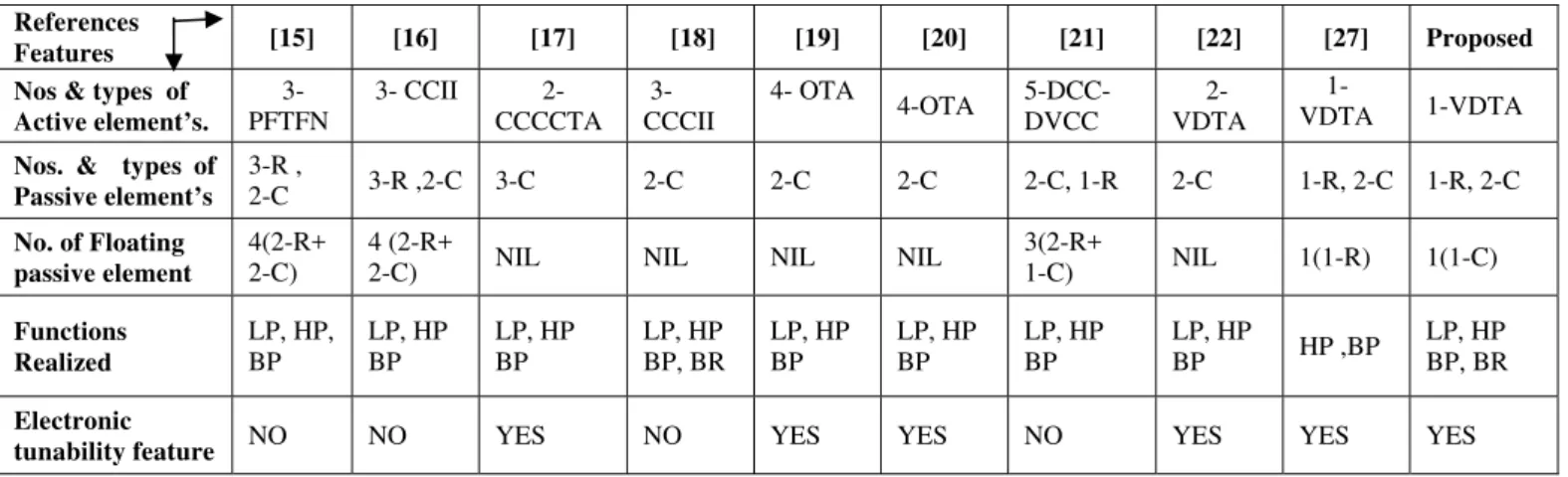
aspect ratios of various transistors were determined as given in Table II. Fig.4 shows the ideal and PSPICE simulated TAM gain responses of LP, HP, BP, and BR filtering functions of the proposed biquad filter. It is clear from Fig.4 that ideal and PSPICE simulated results are almost same and the simulated value of the pole frequency was obtained as 3.94 MHz which is nearly same as the calculated value of 3.95 MHz.
An electronically tuning behaviour of the proposed circuit in term of pole frequency (f0) variation
independent of Q0 was also shown in Fig.5 which was obtained by simulating various TAM BP filtering
functions at constant Q0. To see the transient behaviour of the circuit, it was further simulated for LP output by
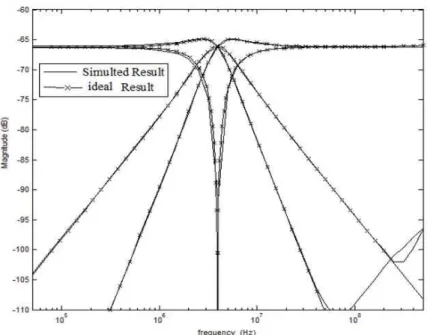
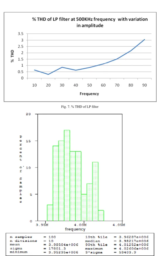
applying a sinusoidal input voltage signal having peak to peak amplitude of 50mV at frequency of 500 KHz. Fig.6 shows the simulated result of the transient response of LP output which was obtained across 2 KΩ load resistor connected across the LP filtering response. In addition, Fig.7 shows the total harmonic distortion (THD) results for LP responses which can clearly conclude that the THD values of the proposed filter for LP voltage output across resistor was found in the range of .644 to 3.06% for sinusoidal input voltage signal of constant frequency of 500 KHz and variable peak to peak amplitude of 20mV to 180mV. Furthermore, Monte-Carlo analysis was also carried out to observe the tolerance variation of passive components. The TAM BP output with 10% Gaussian deviation in C1 = C2 = 20pF has been simulated. The simulation was performed concurrently
Fig. 4. Ideal and PSPICE simulated response of LP,HP,BP,BR TAM Filter
Fig. 7. % THD of LP filter
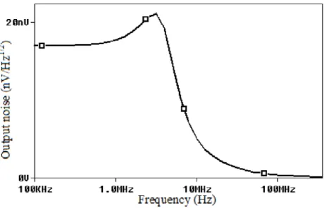
Fig. 9. Output noise density of band pass filter
TABLEII. TRANSISTORS ASPECT RATIOS OF THE CIRCUIT SHOWN IN FIG.2
Transistor W(µm)/L(µm)
M1,M2,M5,M6 M3,M4 M7-M13 M14-M18
8.28/.36 14.4/.36 4.32/.36 3.6/.36
VI. CONCLUSION
In this paper, a new biquad filter circuit is realized using single VDTA, one grounded resistors and two capacitors with one of the capacitor being grounded which is competent of simultaneously realizing trans-admittance-mode LP, BP, HP, and BR filtering responses by the use of single voltage input signal. Apart from these features, the proposed circuit offers the following other features also.
i. Use of minimum number of active element (only single) to realize four filtering responses simultaneously in TAM.
ii. Use of one grounded resistor only. iii. Low active and passive sensitivities. iv. Low power dissipation.
v. Filter parameters such as ω0 and Q0 are electronically tuned.
vi. Providing canonical structure as having only two capacitors.
REFERENCES
[1] D. Biolek, R. Senani, V. Biolkova and Z. Kolka, “Active elements for analog signal processing: classification, review, and new proposals,” Radioengineering J., Vol. 17, pp. 15-32, December 2008.
[2] C. Toumazou, F. J. Lidgey and D. G. Haig, Analogue IC design: the current-mode approach, London, UK, Peteregrinus Ltd., 1990. [3] S. V. Singh , S. Maheshwari and D. S. Chauhan, “Single MO-CCCCTA- based electronically tunable current/Trans-impedance-mode
biquad universal filter,” Circuit and system vol.2, pp.1-6, 2011.
[4] M.Siripruchyanun, W.Jaikla, “CMOS current-controlled current differencing transconductance amplifier and applications to analog signal processing,” AEU-Int. J. Electron. Commun., Vol. 62, pp. 277-287, 2008.
[5] S. Maheshwari, S. V. Singh and D. S. Chauhan, “Electronically tunable low voltage mixed-mode universal biquad filter,” IET Circuits, Devices and Systems, Vol 5, pp. 149-158,2011.
[6] Ü. Keskin, D. Biolek, E. Hancioglu and V. Biolkova,” Current-mode KHN filter employing current differencing transconductance amplifiers,” Int’l J. Electronics and Communications (AEÜ), Vol. 60, pp. 443-446, 2006.
[7] S. V. Singh, S. Maheshwari, and D. S. Chauhan, “Electronically tunable CCCCTA-based cascadable current-mode universal biquad filter,” J. Active and Passive Electronic Devices, USA, Vol. 9, No. 1, pp. 39-51, 2014.
[8] S. Maheshwari, “High performance voltage-mode multifunction filter with minimum component count,” WSEAS Transations on Electronics, Vol. 5, pp. 244-249, 2008.
[9] S. Minaei, O. K. Sayin and H. Kuntman, “A new CMOS electronically tunable current conveyor and its application to current-mode filters,” IEEE Tran. Circuits and Systems-I, Vol. 53, No. 7, pp. 1448-1457, 2006.
[10] R. S. Tomar, S. V. Singh and D. S. Chauhan, “Cascadable low voltage operated current-mode universal biquad filter,” WSEAS Transactions on Signal Processing, Vol. 10, pp. 345-353, 2014.
processing ,Vol. 27, pp. 405- 427, 2008.
[14] S. Minaei, G. Topcu and O. Cicekoglu, “Low input impedance trans-impedance type multifunction filter using only active elements,” International J. Electronics, Vol. 92, No. 7,pp. 385-392, 2005.
[15] N. A. Shah, S. Z. Iqbal and B. Parveen, “SITO high output impedance trans-admittance filter using FTFNs,” Analog Integrated Circuits and Signal Processing, Vol. 40, No. 4, pp. 87-89, 2004.
[16] A. Toker, O. ÇiÇekoglu, S. Özcan and H. Kuntman, “High output impedance trans-admittance type continuous time multifunction filter with minimum active elements,” Int’l J. Electronics, Vol. 88, No. 10, pp. 1085-1091, 2001.
[17] S. V. Singh, S. Maheshwari, J. Mohan and D. S. Chauhan, “An electronically tunable SIMO biquad filter using CCCCTA,” Contemporary Computing, CCIS, Vol. 40, pp. 544-554, 2009.
[18] N. Pandey, S. K. Paul, “SIMO trans-admittance-mode active-C universal filter,” J. Circuits and Systems, Vol. 1, pp. 54-58, 2010. [19] D. R. Bhaskar, A. K. Singh, A. K. Sharma and R. Senani, “New OTA-C universal current-mode/trans-admittance biquads,” IEICE
Electronics Express, Vol. 2, pp. 8-13, 2005.
[20] M. A. Ibrahim and H. Kuntman,” A novel trans-admittance-type biquad employing DO-OTA with only two grounded capacitors,” Proc. IEEE 13th Int’l Conf. Signal Processing and Communications Applications, pp. 119-122, 2005.
[21] P. Beg, S. Maheshwari and M. Siddiqi, “Digitally controlled fully differential voltage-and trans-admittance-mode biquadratic filter,” IET Circuits, Devices and Systems, Vol. 7, pp. 193-203, 2013.
[22] D. Prasad, M. Srivastava and D. R. Bhaskar, “Trans-admittance type universal current-mode biquad filter using VDTAs,” International Scholary Research Notice, Vol. 2014, Article ID-762845, pp. 1-4, 2014.
[23] N. A. Shah, M. Quadri and S. Z. Iqbal, “CDTA based universal trans-admittance filter,“ Analog Integrated Circuits and Signal Processing, Vol. 52, pp. 65-69, 2007.
[24] G.Gupta, S.V.Singh, S.V. Bhooshan, ”VDTA Based Electronically Tunable Voltage-Mode and Trans-Admittance Biquad Filter” Circuits and Systems, 6, pp.93-102,2015.
[25] C.Shankar, S.V.Singh “ A New Trans-admittance Mode Biquad Filter using MO-VDTA”, WSEAS transaction on Circuits and Systems, pp.8-18,vol.14, 2015.
[26] A. Yesil, F. Kacar and H. Kuntman, “New simple CMOS realization of voltage differencing trans-conductance amplifier and its RF filter application,” Radioengineering, Vol.20 , No.3, pp. 632-637, 2011.
[27] C.Shankar, S.V.Singh,”A low voltage operable VDTA based biquad filter realizing band pass and high pass filtering functions in trans-admittance-mode,” ICCCA-2015,pp.1288-1293,MAY,2015.
AUTHORPROFILE
Chandra Shankar was born in Etawah, India. He received his B.Tech degree in Electronics and Communication from GLAITM, Mathura (India), M.Tech. degree from CDAC, Mohali (India) and Pursuing Ph.D from Jaypee Institute of Information Technology, Noida (India). He is working as an Asst. Professor in the Dept. of Electronics of JSS Academy of Technical Education Noida, (India). His area of interest is Analog Signal Processing and Circuit Designing.