An upgraded TOF-SIMS VG Ionex IX23LS: study on the negative secondary ion emission of III-V compound semiconductors with prior neutral cesium deposition
C. A. A. Ghumman, A. M. C. Moutinho, A. Santos, O. M. N. D. Teodoro, and A. Tolstogouzov∗
Centre for Physics and Technological Research (CeFITec), Dept. de Física da Faculdade de Ciên-cias e Tecnologia (FCT), Universidade Nova de Lisboa, 2829-516 Caparica, Portugal
Abstract
An upgraded TOF-SIMS VG Ionex IX23LS was used to study the secondary emission of negative atomic and cluster ions of non-metallic elements (P, As and Sb) upon 19 keV Ga+ bombardment of non-degenerated III-V semiconductors (GaP, GaAs, GaSb, InP, InAs and InSb) with prior neutral Cs deposition from getter dispenser.
The instrument data acquisition and control system was upgraded resulting in reliable and easy to use equipment. This instrument became suitable to be used in routine and research analysis for a many more years, as we show in the present application.
It was found that surface cesiation results in the peak intensity enhancement of any negative sec-ondary ion species; in case of atomic ions the greatest increase (360) was obtained for P- emitted from InP. Such enhancement was higher for In-based compounds than for Ga-based ones. We ex-plained that in terms of the electronegativity difference between atoms composing III-V semicon-ductors. The greater electronegativity difference (bond ionicity) of In-based compounds resulted in the greater Cs-induced work function decrease leading to a higher increase in the ionization proba-bility of secondary ions.
Keywords: TOF-SIMS; III-V semiconductors; neutral cesium deposition; work function; secondary ion yield enhancement; electronegativity
1. Introduction
∗ Corresponding author at: CeFITec/FCT, Universidade Nova de Lisboa, 2829-516 Caparica, Portugal. Tel: +351 21 294 8576; fax: +351 21 294 8549.
2
Secondary ion mass spectrometry (SIMS) is a mature surface analytical technique with a vast range of application in materials science, microelectronics, biology, medicine, geoscience, etc. [1]. In the last two decades, advances in SIMS applications stimulated the development of novel instru-mentation mainly based in time-of-flight or magnetic sector mass analyzers. However, such state-of-the-art instruments, are very expensive, being only affordable for a limited number of university laboratories and research centers. At the same time, the development of “low-cost” MiniSIMS by Millbrook [2] was unsuccessful due to the poor analytical characteristics of this machine. Custom-built installations based on commercially available mass analyzers and ion-beam sources along with bolt-on SIMS are reasonably priced instruments as against standard SIMS; quite a few quality ap-plied and fundamental investigations were conducted with them (see, for example, [3, 4]). Alterna-tive approach consists in the upgrading SIMS instruments equipped with old-fashioned data acquisi-tion and control system, but possessing vacuum, analytical ion sources and mass filters of accepta-ble quality.
In this work, we describe the results of upgrading an IX23LS TOF-SIMS developed and manu-factured by VG Ionex (Burgess Hill, UK) in the mid-eighties [5, 6] and report on its recent applica-tion for the studying on negative secondary ion yields of III-V semiconductors with neutral cesium deposition onto the sample’s surface before SIMS analysis.
It has long been known (see, e.g. [7-9] and references cited therein) that deposition and shallow implantation of alkali metals, especially Cs, stimulates negative secondary ion emission of metals and semiconductors due to the decrease of their electron work functions. Along with Cs+ primary
ion-beam bombardment routinely used for that in standard SIMS, neutral cesium deposition before or while SIMS measuring has proved to be a useful tool allowing to separate cesium incorporation and cesium ion-beam sputtering [10]. Large attention was focused on pure metals and elemental semiconductors including thin film structures [10-12] (to name only a few works). At the same time, there is a lack of the systematic data concerning III-V compound semiconductors. This has
3
motivated us to study how Cs0 deposition influences the secondary emission of negative atomic and cluster ions of non-metallic elements (P, As and Sb) upon Ga+ bombardment of Ga-based and In-based binary semiconductors. The applications of our instrument for materials and thin films char-acterization and for identification of human calculi have been discussed elsewhere [13-15].
2. The instrument
2.1. General description
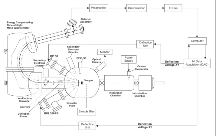
The schematic diagram of an upgraded TOF-SIMS VG Ionex IX23LS is shown in Fig. 1 and its main features are briefly summarized below. The instrument was assembled as a fully bakeable ul-tra-high vacuum (UHV) system composed of three stainless steel vessels isolated from each other by UHV gate valves and evacuated by Edwards EO4 diffusion pumps with polyphenyl ether pump-ing fluid and incorporatpump-ing CCT100 liquid nitrogen cold traps. Durpump-ing experiments the pressure in the analytical chamber is maintained at the level of (5-10)×10-8 Pa. The duoplasmatron ion-beam column has a two differential pumping stages (by a diffusion pump) and the liquid-metal ion gun, has an auxiliary 30 l.s-1 ion pump to reduce the oxygen pressure in the source’s region. We did not carry out significant modification of the vacuum system, only a resistance heated evaporator with a replaceable Cs dispenser by SAES Getters (Milan, Italy) was mounted in the preparation chamber. The vacuum is adequately clean for SIMS purposes since no significant contribution of hydrocar-bons are detected when carrying-on routine static SIMS even without the use of LN2 in the cold traps. This is certainly due to the original careful design of the vacuum system. Pressure is still is monitored by the three original ion gauges.
Positive and negative secondary ions are analyzed and detected using the energy-compensated mass spectrometer consisted of a 164.4° Poschenrieder-type analyzer [16-18] with a flight path of 2.26 m [6] and newly installed Chevron™ MA detector assembly with two microchannel plates by Photonis (Sturbridge, MA, USA). Extraction of the secondary ions is performed along the normal to the sample surface applying ± 5 kV to the sample holder; the distance between the sample surface
4
and extraction electrode is within 5-10 mm. Typical mass resolution is 300 (full width at half max-imum) and mass range is 0.5-1000 Da.
A liquid-metal ion gun MIG 300PB is used a source of analysis ions with the incident angle of 60° to the surface plane (leaving out the change of the ion-beam direction due to the accelerating-retarding field in the space between the sample surface and extraction electrode). At present, this gun is fitted with a Ga field emitter operating at up to 30 kV. The gun has condenser and focus asymmetric einzel lenses, a Wien mass filter for separation of 69Ga+ and 71Ga+ isotopes, octupole stigmators and scan rods. For continuous beam, a spatial resolution of 50-100 nm is achieved using the smallest source aperture, and with the maximum size aperture the sample current of 30 nA is obtained. In pulsed mode, auxiliary internal deflector plates chopped the ion beam producing 5-50 ns pulses with the maximal repetition frequency of 20 kHz.
We schedule to substitute pure gallium for In-Bi alloy with minor modification of the source’s construction. For In66.3/Bi33.7 the melting point is ca. 72 °C that is only slightly above the operat-ing temperature of a standard Ga source. Modified source should produce Bin+ cluster ions
improv-ing secondary ion yields of heavy molecular species [19]. We are also about to deploy room tem-perature ionic liquids [20] – molten salts characterized by melting points below 100°C - as working matter for the production of the analysis ions, in a similar way as liquid metals and alloys using field ionization. Such a source can operate in bipolar mode producing molecular ions both positive and negative polarities [21]. Recently, we have performed time-of-flight studies [22, 23] on the field evaporation of 1-alkyl-3-methylimidazolium bis(trifluoromethylsufonyl)imide, where alkyl is ethyl, butyl and hexyl, using the scanning atom probe at the Kanazawa Institute of Technology, Ja-pan. Non-degraded cationic ions at m/z 111, 139 and 167 along with positive cluster ions composed of the intact cations and anions' fragments were observed.
SIMS depth profiling is carried out in the dual beam mode [24] using a DP50B duoplasmatron gun by VG (East Grinstead, UK) for the controlled removal of the sample materials. This gun
oper-5
ates with a hollow “cold” Ni cathode producing 1-10 keV O2+ ions with the incident angle of 60° to
the sample surface. The ion-optical column contains 3 lenses (two condenser and focus), a Wien mass filter with external magnets and scan quadrupoles. The analysis and sputter ion beams are in-terlaced in the course of depth profiling. At first, 14-20 keV Ga+ pulsed beam performs the analysis with ± 5 kV potential applied to the sample. Then, during 2-5 s the sample potential is decreased to zero, and next, 2-8 keV O2+ continuous beam of 100-150 nA and 25-30 nm spot erodes the sample
surface. Usually, the sputter beam is scanned over an area of 250×250 µm2, and the analysis beam is directed to the center of sputter crater. During delay and sputter period low-and nonconductive samples can be exposed to 5-10 eV electrons for charge compensation. For that a SEG 50 low-energy electron gun by VG is used.
Physical images relating to the topographical features of the sample surface are collected either with secondary electron detector consisting of the scintillator and photomultiplier assembly fitted to the analytical chamber or with secondary ion-electron converter placed in the entrance of TOF ana-lyzer. This includes a metal plate mounted on a rotary feedthrough and another scintilla-tor/photomultiplier. A CCD camera for monitoring the sample position was recently installed in the analytical chamber.
2.2. Data acquisition and control system
The main concern in upgrading this instrument was in the acquisition system since it was fitted with a old TDC still running under Windows 95 operating system.
The schematic diagram of the newly developed data acquisition and control system is shown in Fig. 2. The system is designed around a Pentium 4 quad core computer running under Microsoft Windows7 Professional.
Two PCI based data acquisition and control interface cards are installed in this computer. A PCI-6259 by the National Instruments™ (Austin, TX, USA) contains four 16-bit analog output
6
channels with the sampling efficiency of 2.86 MS/s, thirty-two 16-bit analog input channels with the sampling speed of 1.25 MS/s, forty-eight TTL digital I/O with the maximum clock rate of 10 MHz and two 32-bit counters with plus generation capability of 10.2 ns. This card has triggering and synchronization capabilities as well. The four analog outputs are used for scanning both ion beams using custom-built XY deflection amplifiers. The analog input channels are used to read the signal from secondary electron detectors for physical imaging of the sample. Switching to continu-ous/pulsed mode and blanking/unblanking of every ion beam is carried out via a custom-built inter-face board.
A FPCI-DIO card (Fishcamp Engineering, Santa Maria, CA, USA) is used to control a TDCx4 time-to-digital converter (IONWERKS, Houston, TX, USA) and to acquire arrival time of each event previously registered by TDC. This card is a parallel digital interface for PC supporting the PCI expansion bus. It provides ninety-six TTL compatible signal lines, which may be configured in groups of eight to act as either input or output signals. Interconnection between the TDCx4 and FPCI-DIO is performed via three 50-pin ribbon cable headers on the card.
TDCx4 is a multi-channel single start multi-stop time-to-digital convertor. It accepts standard fast signals from up to four inputs simultaneously and processes them in parallel with digitizing resolution of 625 ps and a 20 ns worst case pulse pair resolution within each of the four channels. Alternatively, as in our case for the single-detector configuration, the input can be multiplexed in to the four TDC channels to increase the pulse pair resolution to 3 ns with worst case dead-time of 15 ns before the next four pulses can be encoded. Cycle time is an user-defined input through the con-trol software ranging from 2.544 to 1310 µs with 2.56 µs steps.
The secondary ions after separation by TOF analyzer are detected by a Chevron™ MA detector assembly with an electron gain of ca. 107 at 2400 V producing the pulses with a typical duration of 650 ps. The signals are amplified before passing to a model 4608C discriminator (LeCroy, Chestnut Ridge, NY, USA), which in turn is connected to TDC.
7
2.3. Software
Our dedicated software PoschTOFSIMS is developed using LabView™ 8.0 platform by Nation-al Instruments. The building blocks are virtuNation-al instruments (VIs), each designed for the specific task. These VIs can be called from the user interface and closed after accomplishment of the task.
At present, the PoschTOFSIMS can perform the following tasks: (i) acquisition of the time spec-tra with the following recalculation of the time to mass scale, (ii) sputter depth profiling in the inter-laced mode with the scanning of analysis and sputter ion beams and with charge neutralization us-ing low-energy electrons, (iii) physical imagus-ing of the sample with secondary electrons and ions (without mass separation), and (iv) chemical mapping of the sample (with mass separation of the secondary ions). For ion-beam scanning, we set our choice on the raster rectangle scheme avoiding unwanted sample erosion during each horizontal retrace used in a common TV regime. The number of pixels along X- and Y-axes is user-defined with option to select from the dropdown list. Raster rectangle mode provided good results for both physical and chemical imaging of the sample.
Ion counts are acquired from TDC in the list mode, 32 bits per stop. Data are processed and dis-played in real time with one second refreshing time, and are written to ASCII files according to ISO 22048 (2004) specifications allowing data to be analyzed by different spreadsheet analysis/plotting packages.
3. Experimental
In the frame of this work, samples were mono-crystalline semiconductor wafers fabricated in the Institute for Physics of Microstructures, Russian Academy of Science (N. Novgorod). They are conducting at room temperature (RT) due to the slightly n-type doping in the range of 1016-1018 cm
-3 and can be considered as non-degenerated semiconductors. As the electron work function of
thermo-8
dynamic work function φ are usually employed. The electron affinity is the work needed to transfer an electron from the bottom of conduction band to the vacuum level with zero kinetic energy, and the thermodynamic work function means about the same as in the case of metals. However, for semiconductors, as opposite to metals, there are no electrons on the Fermi level locating into band-gap; moreover, the energy position of this level depends on the temperature, on the type, concentra-tion, degree of degeneracy and other details of the dopants [25]. In some works, the threshold ener-gy of external photoelectric effect ET is also considered as the electron work function of semicon-ductors.
The χ- , φ - and ET -values of non-degenerated III-V semiconductors are presented in Table 1. For gallium phosphide, only the value of electron affinity was found in literature. Other important parameters for interpretation of our experimental results are the electron affinity A of non-metallic (V group) atoms and Pauling electronegativity EN of all atoms composing III-V semiconductors [30]; these values are summarized in Table 2.
For the TOF-SIMS analysis of negative secondary ions we used Ga+ primary ions of 19 keV
impact energy (14 keV of own bombarding energy plus 5 keV due to the acceleration by the nega-tive sample potential). The mass spectra were acquired within 1 min interval with 6 kHz pulsed beam scanned across a rectangular area of ca. 200×125 µm2 placed in the center of the sputter area. The sputtering of the sample surface was performed using the same beam in the continuous mode with the sample current of 5 nA over a 750×500 µm2 area.
Cesium vapor deposition was carried out in the preparation chamber at 5×10⁻⁷ Pa. We used care-fully outgassed getter dispenser and deposited approximately the same amount of Cs on the surface of every sample. We did not measure the deposition rate, however due to the low sticking efficiency of Cs onto other Cs atoms the thickness of the deposited films can be estimated within a few mono-layers. After the deposition, the samples were immediately transferred to the analytical chamber under UHV conditions.
9
4. Results and discussion
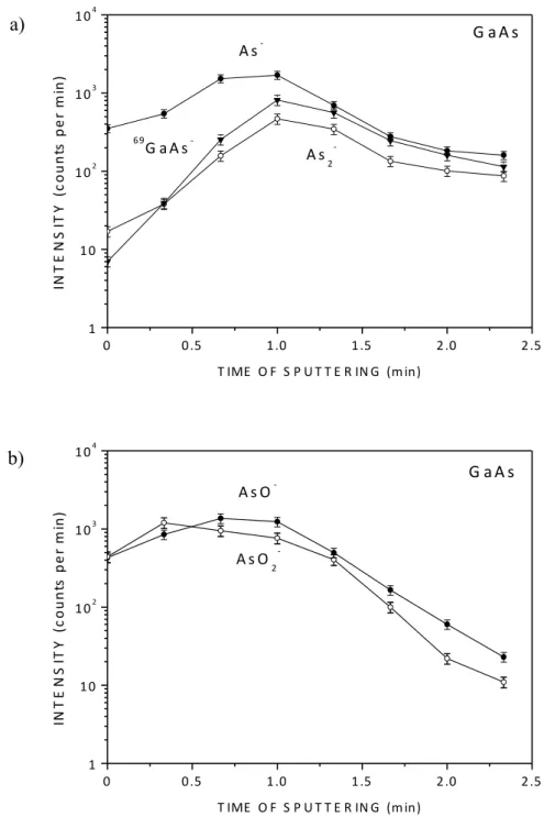
In this section we give a detailed account of the experimental results obtained for GaAs. In Fig. 3 the mass spectra of the positive secondary ions before and after Cs deposition are presented in the histogram form with the peak intensities integrated within ± 0.5 m/z. For the as-received sample, besides Ga isotopes the low-intense peaks of alkali metals and Ga oxides were registered; arsenic and As-containing positive ions were not detected at the level of sensitivity of our instrument since the As+ yield for III-V semiconductors with Ga+ ion-beam bombardment is very low. After Cs dep-osition only Cs+ peak is presented in the spectrum (the gray line in Fig. 3).
The mass spectra of the negative secondary ions (not shown) were more complex with intense peaks of H-, O-, OH- and some hydrocarbons; however, the intensity of atomic and molecular
As-containing negative ions for the as-received sample continued to be low.
Fig. 4 shows the intensities of these ions versus the time of Ga+ ion-beam bombardment of the GaAs sample with prior Cs deposited layers. Similar plots were obtained for other III-V semicon-ductors. To explain these dependencies, we need to factorize the peak intensity I. In the first ap-proximation for singly-charged atomic secondary ions it can be presented as
𝐼 ∝ 𝑌 ∙ 𝛽!∙ 𝐶, (1)
where Y is the partial sputter yield, i.e. the average number of atoms of a species ejected from the sample per incident ion, β- is the negative ionization probability, i.e. the fraction of the sputtered flux of a species that is ionized, and C is the relative atomic concentration of a species.
The influence of cesium over and sub-surface layers on the ionization probability of secondary ions has long been studied and still continues to be a subject of intense research (for a review see, e.g. [31, 32] and the references cited in Introduction). It is established that lowering the electron work function by Cs0 deposition or Cs+ implantation always suppresses the emission of positive ions and, at the same time, enhances the negative ion yields for both metallic and semiconducting
10
substrates. According to the electron-tunneling model [31], the negative ionization probability β -depends on the work function Φ as follows
𝛽! ∝ 𝑒𝑥𝑝 −!!!
!! , (2)
where A is the electron affinity and εn is the system specific parameter depending on the energy and emission angle of sputtered. This equation is valid if Φ >A, otherwise if Φ ≤ A, β- =1.
It is known (see, e.g. [31-33]) that surface adsorption of cesium atoms results in the charge transfer to the substrate. This interaction is mainly of covalent manner, especially in the case of semiconductors, and Cs adatoms generate the long-ranged electrostatic dipole field, which reduces the work function of the substrate. This change is different for metals and semiconductors. Using angle-resolved ultraviolet photoelectron spectroscopy and medium energy ion scattering, Heskett et al. [33] found that for n-type GaAs (110) at RT the Cs-induced work function decrease ΔΦ saturates at ca. 3.6 eV for the Cs surface concentration of 4×10¹⁴ at.cm-2. This is almost one monolayer cov-erage, and the minimal value of the work function for GaAs with such Cs coverage was estimated as 1.7 eV, i.e. starting value was ΦGaAs= 5.3 eV. This value is closer to the threshold energy of
ex-ternal photoelectric effect of non-degenerated GaAs [25] than to the exex-ternal or thermodynamic electron work function of GaAs presented in Table 1 [25, 26]. The adsorption of a second and next Cs layers leads to the formation of metallic film with the work function of pure Cs, which is 2.14 eV [30]. Such a behavior is typical for other alkali metal-semiconductor systems [33].
We can propose that the main changes in the peak intensities shown in Fig. 4 are due to the changes in the ionization probability relating to the modification of electron work function of the sample. For the starting point of the plots shown in Fig. 4, the Φ -value is approximately the same as of metallic Cs because a few Cs layers were deposited. However, it is lower than the work func-tion of pure GaAs. Then the Cs layers began to be removed by Ga+ primary ions and after ca. 40-60 s the intensity of the As-containing secondary ions maximized (Fig. 4a). Presumably, at this time
11
the Cs monolayer coverage allowing for the minimal work function of the sample was reached. Ac-cording to Eq. (2), to the lowest value of the difference (Φ - A) should correspond to the highest ionization probability, i.e. the greatest peak intensity. The rest of Cs layer continued to be sputtered, and the work function of the system increased and eventually became the same as of pure GaAs.
This is a simplified scenario taking into account the main processes influencing the dependen-cies presented in Fig. 4. Using experimental data, we estimated the thickness of the sputtered Cs layers. The sputter rate Vsp (in nm.s-1) can be calculated as
𝑉!" ≈ 10!! !∙!∙!!
! , (3)
where M is the mass of sputtered atoms (MCs = 133 Da), ρ is the mass density (ρCs = 1.93 g.cm-3 [30]), Y is the sputter yield (at our experimental conditions YCs ~ 5-7 at.ion-1 [34]), j0 is the density of primary ion beam (j0 =1.3 µA.cm-2). We obtained Vsp ~ 5.10-2 nm.s-1; it means that for 40-60 s we were able to sputter 6-10 monolayers assuming that the thickness of Cs monolayer is 0.3 nm [30]. This is only rough estimate because the Cs films could be grossly inhomogeneous. The sputter effi-ciency of the pulsed Ga+ beam was negligible since the Ga+ current density in the analysis (pulsed) mode a five hundred times lower than in the sputter (continuous) mode.
Ion-beam sputtering is usually accompanied by implantation of bombarding ions, surface roughness formation, ion-induced diffusion and segregation, ballistic mixing and radiation defects production, etc. (see, e.g. [35] and references cited therein). For multicomponent systems the pref-erential sputtering can occur as well. All these processes are complex and hardly analyzable; their detailed discussion is beyond the scope of our paper.
Using SRIM-2008.04 code [36] we calculated the depth profile and relative atomic concentra-tion of Ga atoms implanted in GaAs covered with 5 and 10 surface monolayers of Cs. The results of our calculations for 10 monolayers coverage are presented in Fig. 5. The ion average range (the av-erage penetration depth) was estimated as 12.6 nm and 13.5 nm for 5 and 10 monolayers, respec-tively, and the maximal Ga concentration was within 1.5 at. % for both coverage’s values.
Accord-12
ing to our calculations, the number of Cs recoils knocked into the substrate by Ga+ primary ions was negligible.
The information concerning preferential sputtering in III-V semiconductors is scant and contra-dictory, especially in case of Ga+ ion-beam bombardment. It was found [37] that upon low-energy Ar+ sputtering (the mass of those are close to Ga ions) the surface of GaAs is enriched with Ga
at-oms, but to a very little degree. For other III-V semiconductors both components could prevail on the surface, but again by a negligible margin. In general, surface roughness formation under ion-beam bombardment is of importance for III-V semiconductors; however, in our case it was rather small due to the short duration of our experiments.
To sum up the above, we inferred the insignificance or very little influence of the ion-induced perturbing effects, of course, under our experimental conditions on the sputter yield Y and relative atomic concentration C of the electronegative elements (P, As and Sb) composing III-V semicon-ductors. According to Eq. (1), the changes in the peak intensities I shown in Fig. 4 can be interpret-ed in terms of the ionization probability β- depending via Eq. (2) on the changing of the electron work function Φ of the system or more correctly on the difference (Φ - A), where A is the electron affinity of the sputtered atoms.
Till now, we have been speaking about atomic ions. The plots for As2 and GaAs negative
sec-ondary ions presented in Fig. 4a look similar to those measured for As ions. We can suppose that the efficiency of dimer and cluster ion formation depends on the intensity of atomic ions, and the main processes governing the atomic ion production can be valid for the polyatomic ions as well.
The data for As-containing oxides ions shown in Fig. 4b deserve more detailed discussion. It is known that oxygen atoms and molecules adsorbed on the surface of III-V semiconductors exhibit very strong acceptor behavior. During Cs deposition, oxygen can interact with cesium and form Cs2O, increasing the dipole field per unit of area, which eventually leads to extra decreasing of the
13
At present, cesium ion sputtering with oxygen flooding has been studied with a great attention [38-41]. It was found that even a very small partial pressure of oxygen (in the 10-7 to 10-6 Pa range) quite strongly influences the negative ion emission and sputter yields of the cesiated silicon surface. Our experiments were carried out at total residual pressure of 10-7 Pa, and we roughly estimated the partial oxygen pressure to be hundred times lower. We did not detect any negative or positive Cs oxides secondary ions after cesium deposition. It means that oxygen adsorption during Cs depo-sition resulting in CsO2 formation was small or negligible. At the same time, natural oxides
present-ed on the surface of our samples and their negative ion yields also enhancpresent-ed after the surface cesia-tion in a similar manner as for atomic ions of V-group elements. When the Cs coverage was re-moved by Ga+ sputtering, the intensities of AsO and AsO
2 ions decreased in a greater extent as
against the intensities of As, As2 and GaAs ions (see Fig. 4 and Table 3). We believe that Ga+
ion-beam sputtering cleaned the surface of GaAs, i.e. effectively decreased the surface concentration of arsenic (gallium) oxides, especially when Cs layers were fully eroded.
To quantify the increase in the peak intensities of different ion species emitted from different semiconductors after the surface cesiation, we introduce the ion signal enhancement K that is the ratio of the maximal to minimal peak intensities. The K-values calculated for all III-V semiconduc-tors studied in this work under identical experimental conditions are listed in Tables 3-5. The data accuracy was within 15-20 %.
To analyze the experimental data shown in Fig. 4 and presented in Tables 3-5, one can find out the following trends:
1) the K-factors of any similar secondary ion species (atomic, dimer, cluster and oxides) are bigger for In-based compounds as against Ga-based ones;
2) for every sample, the K-factor of monoatomic ions is bigger than in case of dimer and clusters; the greatest value (360) was obtained for phosphorus secondary ions emitted from InP;
14
3) for oxides secondary ions, the K-factor of molecular ions containing two oxygen atoms is bigger than for monoxide ions (excepting GaSb); the greatest value (1790) was obtained for PO2- ions
emitted from InP.
Using Eq. (1) and (2), we can estimate that 𝐾 = !!"#
!!"# ∝ 𝑒𝑥𝑝
∆!
!! , (4)
where ΔΦ =Φmax -Φmin is the Cs-induced decrease of the electron work function, i.e. the difference of work functions before and after cesiation with optimal (monolayer) Cs coverage.
The estimate of absolute value of ΔΦ for different III-V semiconductors is a hard problem, however, from the experimental results presented in Tables 3-5 we can propose that for In-based compounds ΔΦ is bigger than in case of Ga-based. According to Eq. (4), the K-factor does not de-pend on the electron affinity of sputtered atoms, but only if sputter yield Y and εn parameter remain the same for initial and Cs-covered surfaces.
To proceed with K-factor discussion, we does not scale its values presented in Tables 3-5 nei-ther with electron affinity A of V-group atoms (see Table 2) nor with the difference (Φ - A) using as Φ -value true or thermodynamic work functions or threshold energy of external photoelectric effect listed in Table 1.
Some correlation of our experimental results with the difference in Pauling electronegativity ΔEN =│ENV - ENIII│, where ENV and ENIII is the electronegativity of V-group (P, As and Sb) and III-group (Ga and In) components of semiconductors, respectively, can be revealed. In general, the greater the difference in electronegativity between two atoms formed molecule or compound, the more polar the bond generated between them. Long ago, Šroubek [42] demonstrated that As- ion
yield upon Ar+ ion-beam bombardment bigger for InAs as against GaAs, both for clean and Cs-covered surfaces. He explained that in terms of the bond polarity (ionicity) of these compounds; ac-tually, ΔENInAs >ΔENGaAs (see Table 3).
15
The ΔEN-values are presented in Tables 3-5 along with the experimental data of ion signal en-hancement K. In principle, instead of Pauling estimates other electronegativity scales like Mulliken-Jaffe, Allred-Rochow, Sanderson, etc. [30] can be used; it does not change fact of matter. One can see that of all In-based semiconductors the bond ionicity is greater than of the corresponding Ga-based compounds. It means that for In-Ga-based semiconductors the electrostatic dipole field produced by Cs adatoms stronger and the work function ΔΦ decrease greater than for Ga-based ones. From this position, the biggest ion signal enhancement obtained for P-containing secondary ions can be explained to the bigger electronegativity difference of GaP (InP) semiconductors as against others. At the same time, the electronegativity concept does not answer why K-factor of Sb-containing ion species are higher than of As ones, despite ΔENGaAs(InAs) >ΔENGaSb(InSb). This can be a subject to fu-ture research.
5. Conclusion
A detailed experimental study on the influence of prior neutral cesium deposition on the sec-ondary emission of negative atomic and cluster ions of non-metallic elements (P, As and Sb) upon 19 keV Ga+ bombardment of non-degenerated III-V semiconductors (GaP, GaAs, GaSb, InP, InAs and InSb) was carried out using a TOF-SIMS VG Ionex IX23LS upgraded in our lab. Our purpose was twofold: first, to examine the applicability of our TOF-SIMS with newly developed data acqui-sition and control system for systematic fundamental research, and as a consequence, to explore un-der identical experimental conditions how the enhancement of negative secondary ion yields of V-group atoms depend on physicochemical characteristics (electron work function, electron affinity, electronegativity) of III-V semiconductors and individual atoms composing these materials.
The main experimental results can be summarized as follows:
(1) After the surface cesiation, the ion signal enhancement (K-factor) of any negative species (atomic, dimer, clusters and oxides) was bigger for In-based compounds as against Ga-based ones. We explain that in terms of the electronegativity difference between atoms composing
16
III-V semiconductors. The greater electronegativity difference (bond ionicity) of In-based compounds results in the greater Cs-induced work function decrease that leads to the bigger increase in the ionization probability of secondary ions (their peak intensities).
(2) For every sample studied, the K-factor of monoatomic ions was bigger than in case of dimer and clusters; the greatest value (360) was obtained for phosphorus secondary ions emitted from InP. It means that the efficiency of dimer and cluster ion formation depends on the in-tensity of atomic ions.
(3) For O-containing negative secondary ions, the K-factor of molecular ions with two oxygen atoms was bigger than of monoxide ions (excepting GaSb); the greatest value (1790) was obtained for PO2- ions emitted from InP. We are of opinion that the sputtering of surface
ox-ides mainly contributed to this type of ion emission, and double oxox-ides could be prevalent natural oxides for V-group atoms.
From the practical point of view, neutral cesium deposition onto the sample surface prior to the static SIMS analysis can be considered as a very useful adjunct for the detection of electronegative species, especially, for the chemical (elemental) visualization of the first monolayers with higher sensitivity as against standard SIMS.
Moreover, the upgraded Tof-SIMS instrument has shown to be adequate for further use in rou-tine and research analyses. The limitation of the previous control and data acquisition system was overcame resulting in a user-friendly, and still powerful, surface analysis facility.
Acknowledgments
This study was carried out in the framework of the Ciencia 2009 Program by FCT, Portugal. We thank M. Drozdov for III-V semiconductor samples kindly presented for our investigation. We are also very grateful to B.-J Shaw for careful English editing of our manuscript.
17
References
[1] A. Benninghoven, The development of SIMS and international SIMS conferences: a personal retrospective view, Surf. Interface Anal. 43 (2011) 2-11.
[2] A. J. Eccles, T. A. Steele, A. W. Robinson, Broadening the horizons of SIMS: the low cost Chemical Microscope, Appl. Surf. Sci. 144-145 (1999) 106-112.
[3] A. Tolstogouzov, S. F. Belykh, M. Stepanova, S. K. Dew, C. Pagura, Characterization of Al+ secondary ion emission produced by Ne+ and Ar+ bombardment of aluminum surface, Surf. Rev.
Lett. 11 (2004) 391-401.
[4] U. Bardi, S. P. Chenakin, F. Ghezzi, C. Giolli, A. Goruppa, A. Lavacchi, E. Miorin, C. Pagura, A. Tolstogouzov, High-temperature oxidation of CrN/AlN multilayer coatings, Appl. Surf. Sci. 252 (2005) 1339-1349.
18
[6] A. R. Waugh, D. R. Kingham, C. H. Richardson, M. Coff, A time-of-flight mass spectrometer for SIMS and field ionized neutral analysis using a pulsed LMIS, J. Physique Coll. 48 (1987) C6: 577-582.
[7] K. Wittmaack, Secondary ion yield variations due to cesium implantation in silicon, Surf. Sci. 126 (1983) 573-580.
[8] H. Gnaser, Exponential scaling of sputtered negative-ion yields with transient work-function changes on Cs+-bombarded surfaces, Phys. Rev. B 54 (1996) 16456-16459.
[9] T. Wirtz, B. Duez, H.-M. Migeon, H. Scherrer, Useful yields of MCs+ and MCs2+ clusters: a
comparison study between the Cameca IMS 4f and the Cation mass Spectrometer, Int. J. Mass Spectrom. 209 (2001) 57-67.
[10] V. E. Krohn, Emission of negative ions from metal surfaces bombarded by positive cesium ions, J. Appl. Phys. 22 (1962) 3523-3526.
[11] P. Philipp, T. Wirtz, H.-M. Migeon, H. Scherrer, SIMS analysis with neutral cesium deposition: Negative secondary ion sensitivity increase and quantification aspects, Int. J. Mass Spectrom. 253 (2006) 71-78.
[12] P. Philipp, J.-N. Audinot, T. Wirtz, H.-M. Migeon, Neutral cesium deposition prior to SIMS analysis of organic and inorganic samples, Surf. Interface Anal. 42 (2010) 1499-1506.
[13] R. Said, N. Ali, C. A. A. Ghumman, O. M. N. D. Teodoro, W. Ahmed, Characterization of DLC films deposited using titanium isopropoxide (TIPOT) at different flow rates, J. Nanosci. Nanotech-nol. 9 (2009) 4298-4304.
[14] C. A. A. Ghumman,O. M. T. Carreira,A. M. C. Moutinho, A.Tolstogouzov,V. Vassilenko, O. M. N. D. Teodoro, Identification of human calculi with time-of-flight secondary ion mass spec-trometry, Rapid Comm. Mass Spectrom. 24 (2010) 185-190.
19
[15] C. A. A. Ghumman,A. M. C. Moutinho, A.Tolstogouzov,O. M. N. D. Teodoro, Time-of-flight secondary ion mass spectrometric identification of calcium formate Ca(HCO2)2 and metabolite of
vitamin B6 in human stones, Rapid Comm. Mass Spectrom. 25 (2011) 997-999.
[16] W. P. Poschenrieder, Multiple-focusing time of flight mass spectrometers. Part I. TOFMS with equal momentum acceleration, Int. J. Mass Spectrom. Ion Phys. 6 (1971) 413-426.
[17] W. P. Poschenrieder, Multiple-focusing time of flight mass spectrometers. Part II. TOFMS with equal energy acceleration, Int. J. Mass Spectrom. Ion Phys. 9 (1972) 357-373.
[18] G.-H. Oetjen, W. P. Poschenrieder, Focusing errors of a multiple-focusing time-of-flight mass spectrometer with an electrostatic sector field, Int. J. Mass Spectrom. Ion Phys. 16 (1975) 353-367. [19] F. Kollmer, Cluster primary ion bombardment of organic materials, Appl. Surf. Sci. 231-232 (2004) 153-158.
[20] T. Welton, Room-temperature ionic liquids. Solvents for synthesis and catalysis, Chem. Rev. 99 (1999) 2071-2083.
[21] P. C. Lozano, Energy properties of an EMI-Im ionic liquid ion source, J. Phys. D: Appl. Phys. 39 (2006) 126-134.
[22] A. Tolstogouzov, U. Bardi, O. Nishikawa, M. Taniguchi, Study on imidazolium-based ionic liquids with scanning atom probe and Knudsen effusion mass spectrometry, Surf. Interface Anal. 40 (2008) 1614-1618.
[23] A. Tolstogouzov, U. Bardi, O. Nishikawa, M. Taniguchi, Mass spectrometric analysis of imid-azolium-based ionic liquids by scanning atom probe, Int. J. Mass Spectrom. 281 (2009) 37-40. [24] T. Grehl, R. Mollers, E. Niehuis, Low energy dual beam depth profiling: influence of sputter and analysis beam parameters on profile performance using TOF-SIMS, Appl. Surf. Sci. 203-204 (2003) 277-280.
[25] K. V. Shalimova, Physics of Semiconductors, Energiya, Moscow, 1976 (in Russian). [26] Available (2011): http://www.ioffe.rssi.ru/SVA/NSM/Semicond/index.html
20
[27] P. Andersson, A. O. Lindahl, C. Alfredsson, L. Rogström, C. Diehl, D. J. Pegg, D. Hanstorp, The electron affinity of phosphorous, J. Phys. B 40 (2007) 4097-4107.
[28] C. W. Walter, N. D. Gibson, R. L. Field, III, A. P. Snedden, J. Z. Shapiro, C. M. Janczak, D. Hanstorp, Electron affinity of arsenic and the fine structure of As− measured using infrared photo-detachment threshold spectroscopy, Phys. Rev. A 80 (2009) 014501 (1-4).
[29] M. Scheer, H. K. Haugen, D. R. Beck, Single- and multiphoton infrared laser spectroscopy of
Sb-: A case study, Phys. Rev. Lett. 79 (1997) 4104-4107.
[30] Available (2011): http://www.webelements.com/
[31] M. L. Yu, Charged and excited states of sputtered atoms, in: R. Behrisch, K. Wittmaack (Eds.), Sputtering by Particle Bombardment III. Characteristics of Sputtered Particles, Technical Applica-tions, Springer, Berlin, 1991, pp. 91-160.
[32] Y. Kudriavtsev, R. Asomoza, Work function change caused by alkali ion sputtering of a sam-ple surface, Appl. Surf. Sci. 167 (2000) 12-17.
[33] D. Heskett, T. Maeda Wong, A. J. Smith, W. R. Graham, N. J. DiNardo, E. W. Plummer, Cor-relation of alkali metal-induced work function changes on semiconductor and metal surfaces, J. Vac. Sci. Technol. B 7 (1989) 915-918.
[34] L. A. Giannuzzi, F. A. Stevie (Eds.), Introduction to Focused Ion Beams. Instrumentation, Theory, Techniques and Practice, Springer, New York, 2005.
[35] H. W. Werner, P. R. Boudewijn, Depth profiling using sputtering methods, in: A. W. Czander-na, T. E. Madey, C. J. Powell (Eds.), Beam Effects, Surface Topography, and Depth Profiling in Surface Analysis, Plenum Press, New York, 1998, pp. 355-420.
[36] Available (2011): http://www.srim.org/
[37] G. Betz, G. K. Wehner, Sputtering of multicomponent materials, in: R. Behrisch (Ed.), Sputter-ing by Particle Bombardment II. SputterSputter-ing of Alloys and Compounds, Electron and Neutron Sput-tering, Surface Topography, Springer, Berlin, 1983, pp. 12-90.
21
[38] A. Merkulov, E. de Chambost, M. Schuhmacher, P. Peres, Toward accurate in-depth profiling of As and P ultra-shallow implants by SIMS, Appl. Surf. Sci. 231-232 (2004) 640-644.
[39] Y. Kudriatsev, A. Villegas, S. Gallardo, G. Ramirez, R. Asomoza, V. Mishurnuy, Cesium ion sputtering with oxygen flooding: Experimental SIMS study of work function change, Appl. Surf. Sci. 254 (2008) 4961-4964.
[40] K. Franzreb, P. Williams, Negative ion yield and sputter yield variations for Cs+ bombardment of Si with O2 gas flooding, Surf. Interface Anal. 43 (2011) 129-133.
[41] B. Berghmans, J. Rip, W. Vandervorst, Cesium retention during sputtering with low energy Cs+ and oxygen flooding, Surf. Interface Anal. 43 (2011) 225-227.
[42] Z. Šroubek, Ionization of atoms sputtered from AIIIBV compounds, Nucl. Instrum. Meth. Phys.
Res. 218 (1983) 336-339.
Captions
Fig. 1. Schematic view of the upgraded TOF-SIMS VG Ionex IX23LS.
Fig. 2. Schematic diagram of the newly developed data acquisition and control system.
Fig. 3. Mass spectra of the positive secondary ions measured for GaAs before (black) and after (gray) Cs deposition.
Fig. 4. Intensity of the negative secondary ions emitted from GaAs after Cs deposition versus the time of Ga+ ion-beam sputtering: a) As-containing atomic and cluster ions, b) As oxides ions.
Fig. 5. Relative atomic concentration of Ga implanted in GaAs covered with 10 surface monolayers of Cs. The calculations were carried out using SRIM-2008.04 code. Input data: 19 keV Ga+ ions with the incident angle 60° to the surface plane, the total ion flux FGa = 1015 cm-2.
22
23
25
Fig. 3. Mass spectra of the positive secondary ions measured for GaAs before (black) and after (gray) Cs deposition 0 50 100 150 200 1 10 102 103 104 105 106 Cs Ga2O Ga2 Ga GaO IN T E N S IT Y ( co u n ts p e r min ) m/z GaAs K, Ca
26 0 0.5 1.0 1.5 2.0 2.5 1 10 102 103 104 A s O -A s O2 -IN T E N S IT Y ( co un ts p er m in ) T IME O F S P U T T E R IN G (min) G a A s
Fig. 4. Intensity of the negative secondary ions emitted from GaAs after Cs deposition versus the time of Ga+ ion-beam sputtering: a) As-containing atomic and cluster ions, b) As-oxides ions.
0 0.5 1.0 1.5 2.0 2.5 1 10 102 103 104 69 G a A s- A s 2 -IN T E N S IT Y ( co un ts p er m in ) T IME O F S P U T T E R IN G (min) G a A s A s -a) b)
27
Fig. 5. Relative atomic concentration of Ga implanted in GaAs covered with 10 surface monolayers of Cs. The calculations were carried out using SRIM-2008.04 code. Input data: 19 keV Ga+ ions with the incident angle 60° to the surface plane, the total ion flux FGa = 1015 cm-2.
0 20 40 60 80 100 0 0.5 1.0 1.5 2.0 C Ga (at .% ) D E P T H (nm) C s (10 m onola yers )
G a A
s
28
Table 1
Electron affinity (true or external electron work function) [26], thermodynamic electron work func-tion [25] and threshold energy of external photoelectric effect [25] of non-degenerated III-V semi-conductors (at RT)
Ga-based compounds In-based compounds GaP GaAs GaSb InP InAs InSb
Electron affinity χ (eV) 3.8 4.07 4.06 4.38 4.9 4.59
Thermodynamic work function φ (eV) - 4.71 4.76 4.45 4.9 4.75 Threshold energy of external photo effect ET (eV) - 5.47 4.76 5.68 5.31 4.77
29
Table 2
Electron affinity [27-29] and Pauling electronegativity [30] of the individual atoms composing III-V semiconductors studied in this work
Ga In P As Sb
Electron affinity A (eV) - - 0.75 [27] 0.81 [28] 1.05 [29] Pauling electronegativity EN 1.81 1.78 2.19 2.18 2.05
30
Table 3
Increase in the negative secondary ion peak intensities of GaP and InP after Cs deposition; ΔEN is the electronegativity difference between Ga (In) and P atoms
Compound ΔEN
Ion signal enhancement K
P P2 PO PO2 PO3 69GaP 115InP
GaP 0.38 34 14 45 110 73 32 - InP 0.41 360 73 233 1790 177 - 242
31
Table 4
Increase in the negative secondary ion peak intensities of GaAs and InAs after Cs deposition; ΔEN is the electronegativity difference between Ga (In) and As atoms
Compound
ΔEN
Ion signal enhancement K
As As2 AsO AsO2 69GaAs 115InAs
GaAs 0.37 14 6 60 140 9 -
32
Table 5
Increase in the negative secondary ion peak intensities of GaSb and InSb after Cs deposition; ΔEN is the electronegativity difference between Ga (In) and Sb atoms
Compound ΔEN
Ion signal enhancement K
121Sb 121Sb
2 121SbO 121SbO2 69Ga121Sb 115In121Sb
GaSb 0.24 20 3.5 13.5 8 3.7 -