Spray Deposited Nanostructured CuO Thin Films: Influence of Substrate Temperature and
Annealing Process
Hassan Zare Asla,b, Seyed Mohammad Rozatia*
Received: August 23, 2017; Revised: October 29, 2017; Accepted: December 04, 2017
In this study, CuO thin films were deposited on glass substrates at a wide range of temperatures from 450ºC to 550ºC with steps of 25ºC by chemical spray pyrolysis technique. Aiming to investigate the effect of annealing process, one of the resulting films was annealed at 450ºC for 3 hours under ambient air. Based on X-ray diffraction, all the resulting films are monoclinic with two prominent peaks at ~36º and ~39º. The crystallite size of the CuO film deposited at 450ºC was found to be the largest in comparison with the others. As the substrate temperature increased, a gradual change was observed for the CuO thin film surface morphology and in the case of annealed film, the grains and their boundaries became indistinguishable. The resistivity of the films was reduced by virtue of increasing the substrate temperature and also, both the mobility and carrier concentration of the annealed film were improved drastically after annealing. As expected, the CuO thin films absorption was considerable in the visible region and gradually declined after 800nm. The estimated band gap value of the CuO film deposited at 450ºC were fairly close to the optimum band gap for solar applications.
Keywords: CuO thin film, spray pyrolysis technique, substrate temperature, annealing process.
*e-mail: [email protected]
1. Introduction
Solar cell technology is one of the promising technologies, which has been the main focus of attention in the last decades and yet it demands more study to make it more cost-effective and therefore competitive with the conventional sources of energy. Among the active layers which have thus far been used in solar cells, cupric oxide (CuO) has recently received a lot of critical attention. Apart from a rather high theoretical conversion efficiency 1, abundance and nontoxicity make CuO thin film a wise choice for solar applications 2.
CuO with its monoclinic structure naturally exhibits p-type conductivity and the band gap values of 1.3-2.1 eV has been reported in literatures 3. The possibility of depositing CuO with almost all conventional methods, such as sputtering 4, sol-gel 5, chemical vapor deposition 6, thermal deposition 7, can provide the groundwork for the deposition of CuO films with a wide variety of characteristics. However, the main drawback of the most sophisticated methods is the fact that they require highly expensive devices and processes. In comparison, chemical spray pyrolysis is a non-vacuum and solution-based technique along with suitability for mass production, which makes it a more convenient and less expensive method for thin film deposition 8.
One can deposit almost all the oxide semiconductors by adjusting the spray deposition parameters such as precursor
properties 9, substrate temperature 10, flow rate 11, nozzle-substrate distance 12, etc. Among the spray deposition parameters, the substrate temperature and annealing temperature are the most
common parameters optimized to obtain a thin film with desirable features. In the last decade, there has been several studies in which the influence of aforementioned factors has been investigated 13,14; yet in this study, CuO thin films have been deposited in high substrate temperatures starting from 450ºC and finishing at 550ºC in which the deposition rate declines drastically. It was found that, up to 525ºC, as the substrate temperature increases, the resistivity of the resulting CuO thin films decreases and again it increases for the film deposited at 550ºC. Furthermore, with the purpose of studying the influence of annealing process, one of the deposited films was annealed. Finally, the structural, morphological, electrical, and optical properties of the resulting films have been studied.
2. Experimental
Nanostructured CuO thin films were deposited on well-cleaned glass substrates via spray pyrolysis. Precursors were prepared by dissolving appropriate amount of Copper (II) chloride dehydrate in deionized water to obtain a starting solution with 0.05M molarity. The resulting solution was sprayed by a homemade spray apparatus with a custom class gun having a nozzle diameter of 0.2mm. In order to deposit each film, 0.9bar filtered air was applied to the nozzle positioned at 29cm above the substrate with the substrate temperature varying from 450ºC to 550ºC with steps of 25ºC. The optimized experimental conditions of spray deposition have been given in Table 1. Finally, with the purpose of studying the influence of the annealing process, the film deposited at 500ºC was also annealed at 450ºC for 3 hours. aDepartment of Physics, University of Guilan, Rasht, Iran
The structure of the abovementioned deposited CuO thin films were studied by Grazing Incident X-ray diffraction (GIXRD) (X’Pert PRO MPD model) with Cu-Kα radiation. A surface profilometer (Bruker Dektak XT1) was applied to measure as-prepared steps on the surface of the CuO films. The surface morphology was examined by a field emission scanning electron microscopy (FESEM) (JEOL JSM-7610F) and atomic force microscopy (AFM) (FemtoScan SPM). The Hall Effect measurements (Phys Tech) were performed
on 7×7 mm2 CuO thin films using 0.56T magnetic field in room temperature. The Van der Pauw contacts (coplanar) geometry was employed for all measurements. Electrical contacts were made to each of the four corners with silver paste. Optical transmittance, absorbance and reflectance of the resulting films were recorded by means of an UV-vis spectrometer (Perkin-Elmer Lambda 25).
3. Results and Discussion
3.1. Structural properties
Fig. 1 shows the grazing incident X-ray diffraction (GIXRD) of the CuO thin films prepared at different substrate temperatures via spray pyrolysis technique. All the deposited films are polycrystalline with a monoclinic crystal structure, and there is no trace of the other common phase of copper oxide (Cu2O). There are two prominent peaks at ~36º and ~39º which can be well indexed to the monoclinic CuO (JCPDS Card No. 045-0937)15-17.
In order to study the influence of substrate temperate on the structural properties of the deposited films, the mean crystallite size (D) was estimated for two preferential orientations of the resulting films using the Scherrer’s equation:
(1)
where λ is the wavelength of the X-rays, β is the full width at half-maximum (FWHM) of diffraction peaks (in radians), and θ is the Bragg’s diffraction angle 18. The results have been
listed in Table 2, and the variation of the mean crystallite size for the two major peaks along with the intensities of the aforementioned peaks has been shown in Fig. 2.
One can see that the largest crystallite grows up at the substrate temperature of 450ºC and gradually decreases as the substrate temperature increases. However, there is a slight increase in the crystallite size of the film deposited at the substrate temperature of 550ºC compared with 525ºC which might be attributed to the lower rate of deposition in a high temperature, resulting in a larger crystallite size. Annealing the as-deposited layer at 500ºC led to an increase in the crystallite size; yet, it was still lower than the mean crystallite size of the as-deposited film at the substrate temperature of 450ºC.
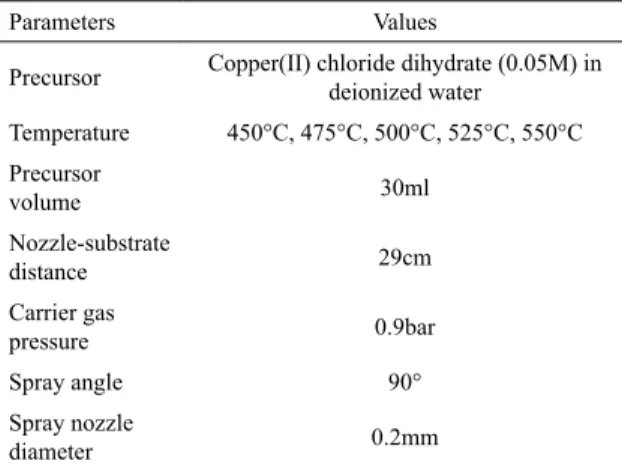
Furthermore, the lattice parameters (a≠b≠c, α=γ=90º≠ β) and unit cell volume (V) of CuO thin films have been calculated from the following equations:
(2)
(3)
where a, b, c and β are the lattice parameters for the monoclinic structure, (h k l) are the Miller indices and d is the interplanar distance 19. The results have been shown in Table 3.
3.2. Morphological properties
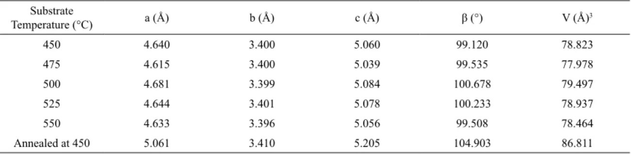
The surface micrographs of the CuO thin films deposited at 450ºC, 500ºC, and 550ºC have been shown in Fig. 3a-c, respectively. The surface morphology of these films exhibits a random grain distribution on the surface with mainly trapezium grain shapes. The estimated mean grain sizes for the CuO films have been shown in Table 4. As can be seen, the mean grain size increases from 138nm for
Table 1. Optimized experimental parameters of the spray deposition.
Parameters Values
Precursor Copper(ΙΙ) chloride dihydrate (0.05M) in deionized water
Temperature 450°C, 475°C, 500°C, 525°C, 550°C Precursor volume 30ml Nozzle-substrate distance 29cm Carrier gas pressure 0.9bar
Spray angle 90°
Spray nozzle
diameter 0.2mm
.
cos
D
=
b
0 94
m
i
sin sin cos d a h b k c l ac hl
1 1 2
2 2 2
2 2 2 2 2 2 b b b
= T + + - Y
sin
V
=
abc
b
Figure 1. GIXRD pattern of the as-deposited CuO thin films at
Table 2. Thickness and calculated crystallite size of the CuO thin films deposited at different substrate temperatures and the CuO thin film annealed at 450°C for 3 hours in air for two prominent peaks.
Substrate Temperature
(°C) Thickness (nm) 2θ (°) d (Å) Crystallite Size (nm)
450 230 35.899 2.498 15.9
39.077 2.306 12.9
475 233 36.058 2.485 13.0
39.274 2.295 11.8
500 242 35.909 2.498 12.8
39.123 2.294 10.2
525 221 35.899 2.499 11.9
39.151 2.295 9.7
550 99 36.012 2.493 11.5
39.262 2.298 11.3
Annealed at 450 221 35.811 2.515 14.5
39.012 2.305 11.3
Figure 2. The variation of crystallite size and peak intensity of (a) the CuO thin film deposited at different temperature, (b) the CuO film
deposited at 500ºC before and after annealing process.
Table 3. Lattice parameters (a, b, c, β) and unite cell volume (V) of the CuO thin films deposited at different substrate temperatures and the CuO thin film annealed at 450°C.
Substrate
Temperature (°C) a (Å) b (Å) c (Å) β (°) V (Å)3
450 4.640 3.400 5.060 99.120 78.823
475 4.615 3.400 5.039 99.535 77.978
500 4.681 3.399 5.084 100.678 79.497
525 4.644 3.401 5.078 100.233 78.937
550 4.633 3.396 5.056 99.508 78.464
Annealed at 450 5.061 3.410 5.205 104.903 86.811
the film deposited at 450ºC to 283nm for the one deposited at 550ºC, and the later film has a more dense and regular surface morphology.
The FESEM micrograph of the film which has been annealed at 450ºC for 3 hours is shown in Fig. 3d. As can be seen, the surface morphology of the annealed CuO film
is distinctly different from those of the other films in which the heat treatment has transferred the trapezium-shaped grains to irregular grains in a way that the grains and their boundaries cannot be clearly distinguished.
Figure 3. FESEM micrograph of the CuO thin films deposited at (a) 450ºC (b) 500ºC (c) 550ºC (d) 500ºC and annealed at 450ºC for 3
hours in air.
Table 4. Morphological characteristics of the CuO thin films deposited at 450°C, 500°C, 550°C and the CuO thin film annealed at 450°C. Substrate
Temperature (°C) Average Surface Roughness (nm) Root Mean Square Roughness (nm) Skewness Kurtosis Mean Grain Size (nm)
450 24.84 33.17 -0.185 1.687 138
500 13.21 16.88 0.047 0.265 199
550 24.83 31.87 -0.128 0.533 283
Annealed at 450 21.61 28.15 -0.165 0.851
-450ºC, respectively. Also, their corresponding roughness parameters have been listed in Table 4. In our study, as the substrate temperature increases, the mean surface roughness and mean square roughness first decrease and then, increase to the extent that both the thin films deposited at the substrate temperature of 450ºC and 550ºC have almost same mean surface roughness. Although the skewness is negative in the both cases, which implies the dominance of the peaks over the valleys, the kurtosis is way smaller (almost one third) at 550ºC than at 450ºC, indicating that the peaks are less sharp and the valleys are less deep in this case20. Finally, the annealed film, compared with its as-deposited equivalence, shows a rougher surface with a negative skewness and larger kurtosis.
3.3. Electrical properties
The Hall Effect measurement system with the van der Pauw configuration was applied to measure the electrical properties of the CuO thin films deposited at different temperatures by spray pyrolysis, and the results are listed in Table 5. The variation of the mobility is quite similar to the mean crystallite size trend which we believe shows the close correlation between crystallinity and mobility in the resulting films. This tendency in mobility might be attributed to the reduction in barrier height at the grain boundaries by virtue of a larger crystallite size at lower substrate temperatures 19,21.
Figure 4. 3D AFM images of the CuO thin films deposited at (a) 450ºC (b) 500ºC (c) 550ºC (d) 500ºC and annealed at 450ºC for 3 hours in air.
Table 5. Electrical properties and bandgap values of the CuO thin films deposited at different substrate temperatures and the CuO thin film annealed at 450°C.
Substrate Temperature
(°C) Mobility (cm2V-1s-1) Carrier Concentration (cm-3) Resistivity (Ωcm) Band Gap (eV)
450 9.79 8.03×10+13 7.94×10³ 1.6415±0.0002
475 4.64 4.29×10+14 3.14×10³ 1.747±0.001
500 1.71 2.10×10+15 1.73×10³ 1.750±0.001
525 0.698 8.77×10+15 1.01×10³ 1.782±0.001
550 1.96 1.90×10+15 1.68×10³ 1.837±0.002
Annealed at 450 2.97 2.85×10+16 7.37×101 1.719±0.001
Therefore, based on the carrier concentration values listed in Table 5, it can be concluded that, as a result of increasing the substrate temperature, the number of Cu vacancies increases, resulting in a higher hole carrier concentration. However, one can see an increase in the mobility and reduction in the carrier concentration at 550ºC which might be due to the lower rate of deposition at this temperature which can lead to a better crystallinity and reduce the number of defects in the lattice of the deposited film 15.
As for the annealed film, one can see the significant influence of the annealing process on the resulting film. Both the mobility and carrier concentration in the annealed film meet a considerable raise in comparison with the as-deposited one, leading to a distinctive conductivity 23,24. On the one hand, as a result of the annealing process, not only does the crystallite size increase, but the surface morphology also changes, which seems to be in favor of a better mobility 21. However, it causes a better oxidation and therefore, a higher concentration of oxygen in nonstoichiometric CuO which increases the hole-carrier concentration in the annealed film 2.
3.4. Optical properties
Fig. 5 shows the optical absorbance and reflectance spectra of the thin films deposited at different temperatures along with the annealed one. As expected from the CuO thin films, the resulting films exhibit a strong absorption in the visible region; however, it declines after 800nm to the extent that the transparency is considerable in the range of 900nm to 1100nm. These are the basic characteristics of a proper solar selective absorber25.
In order to estimate the bandgap of the CuO thin films, first, the transmittance (T) and reflectance (R) experimental
data were converted to the absorption coefficient (α) via the following equation:
(4)
where t is thickness 3,26. The optical bandgap (E
g) and absorption coefficient are directly related via the Tauc relation:
(5)
where hυ is the photon energy, A is an energy independent constant, and n is ½ for direct allowed transition. Therefore, the bandgap can be estimated by plotting (αhν)2 versus hν and extrapolating the linear part of the Tauc plot to (αhν)2=0 27. The Tauc plot of the resulting CuO thin films have been shown in Fig. 6, and the estimated values of the band gap have been listed in Table 5. The resulting band gap values are in good agreement with the literature13,28.
It seems that, among the factors which can possibly alter the band gap, the crystallite size of the CuO films are mainly responsible for the variation of the bandgap in this study. The correlation between crystallite size and band gap has been discussed earlier in literature 14,29. Accordingly, by decreasing the crystallite size with increasing the substrate temperature, the band gap generally increased. Finally, owing to a larger crystallite size, the band gap value of the annealed film was reduced, as compared with the as-deposited one.
4. Conclusion
In the present work, the influence of the substrate temperature and annealing on the some physical properties
Figure 6. Plots of (αhυ)2 vs. hυ for the resulting thin films deposited at (a) 450ºC (b) 475ºC (c) 500ºC (d) 525ºC (e) 550ºC (f) 500ºC and
annealed at 450ºC for 3 hours in air.
ln
t
T
R
T
R
R
1
2
1
4
1
2
2 4
2
a
=
#
Q
-
V
+
Q
-
V
+
&
h
A h
E
gn
of the CuO thin films, were reported. The crystallite size is maximum at 450ºC and gradually declines while the substrate temperature increases. Based on morphological studies, the surface morphology of CuO thin films changes to a more regular grain shape with a significant increase in their size by virtue of increasing the substrate temperature. The hall effect measurement reveals that increasing the substrate temperature improves the conductivity of the CuO films by increasing the carrier concentration, while leading to a reduction in the mobility. It seems that the variation of the crystallite size is mainly responsible for the bandgap variation. The results have determined that the annealing process has a tremendous impact on the physical properties of the deposited film at 500ºC, as it leads to a film with a better crystallinity, totally different surface morphology, considerably improved conductivity, and a redshift in the band gap.
5. Acknowledgements
The authors gratefully acknowledge the research department of the University of Guilan.
6. References
1. Zhu L, Shao G, Luo JK. Numerical study of metal oxide Schottky type solar cells. Solid State Sciences. 2012;14(7):857-863. 2. Zhang Q, Zhang K, Xu D, Yang G, Huang H, Nie F, et al. CuO
nanostructures: Synthesis, characterization, growth mechanisms, fundamental properties, and applications. Progress in Materials Science. 2014;60:208-337.
3. Yahia IS, Farag AAM, El-Faify S, Yakuphanoglu F, Al-Ghamdi AA. Synthesis, optical constants, optical dispersion parameters of CuO nanorods. Optik - International Journal for Light and Electron Optics. 2016;127(3):1429-1433.
4. Hsu CC, Wu CH, Wang SY. Low power deposition of the polycrystalline CuxO film with a high mobility and a low hole
concentration by radio-frequency magnetron sputtering of a
Cu2O target. Journal of Alloys and Compounds.
2016;663:262-269.
5. Baturay S, Tombak A, Kaya D, Ocak YS, Tokus M, Aydemir M, et al. Modification of electrical and optical properties of CuO thin films by Ni doping. Journal of Sol-Gel Science and Technology. 2016;78(2):422-429.
6. Maruyama T. Copper oxide thin films prepared by chemical vapor deposition from copper dipivaloylmethanate. Solar Energy Materials and Solar Cells. 1998;56(1):85-92. 7. Figueiredo V, Elangovan E, Gonçalves G, Barquinha P, Pereira
L, Franco N, et al. Effect of post-annealing on the properties of copper oxide thin films obtained from the oxidation of evaporated metallic copper. Applied Surface Science. 2008;254(13):3949-3954.
8. Eslamian M. Spray-on Thin Film PV Solar Cells: Advances, Potentials and Challenges. Coatings. 2014;4(1):60-84.
9. Lehraki N, Aida MS, Abed S, Attaf N, Attaf A, Poulain M. ZnO thin films deposition by spray pyrolysis: Influence of precursor solution properties. Current Applied Physics. 2012;12(5):1283-1287.
10. Zahedi F, Dariani RS, Rozati SM. Effect of substrate temperature on the properties of ZnO thin films prepared by spray pyrolysis. Materials Science in Semiconductor Processing. 2013;16(2):245-249.
11. Naffouti W, Nasr TB, Mehdi A, Kamoun-Turki N. Effect of Sprayed Solution Flow Rate on the Physical Properties of Anatase TiO2 Thin Films. Journal of Electronic Materials.
2014;43(11):4033-4040.
12. Deokate RJ, Moholkar AV, Agawane GL, Pawar SM, Kim JH, Rajpure KY. Studies on the effect of nozzle-to-substrate distance on the structural, electrical and optical properties of spray deposited CdIn2O4 thin films. Applied Surface Science.
2010;256(11):3522-3530.
13. Saravanan V, Shankar P, Mani GK, Rayappan JBB. Growth and characterization of spray pyrolysis deposited copper oxide thin films: Influence of substrate and annealing temperatures. Journal of Analytical and Applied Pyrolysis. 2015;111:272-277.
14. Akgul FA, Akgul G, Yildirim N, Unalan HE, Turan R. Influence of thermal annealing on microstructural, morphological, optical properties and surface electronic structure of copper oxide thin films. Materials Chemistry and Physics. 2014;147(3):987-995.
15. Lamri Zeggar M, Chabane L, Aida MS, Attaf N, Zebbar N. Solution flow rate influence on properties of copper oxide thin films deposited by ultrasonic spray pyrolysis. Materials Science in Semiconductor Processing. 2015;30:645-650.
16. Tiong TY, Dee CF, Hamzah AA, Majlis BY, Rahman SA. Enhancement of CuO and ZnO nanowires methanol sensing properties with diode-based structure. Sensors and Actuators B: Chemical. 2014;202:1322-1332.
17. Lamri Zeggar M, Messaoudi M, Aida MS, Attaf N. Gap states density measurement in copper oxide thin films. Materials Science in Semiconductor Processing. 2016;45:32-35. 18. Cullity BD. Elements of X-Ray Diffraction. Reading:
Addison-Wesley; 1956. 531 p.
19. Singh I, Bedi RK. Studies and correlation among the structural, electrical and gas response properties of aerosol spray deposited self assembled nanocrystalline CuO. Applied Surface Science. 2011;257(17):7592-7599.
20. Gadelmawla ES, Koura MM, Maksoud TMA, Elewa IM, Soliman HH. Roughness parameters. Journal of Materials Processing Technology. 2002;123(1):133-145.
21. Gopalakrishna D, Vijayalakshmi K, Ravidhas C. Effect of annealing on the properties of nanostructured CuO thin films for enhanced ethanol sensitivity. Ceramics International. 2013;39(7):7685-7691.
23. Nair MTS, Guerrero L, Arenas OL, Nair PK. Chemically deposited copper oxide thin films: structural, optical and electrical characteristics. Applied Surface Science. 1999;150(1-4):143-151.
24. Drobny VF, Pulfrey L. Properties of reactively-sputtered copper oxide thin films. Thin Solid Films. 1979;61(1):89-98. 25. Shabu R, Raj AME, Sanjeeviraja C, Ravidhas C. Assessment of
CuO thin films for its suitablity as window absorbing layer in solar cell fabrications. Materials Research Bulletin. 2015;68:1-8. 26. Hassanien AS, Akl AA. Effect of Se addition on optical and electrical properties of chalcogenide CdSSe thin films. Superlattices and Microstructures. 2016;89:153-169.
27. Tauc J, Grigorovici R, Vancu A. Optical Properties and Electronic Structure of Amorphous Germanium. physica status solidi (b). 1966;15(2):627-637.
28. Kose S, Atay F, Bilgin V, Akyuz I. Some physical properties of copper oxide films: The effect of substrate temperature. Materials Chemistry and Physics. 2008;111(2-3):351-358. 29. Gupta Y, Arun P, Naudi AA, Walz MV, Albanesi EA. Grain size