ISSN 1517-7076 artigo e11781, 2017
Autor Responsável: Jair Scarminio Data de envio: 19/04/2016 Data de aceite: 24/09/2016
10.1590/S1517-707620170001.0113
Annealing effects on the structural and optical
properties of vanadium oxide film obtained
by the hot-filament metal oxide
deposition technique (HFMOD)
Jair Scarminio 1, Paulo Rogério Catarini da Silva 1, Rogério Valentim Gelamo 2, Mário Antonio Bica de Moraes 3
1
Universidade Estadual de Londrina, Depto. de Física, 86.057-970, Londrina, PR, Brazil e-mail: [email protected]; [email protected]
2
Universidade Federal do Triângulo Mineiro, Inst. de Ciências Tecnológicas e Exatas, 38.064-200, Uberaba, MG, Brazil e-mail: [email protected]
3
Universidade Estadual de Campinas, Inst. de Física Gleb Wataghin, 13.083-970, Campinas, SP, Brazil e-mail: [email protected]
ABSTRACT
Vanadium oxide films amorphous, nonstoichiometric and highly absorbing in the optical region were depos-ited on ITO-coated glass and on silicon substrates, by the hot-filament metal oxide deposition technique (HFMOD) and oxidized by ex-situ annealing in a furnace at 200, 300, 400 and 500 ºC, under an atmosphere of argon and rarefied oxygen. X-ray diffraction, Raman and Rutherford backscattering spectroscopy as well as optical transmission were employed to characterize the amorphous and annealed films. When annealed at 200 and 300 ºC the as-deposited opaque films become transparent but still amorphous. Under treatments at 400 and 500 ºC a crystalline nonstoichiometric V2O5 structure is formed. All the annealed films became
sem-iconducting, with their optical absorption coefficients changing with the annealing temperature. An optical gap of 2.25 eV was measured for the films annealed at 400 and 500 ºC. The annealing in rarefied oxygen atmosphere proved to be a useful and simple ex-situ method to modulate the structural and optical properties of vanadium oxide films deposited by HFMOD technique. This technique could be applied to other amor-phous and non-absorbing oxide films, replacing the conventional and sometimes expensive method of modu-late desirable film properties by controlling the film deposition parameters. Even more, the HFMOD tech-nique can be an inexpensive alternative to deposit metal oxide films.
Keywords: vanadium oxide film, HFMOD technique, annealing, crystalline structure, optical absorption.
1. INTRODUCTION
Thin films of vanadium oxides find optical applications as an electroactive material for electrodes of electro-chromic devices [1], as hole injection material in organic light-emitting diode (OLED) [2], in optical switch-ing and optical memory devices [3], as antireflective coatswitch-ing [4], among others applications. For these devic-es the vanadium oxide films are usually deposited on ITO-coated slabs, due to its optical transparency and electrical conductivity.
The performance of these optical devices is very dependent on the structure and optical properties of the oxide film [2,3,5]. Thus, by controlling the deposition parameters or performing pos-treatments in the as-deposited films, optimized optical responses can be obtained [3,5,6].
Vanadium oxide films of different composition and properties have been produced by many physical and chemical deposition techniques [1]. However, the deposition of vanadium oxide films by the hot-filament metal oxide deposition technique (HFMOD) is scarcely reported.
The HFMOD is a very simple and inexpensive technique to deposit metal oxide films by heating met-al wires of high fusion temperatures, as the transitions metmet-als, in oxygen atmosphere [7]. Thin films of W [8,9,10], Mo [11,12] and V [10] oxides have been produced by this technique, where the electrochromic ef-fect was observed for the W and Mo oxide films [10,12].
annealing carried out in a mixture of argon and rarefied oxygen atmosphere at 200, 300, 400 and 500 ºC promotes a progressive oxidation of the vanadium film, transforming the amorphous long-range disordered as-deposited vanadium oxide into ordered structures.
The final goal is to show how the crystalline structure and the optical absorption of opaque and amor-phous vanadium oxide, obtained by the simple and relatively inexpensive HFMOD technique, is modulated by heat treatments in rarefied oxygen atmosphere in the 200 to 500 ºC range. X-ray diffraction and the Ra-man, Rutherford backscattering and optical spectroscopies were employed as techniques to analyze the evo-lution in these properties with the annealing temperatures.
2. MATERIALS AND METHODS
Depositions of the vanadium oxide films were undertaken in a stainless-steel chamber maintained at an oxy-gen pressure of 0,24 Pa by a constant oxyoxy-gen flow to the chamber, which was continuously pumped by a Roots pump (160 m3/h) coupled to a rotary pump (10 m3/h). The chamber pressure was measured using a capacitance manometer and the oxygen flow rate was controlled by an electronic mass flowmeter. A straight 42 mm vanadium filament (diameter 1 mm) clamped between two electrodes was heated by a 22 A electrical current from an AC power supply. Films are formed by the HFMOD process from VOx gaseous species
gen-erated at the filament surface due to thermal reactions between vanadium and oxygen. Description and details of the HFMOD technique are found in literature [7]. The filament temperature, measured during the deposi-tion by an optical pyrometer through a quartz viewport in the chamber wall, ranged from 1365 to 1385 ºC. Indium tin oxide (ITO)-coated glass slides and (100) silicon slabs were used as substrates, and were placed 36 mm below the filament wire, on a water-cooled copper base. Film thicknesses were measured by a high resolution Veeco Dektac3 profilometer.
Oxidation of the vanadium surface wire and its continuum sublimation changes the deposition rate during the processes due to the decreasing in the wire thickness. To monitor the film thickness during the deposition, techniques like quartz crystal sensoring are necessary. When only the deposition time is con-trolled, different film thicknesses are frequently obtained, as showed in Table 1, for deposition of 30 minutes each. The order in the film deposition sequence is from the thickest to thinnest.
The as-deposited vanadium oxide films were then thermally treated under argon and rarefied oxygen flow in a quartz furnace, at temperatures of 200, 300, 400 and 500 ºC for 1.5 hours each.
Grazing incidence angle X-ray diffraction (GAXRD) was used to investigate the crystalline structure of the films, using the monochromatic Cu-Kα radiation at 0.15406 nm from a Phillips X’Pert X-ray diffrac-tometer.
Raman spectra were acquired at room temperature, in backscattering geometry, using a Jobin-Yvon T-64000 system fitted with a cryogenically cooled (LN2) Si CCD. The 487.99 nm line of an argon laser was
used for optical excitation. A 50x objective lens was used to focus the laser light onto the sample surface to a spot size of 2 m. The resolution was 1 cm-1.
Elemental composition analyses of the films were carried out using Rutherford backscattering spec-troscopy (RBS). A beam of singly ionized 2.4 MeV helium atoms aligned normal to the film surface was used with detection at 7° off-normal. Single-crystal (100) Si wafers were used as substrates. The RUMP computational program [13] was applied to the RBS data to obtain the O/V atomic ratio.
The spectral transmittance, between 350 and 1100 nm, of the as-deposited and thermally-treated films were measured using an optical fiber spectrophotometer (OceanOptics, Chem 2000).
Taking into account the low reflectance of these films in the photon energy range of interest, the opti-cal absorption coefficient, α(λ), was opti-calculated from the spectral transmittance curves using the relation:
1 1 ( ) ln
t T
(1)
3. RESULTS
Table 1 shows the thicknesses, the annealing temperatures, the visual appearances and the oxygen to vanadi-um atomic ratio (O/V) for the as-deposited and heat-treated films.
Tabela 1: Vanadium oxide films, their thicknesses, annealing temperatures, visual appearances and oxygen to vanadium atomic ratio.
SAMPLE THICKNESS (Å)
TREATMENT TEMPERATURE (ºC)
VISUAL APPEARANCE O/V RATE
A 2000 as-deposited black 1.96
B 740 200 bluish grey 3.32
C 1200 300 bluish grey 2.71
D 900 400 yellow 2.35
E 660 500 yellow 2.14
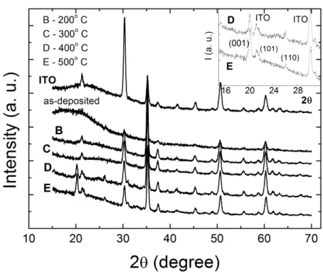
The x-ray diffractogram of as-deposited and heat-treated films and of the ITO film coated on the glass substrate are shown in Figure 1. Excluding the diffraction peaks belonging to the ITO x-ray pattern, no other peaks in the as-deposited or even in the annealed films at 200 and 300 ºC are observed. An amorphous ture is thus assigned to them. On the other hand, under annealing at 400 and 500 ºC ordered crystalline struc-tures were formed, since vanadium oxide peaks are observed in the diffractograms. The x-ray spectra reveal lines corresponding to the orthorhombic V2O5 polycrystalline lattice, assigned from the (001), (101) and
(110) crystalline planes (inset of Figure 1). However, the broad and low intensity diffraction peaks indicate that structural defects remain in the vanadium pentoxide structure, even after the annealing. A c parameter of 4.4 Å is calculated from the (001) peak, in good agreement with the literature values [14].
Figure 1: X-ray diffractograms for as-deposited and annealed vanadium oxide films. The inset shows the diffractograms for the D and E polycrystalline vanadium oxides. The diffractograms of the ITO layer x-ray is also shown.
as-deposited and annealed films at 200 and 300 ºC, as indicated by the x-ray spectra (Figure 1). Under heat treatment at 400 and 500 ºC, well-resolved Raman spectra are observed, with peaks at 104, 146, 198, 285, 305, 406, 483, 528, 702 and 996 cm-1, corresponding to the sequence obtained for V2O5 single crystal [15]
and polycrystalline vanadium oxide films [16].
The peak at 996 cm-1, superimposed on a plateau around 960 cm-1 is attributed to the vanadyl stretch-ing vibrational mode (V-OV). This plateau belongs to the underlying Si substrate [16] and its intensity
de-creases with the thickness of the vanadium oxide film, that act as a scattering source for the Si Raman radia-tion, as can be observed from figure 2. At 702 cm-1, a stretching vibration characterizes the (3V-OC) bonds.
The prominent peak at 146 cm-1 is due to the skeleton bending vibration, providing evidence that a layer-like structure was formed by the heat treatments at 400 and 500 ºC, and also suggesting that the polycrystalline V2O5 films grow with a preferred orientation about the c-axis perpendicular to the substrate plane, which is in
good agreement with the GAXRD measurements.
Figure 2: Raman spectra obtained for the as-deposited and thermally treated vanadium oxide films at various tempera-tures. The spectrum of the (100) silicon substrate is also presented.
Using RBS results was possible to estimate the elemental composition of the samples (data presented on Table 1). The as-deposited films have a low oxygen content (O/V = 1.96), the oxide films thermal treated at 200 (B film) and 300 ºC (C film) presented an excess of oxygen and the polycrystalline D and E films were both nonstoichiometric crystalline vanadium pentoxide, presenting O/V atomic ratio lower than 2,5.
As shown in Table 1 the as-deposited film was visually black, changing to transparent with a bluish grey color under annealing at 200 and 300 ºC, and to a yellow color, characteristic of crystalline vanadium pentoxide, when annealed at 400 and 500 ºC.
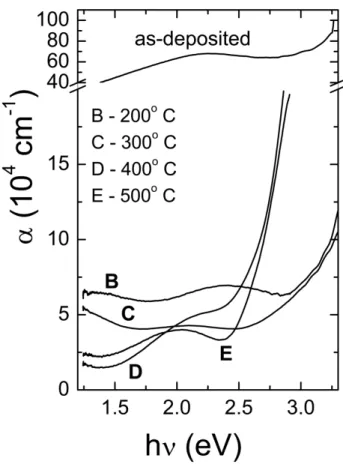
Figure 3 shows the optical absorption coefficient α for these films, calculated from equation (1), as function of incident photon energy hν. The following features can be clearly observed in the figure: (a) A high and featureless optical absorption coefficient, with α ranging from 105
to 106 cm-1 over the whole photon energy range, for the as-deposited films. (b) Under heat treatments at 200 and 300 ºC, both films develop optical absorption coefficients exhibiting similar trends: high and almost constant α values (~5.0 x10⁴
again present similar absorption features, a sharp and increasing optical absorption for hν > 2.5 eV, in which α grows very fast with photon energy and a lower absorption α in the 1.5 < hν < 2.5 eV energy region. The region where a rapid increase in α with hν is observed is characteristic of the fundamental absorption edge in semiconductor materials, resulting of electronic charge transference from the valence to the conduction band. The extended absorption region below about 2.5 eV accounts for transitions related to energy states within the energy band gap, as below explained.
Figure 3: Optical absorption coefficient α as a function of incident photon energy for as-deposited and for thermally-treated vanadium oxide films at various temperatures.
4. DISCUSSION
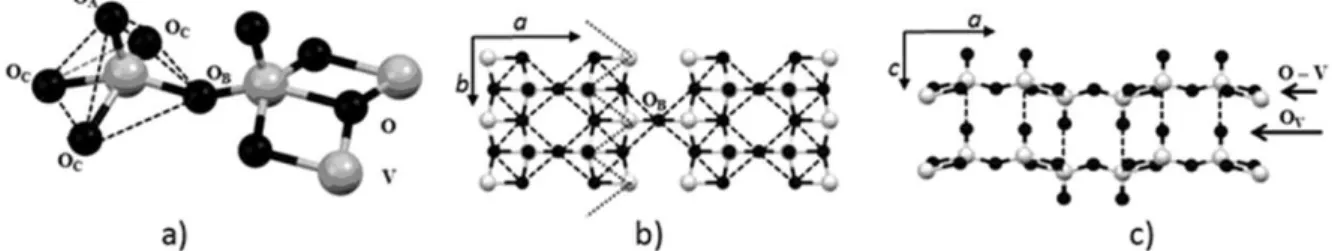
The crystalline structure of the vanadium pentoxide is well known: at room temperature has an orthorhombic structure [17] with each V atom surrounded by five O atoms which form the corners of a distorted square pyra-mid, as shown in Figure 4a. The oxygen atoms are designated according to their bonding to the vanadium atoms in the crystal lattice (OB, OC and OA) with the stronger and shortest bond occurring between V and OA, the
oxy-gen atom at the apex of the pyramid. In the b-crystallographic direction, oxyoxy-gen pyramids pointing alternatively up and down are joined to each other by sharing common edges, forming a zigzag chain, Figure 4b. These chains are linked to each other in the a-direction by OB bridging oxygen atoms, forming layers in the ab crystal
plane, Figure 4b. The layers are connected to each other by weak bonds between the V atoms of a layer with OA
atoms from the neighbor layer, in the c direction. The OA atoms of the neighbor layers are known as vanadyl
Figura 4: Vanadium coordination in a perfect V2O5 lattice (a); projection of the (010) planes of the V2O5 lattice, in which
the zigzag dotted lines indicate the oxygen pyramids pointing alternatively up (OA atom visible) and down (V atom visible)
in b direction (b); projection of the (001) planes (c).
The featureless x-ray diffraction and Raman spectra, resulting from a out of phase x-ray scattering and a lack of vibrational modes, both strongly dependent on the structure and geometry of the crystal, as well as the low O/V atomic ratio of the as-deposited vanadium oxide films, indicate a disordered crystal structure and a highly oxygen deficient oxides, for which a high density of V4+ and V3+ oxidation states is expected and, consequently, an high optical absorption [18], as was effectively measured, Figure 3. As-deposited films can be considered a nonstoichiometric amorphous VO2 oxide.
Thermal treatments at 200 and 300 ºC in Ar and rarified O2 atmosphere does not crystallizes the
amorphous as-deposited film that still retains long-range structural disorder, although some local order has occurred. A hypothesis for the high O/V atomic concentration rate for these two films (> 2.5) is the presence of molecular water or oxygen trapped into the disordered and porous as-deposited films during the film depo-sition or annealing, respectively. However, additional analyses must be performed to support this suppodepo-sition.
Annealing at 400 and 500 ºC (samples D and E, respectively) desorbs the trapped water and oxygen and structurally reorders the as-deposited amorphous films, as indicated by the x-ray and Raman spectra. The presence of peaks and specially the O vanadyl bond in the Raman spectra at 996 cm-1 is a probe of the struc-tural crystallinity for D and E films and its V2O5 coordination. However, the V/O atomic ratio lowers than
2.5 indicate nonstoichiometric vanadium pentoxide, with local oxygen vacancies. Vanadium valences of V5+, V4+ are expected for both films.
A relevant issue to be noted is the change in the film structure from amorphous to crystalline when the annealing temperature was changed from 300 to 400 ºC. Transitions in structure and composition have been reported for VOx films as function of atmosphere and annealing temperature [19].
The long and short range disorders occurring respectively, in the amorphous and polycrystalline semi-conductor vanadium oxide films, are reflected in the tail and edge shapes of the optical absorption curve, as shown in Figure 3. The absorption tails observed in the annealed films are generated by defects that introduce electronic states into the energy gap, allowing optical absorption for photons with energy lower than 2.5 eV.
The extended and almost constant optical absorption throughout a wide photon energy region and a featureless absorption edges indicate that a high density of energy states was created into the band gap of amorphous B and C films. These defects form an almost continuum of energy states between the valence and conduction bands, centered at 2.38 eV for the film annealed at 200 ºC. Heat treatment at 300 ºC decreases α some more in the tail region, and a more uniform band structure begins to be defined at the absorption edge.
At higher annealing temperatures (400 and 500 ºC) the optical absorption in the tail region present a broad peak at 2.0 eV for the E film, indicating that defect states within the energy band gap are centered in this energy. The inflexion around 2.0 eV in the curve of the D film indicates that two or more center of defects states are formed into the band gap of this film. A well-defined band structure, however, is now ob-tained for these polycrystalline vanadium oxide films, as revealed by a sharp absorption edge starting at 2.5 eV.
Optical absorption in low energy region is associated with defect states within the band gap generated by charged V+4 and V3+ ions [18, 20]. A high concentration of V+4 and V3+ ions is expected in the amorphous samples B and C, from the general disorder of its bonding. Increasing the annealing temperatures promotes vanadium oxidation and, as consequence, decreasing the relative concentration of V+4 and V3+ ions and the optical absorptions in the tail region, as observed from Figure 3.
oxi-dation which occurred during annealing at 400 and 500 ºC establishes the V-OV bonds, as observed by the
presence of the corresponding peaks in the Raman spectra, Figure 2. But part of the O vanadyl vacancies re-main in the oxide structure, since a nonstoichiometric O/V < 2.5 ratio was observed from the RBS measure-ments
The differences in shape and photon energy range of the absorption edge observed between the amor-phous (B and C) and polycrystalline (D and E) semiconductor films, Figure 3, can be attributed to the change in the V-O coordination in these two morphologies [18]. In amorphous films B and C, the V atoms are disor-derly bonded to O atoms, while for samples D and E, the octahedral V-O coordination is predominant. This explains the great difference in the slope of the absorption edge: whereas a barely defined edge is observed for the amorphous films, clearly identified edges were obtained for the polycrystalline samples.
In semiconductors, the absorption edge has a polynomial dependence on the photon energy, hν, which varies with the nature of electronic band-to-band transition. In films with sufficient disorder, as in amorphous and nonstoichiometric polycrystalline films, an indirect allowed transition between the valence and conduc-tion bands is supposed to exist, for which
2
(
h
)
B h
(
E
o)
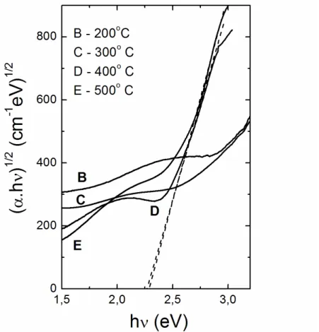
(2)Where B is a constant, E0 is the optical band gap and hν > E0 [21]. Theoretical calculation of the band structure and the density of states for V2O5 also indicate indirect transitions across the main gap [22].
Figure 5 shows (αhν)1/2 as function of hν for the annealed samples at 400 and 500 ºC. An optical band gap around 2.25 eV was obtained for both D and E polycrystalline samples, in good agreement with those reported for polycrystalline sputtered vanadium pentoxide films [18, 23].
Figure 5: (αhν)1/2 as a function of incident photon energy for vanadium oxide films annealed at the temperatures indicat-ed in the top left corner. The dashindicat-ed line is a fit of the linear part of the optical absorption indicat-edge for D and E films.
5. CONCLUSION
changes the composition, the structure and the optical absorption of the as-deposited film. The films treated at 200 and 300 ºC are still amorphous, but optically transparent. A high optical absorption tail and a broad absorption edge indicate that oxygen vacancies and vanadium in V3+ and V4+ oxidation states are present in these structurally disordered oxides. When annealed at 400 and 500 ºC a nonstoichiometric polycrystalline vanadium pentoxide is formed in an orthorhombic structure with a well-defined absorption edge for which an optical band gap of 2,25 eV was measured and V4+ and V5+ oxidation states are supposed to be formed. The ex-situ annealing method under controlled argon and oxygen atmospheres showed to be a simple an efficient method to modulate the structure and optical properties of as-deposited amorphous and opaque vanadium oxide films, that can be applied to others metal oxides. The film properties modulate by this method are simi-lar to those obtained by controlling the deposition parameters in traditional vacuum deposition techniques. Both, the HFMOD technique and the ex-situ annealing method can be simple and low cost alternatives for metal oxide thin film processing.
6. ACKNOWLEDGMENTS
Funding for this work was provided by Sercomtel Celular S.A. and the Brazilian agencies FAPESP and CNPq. P.R.C. Silva thanks the Brazilian agency CAPES for his scholarship. The authors are grateful to Dr. Lisandro P. Cardoso for use of the X-ray facilities and to Dr. F. Ikawa for the Raman spectra acquisition.
7. BIBLIOGRAPHY
[1] GRANQVIST, C.G., Handbook of Inorganic Electrochromic Materials, 3ª ed., Amsterdam, Elsevier, 1995.
[2] CHIU, T.-L., CHUANG, Y.-T., “Spectral observations of hole injection with transition metal oxides for an efficient organic light-emitting diode”, Journal of Physics D: Applied Physics, v. 48, n. 075101, pp. 1-6, Jan. 2015.
[3] LUO, Y.Y., ZHU, L.Q., ZHANG, Y.X., et al., “Optimization of microstructure and optical properties of VO2 thin film prepared by reactive sputtering”, Journal of Applied Physics, v. 113, n. 183520, pp. 1-7, May
2013.
[4] XU, G., JIN, P., TAZAWA, M., YOSHIMIRA, K., “Optimization of antireflection coating for VO2-based
energy efficient window”, Solar Energy Materials and Solar Cells, v. 83, pp. 29–37, Jun. 2004.
[5] LIN, Y.-S., TSAI, C.-W., CHEN, P.-W., “Electrochromic properties of V2O5-z thin films sputtered onto
flexible PET/ITO substrates”, Solid State Ionics, v. 179, pp. 290–297, Apr. 2008.
[6] ÖKSÜZOĞLU, R.M., BILGIÇ, P., YILDIRIM, M., et al., “Influence of post-annealing on electrical, structural and optical properties of vanadium oxide thin films”, Optics & Laser Technology, v. 48, pp. 102– 109, Jun. 2013.
[7] ROUXINOL, F.P., TRASFERETTI, B.C., LANDERS R., et al., “Hot-Filament Metal Oxide Deposition (HFMOD): A Novel Method for Depositing Thin Films of Metallic Oxides”. Journal of the Brazilian Chemi-cal Society, v. 15, n. 2, pp. 324–326, Fev. 2004.
[8] DÍAZ-REYES, J., CASTILLO-OJEDA, R., GALVÁN-ARELLANO, M., et al., “Characterization of WO3 Thin Films Grown on Silicon by HFMOD”, Advances in Condensed Matter Physics, v. 2013, n. 591787,
pp. 1-9, Jul. 2013.
[9] DÍAZ-REYES, J., DELGADO-MACUIL, R.J., DORANTES-GARCÍA, V., et al, “Physical properties characterization of WO3 films grown by hot-filament metal oxide deposition”, Materials Science and
Engi-neering: B, v. 174, n. 1–3, pp. 182–186, Oct. 2010.
[10] DURRANT, S.F., TRASFERETTI, B.C., SCARMINIO, J., et al., “Developments in hot-filament metal oxide deposition (HFMOD)”, Thin Solid Films, v. 516, p. 789-793, Jul. 2008.
[11] BAMROONGWONGDEE, C., BOWKER, M., CARLEY, A.F., et al., “Fabrication of complex model oxide catalysts: Mo oxide supported on Fe3O4(111)”, Faraday Discuss, v. 162, pp. 201-212, 2013.
[12] MORAES, M.A.B., TRASFERETTI, C., ROUXINOL, F.P., et al., “Molybdenum Oxide Thin Films obtained by the hot-filament metal oxide deposition technique”, Chemistry of Materials, v. 16, pp. 513-520, 2004.
[13] DOOLITTLE, L.R., “Algorithms for the rapid simulation of Rutherford backscattering spectra”, Nuclear Instruments and Methods in Physics Research Section B: Beam Interactions with Materials and Atoms, v. 9, n. 3, pp. 344-351, Jun. 1985.
V2O5 thin films”, Thin Solid Films, v. 516, pp. 912-918, 2008.
[15] ABELLO, L., HUSSON, E., REPELIN, Y., et al., “Vibrational spectra and valence force field of crys-talline V2O5”, Spectrochimica Acta Part A: Molecular Spectroscopy, v. 39, n. 7, pp. 641-651, 1983.
[16] JULIEN, C., HARO-PONIATOWSKI, E., CAMACHO-LÓPEZ, M.A., et al., “Growth of V2O5 thin
films by pulsed laser deposition and their applications in lithium microbatteries”, Materials Science and En-gineering: B, v. 65, n. 3, pp. 170–176, Nov. 1999.
[17] ENJALBERT, R., GALY, J., “A refinement of the structure of V2O5”, Acta Crystallographica Section C,
v. 42, pp. 1467-1469, 1986.
[18] AITA, C.R., LIU, Y.L., KAO, M.L., et al., “Optical behavior of sputter-deposited vanadium pentoxide”. Journal of Applied Physics, v. 60, n. 2, pp. 749-753, 1986.
[19] GOLTVYANSKYI, Y., KHATSEVYCH, I., KUCHUK, A., et al., “Structural transformation and func-tional properties of vanadium oxide films after low-temperature annealing”, Thin Solid Films, v. 564, pp. 179-185, 2014.
[20] AITA, C.R., KAO, M.L., “Low-temperature oxidation of nonstoichiometric sputter deposited vanadium pentoxide”, Journal of Vacuum Science & Technology A, v. 5, n. 4, pp. 2714, 1987.
[21] KHAN, G.A., HOGARTH, C.A., “Optical absorption spectra of evaporated V2O5 and co-evaporated
V2O5/B2O3 thin films”, Journal of Materials Science, v. 26, n. 2, pp. 412-416, Jan. 1991.
[22] BULLET, D.W., “The energy band structure of V2O5: a simpler theoretical approach”, Journal of
Phys-ics C: Solid State PhysPhys-ics, v. 13, n. 23, pp. L595-L599, 1980.