October
2019Miguel Alexandre Branco Tibério
[Nome completo do autor]
[Nome completo do autor]
[Nome completo do autor]
[Nome completo do autor]
[Nome completo do autor]
[Nome completo do autor]
[Nome completo do autor]
Bachelor in Science of Micro and Nanotechnologies Engineering
[Habilitações Académicas] [Habilitações Académicas] [Habilitações Académicas] [Habilitações Académicas] [Habilitações Académicas] [Habilitações Académicas] [Habilitações Académicas]
Study of
localized
transport phenomena of Cu
2O
Dissertation submitted in partial fulfillment of the requirements for the degree of
Master of Science in
Micro and Nanotechnologies Engineering
Dissertação para obtenção do Grau de Mestre em
[Engenharia Informática]
Supervisor: Dr. Jonas Deuermeier, Postdoctoral Researcher, Faculdade de
Ciências e Tecnologia, Universidade Nova de Lisboa
Co-supervisor: Dr. Suman Nandy, Postdoctoral Researcher, Faculdade de
Ciências e Tecnologia, Universidade Nova de Lisboa
Study of localized transport phenomena of Cu2O
Copyright © Miguel Alexandre Branco Tibério, Faculdade de Ciências e Tecnologia, Universidade Nova de Lisboa.
Faculdade de Ciências e Tecnologia and Universidade Nova de Lisboa have the right, perpetual and without geographical boundaries, to file and publish this dissertation through printed copies reproduced on paper or on digital form, or by any other means known or that may be invented, and to disseminate through scientific repositories and admit its copying and distribution for non-commercial, educational or research purposes, as long as credit is given to the author and editor.
Acknowledgements
First of all, I would like to thank Dr. Jonas Deuermeier for guiding me through all this process. You’ve always been very helpful and kind, and I appreciate all the time you spent with me. You really contributed for making this experience better. I need to thank Dr. Suman Nandy as well for his help. I won’t forget that time at the lab where I learned more about the sacrifices you made to be where you are now. Tomás Calmeiro also deserves a huge acknowledgement for all the effort he put on the AFM measurements. You definitely made this work a lot richer and those silent times on the lab funnier. I would also like to thank Prof. Dr. Daniela Nunes for making the SEM meas-urements, and to Alexandra Gonçalves and Sónia Pereira for the help they provided me in the lab.
Agradeço ao André, o meu padrinho, por me ter acompanhado durante o meu percurso académico. Obrigado por todas as conversas que nos tornaram amigos. Obrigado também por teres feito os dias passarem mais rápido e por me teres evitado algumas viagens à faculdade. À Filipa e ao Miguel, obrigado por terem tornado o meu percurso académico sem dúvida mais feliz.
Aos meus amigos de sempre e para sempre: Ana, Castelo, Filipa, João, Mel e Tiago. Obrigado por me darem tantas alegrias, gargalhadas, conforto. Obrigado pelas viagens e pelas histórias. Obrigado por estarem aqui, especialmente quando é mais difícil. Ao Dan, um agradecimento duplo por ser um apoio dentro e fora da faculdade. Ao Rodrigo, o amigo que podia ser irmão. Obrigado por me ensinares que, no jogo que é a vida, a amizade vence a distância.
Ao Nuno, que me deu o que eu mais precisava nesta fase: repreensões e amor. Um não se dissocia do outro, não é? Obrigado por tentares dar-me algum ânimo, mesmo quando parecia não ter efeito. Obrigado por me ouvires quando só me apetecia desistir. E obrigado por estares comigo, incondicionalmente.
Um obrigado especial aos que mais contribuíram para o meu crescimento e que me deram tanto, especialmente durante a infância: tia Olga, avó Bárbara, avô António, avó Amélia. Aos meus pais, um obrigado pelos avisos sucessivos sobre o prazo de entrega da tese. Acho que já o decorei. Agora mais a sério, obrigado pela preocupação. E obrigado pelo investimento que fizeram em mim ao longo destes anos. Apesar de às vezes não parecer, tenho noção de que não há investimento mais bonito e altruísta do que aquele que se faz num filho. Espero, um dia, vir a investir assim em alguém.
Abstract
Cu2O is a p-type semiconductor with a wide range of applications in optoelectronics, namely solar cells. Performance limitations have been previously ascribed to an inhomogeneous local conductivity: notably highly conductive grain boundaries compared to the grains. In this work, pol-ycrystalline Cu2O thin-films fabricated by reactive sputter deposition were studied. In addition, Cu2O particles with cubic and octahedral shapes were produced from solution. The facets of cubic particles have a (100) orientation, whereas octahedral particles have facets with (111) orientation. Electrical modes of atomic force microscopy were used to study the localized transport mecha-nisms of the differently prepared Cu2O samples. Remarkably, the thin-film Cu2O samples of this work all showed more conductive grains compared to the grain boundaries. The results were an-alyzed in conjunction with structural, chemical, optical and morphological information.
Keywords: local conductivity; grain boundaries; facets; conductive atomic force microscopy;
Resumo
O Cu2O é um semicondutor tipo-p com uma vasta gama de aplicações, nomeadamente células solares. Algumas limitações de desempenho têm sido atribuídas a uma condutividade local não-homogénea: fronteiras de grão altamente condutoras comparativamente aos grãos. Neste trabalho, foram estudados filmes-finos de Cu2O policristalino fabricados por sputtering reativo. Para além disso, foram produzidas partículas de Cu2O com formas cúbicas e octaédricas através de solução. As faces das partículas cúbicas têm uma orientação (100), enquanto as partículas octaédricas têm faces com orientação (111). De forma a estudar os mecanismos de transporte localizados das diferentes amostras de Cu2O preparadas, foram utilizados modos elétricos de microscopia de força atómica. Curiosamente, todos os filmes-finos de Cu2O produzidos no decorrer deste trabalho mostraram ter grãos mais condutores comparativamente às fronteiras de grão. Os resultados foram analisados em conjunto com informação estrutural, química, ótica e morfológica.
Palavras-Chave: condutividade local; fronteiras de grão; faces; microscopia de força
Contents
1. INTRODUCTION 1
2. EXPERIMENTAL PROCEDURE 3
2.1. CU2OTHIN-FILM DEPOSITION 3
2.2. CU2OPARTICLE SYNTHESIS 4
2.3. CHARACTERIZATION TECHNIQUES 5
3. RESULTS AND DISCUSSION 9
3.1. THIN-FILMS 9
3.1.1. TRANSMITTANCE SPECTROSCOPY 9
3.1.2. X-RAY DIFFRACTION 11
3.1.3. SCANNING ELECTRON MICROSCOPY 14
3.1.4. X-RAY PHOTOELECTRON SPECTROSCOPY 15
3.1.5. ATOMIC FORCE MICROSCOPY AND CONDUCTIVITY MEASUREMENTS 16
3.2. PARTICLES 23
3.2.1. SCANNING ELECTRON MICROSCOPY 23
3.2.2. X-RAY DIFFRACTION 25
3.2.3. ENERGY DISPERSIVE X-RAY SPECTROSCOPY 25
3.2.4. ATOMIC FORCE MICROSCOPY 26
4. CONCLUSIONS AND FUTURE PERSPECTIVES 29
REFERENCES 31 ANNEXES 33 ANNEX A 33 ANNEX B 34 ANNEX C 34 ANNEX D 34
List of Figures
Figure 2.1 – (a) LP, (b) HP and (c) LP-SB sets of Cu2O thin-films. These thin-films were deposited on ITO-coated glass and they are organized, from left to right, by an increasing O2 flow rate. ... 4 Figure 2.2 – (a) Cu2O thin-films deposited on three different substrates (top-right: corning glass;
top-left: ITO-coated glass; bottom: silicon); (b) Cu2O particles prepared by two different methods (left: powder on carbon tape; drop-casted films). ... 6 Figure 3.1 – Tauc plots of (a) LP, (b) HP and (c) LP-SB sets of Cu2O thin-films, consisting of four
LP samples, five HP samples and three LP-SB samples deposited using different O2 flow rates. ... 10 Figure 3.2 – XRD results of the LP set of Cu2O thin-films, consisting of four samples deposited
using different O2 flow rates. The main peaks of Cu2O are represented by the dashed lines. ... 11 Figure 3.3 – XRD database references of copper oxides (Cu2O, CuO and Cu4O3) and metallic
Cu... 12 Figure 3.4 – XRD results of the most stoichiometric Cu2O thin-films from each set (LP-SB, LP
and HP), including HP-heated film. The main peaks of Cu2O are represented by the dashed lines. ... 13 Figure 3.5 – XRD results of two Cu2O thin-films from the HP set, deposited using 0.7 sccm and
0.8 sccm O2 flow rates. The main peaks of Cu2O are represented by the dashed lines. ... 14 Figure 3.6 – SEM cross-sectional image of the most stoichiometric LP Cu2O thin-film deposited
on a silicon substrate. ... 15 Figure 3.7 – XPS data from (a) Cu 2p and (b) O 1s emissions relative to the LP set of films,
consisting of four samples deposited using different O2 flow rates. ... 15 Figure 3.8 – Mask applied by Gwyddion software. The IG was measured outside the mask. ... 16 Figure 3.9 – Topographic images and respective current maps of every Cu2O thin-film from the
LP set, consisting of four samples deposited using different O2 flow rates: (a) 1.1 sccm, (b) 1.2 sccm, (c) 1.3 sccm and (d) 1.4 sccm. ... 17 Figure 3.10 – Topographic images and respective current maps of the most stoichiometric Cu2O
thin-films from each set: (a) LP-SB, (b) LP and (c) HP, including (d) HP-heated film. ... 18 Figure 3.11 – Topographic images and respective current maps of Cu2O thin-films deposited
xvi
samples deposited during different times: (a) 7.5 minutes, (b) 15 minutes, (c) 30 minutes and (d) 60 minutes. ... 20 Figure 3.12 – Topographic images and respective current maps of Cu2O thin-films from the HP
set with different preferential orientations, consisting of two samples deposited using
different O2 flow rates: (a) 0.7 sccm and (b) 0.8 sccm. ... 21 Figure 3.13 – (a) Topographic image and (b) respective current map of the LP film deposited
using a 1.1 sccm O2 flow rate. The top half of either image was obtained by using a -2 V voltage and the bottom half using a +2 V voltage. ... 22 Figure 3.14 – (a) Topographic image and (b) respective current map of the most stoichiometric
Cu2O thin-film from the HP set obtained by Cypher S. ... 23 Figure 3.15 – SEM images of (a) cubic and (b) octahedral particles obtained in the 1st synthesis.
... 24 Figure 3.16 – SEM images of (a) cubic and (b) octahedral particles obtained in the 2nd synthesis.
... 24 Figure 3.17 – XRD results from cubic and octahedral particles obtained in the 1st synthesis. The
main peaks of Cu2O are represented by the dashed lines... 25 Figure 3.18 – (a) Topographic image and (b) respective current map of unoptimized octahedral
particles obtained by a Cypher S system. ... 26 Figure 3.19 – (a) Topographic image and (b) respective current map of octahedral particles from
the 1st synthesis obtained by a MFP-3D-SA system. ... 27 Figure 3.20 – Topographic images and respective resistivity maps of (a) cubic and (b) octahedral
List of Tables
Table 2.1 – Parameters used in the sputter deposition of the three sets of Cu2O thin-films: LP, HP and LP-SB. ... 3 Table 2.2 – Summary of the characterization techniques used to analyze the Cu2O structures
produced (films and particles), organized by the type of properties provided. ... 5 Table 3.1 – Most stoichiometric Cu2O thin-films from each set (LP, HP and LP-SB) and
respective bandgaps... 10 Table 3.2 – IG, σOOP-G and σIP of every Cu2O thin-film from the LP set, consisting of four samples
deposited using different O2 flow rates. ... 18 Table 3.3 – IG, σOOP-G and σIP of the most stoichiometric Cu2O thin-films from each set, including
HP-heated film. ... 19 Table 3.4 – IG, σOOP-G and σIP of Cu2O thin-films deposited under the conditions of the most
stoichiometric film from the LP set, consisting of four samples deposited during different times. ... 20 Table 3.5 – IG, σOOP-G and σIP of Cu2O thin-films from the HP set with different preferential
orientations, consisting of two samples deposited using different O2 flow rates. ... 21 Table 3.6 – Oxygen content of cubic and octahedral particles from both syntheses, obtained by
List of Abbreviations
AFM atomic force microscopy α absorption coefficient
Atip area of the bigger AFM tip cross-section CAFM conductive atomic force microscopy
d distance between consecutive crystallographic planes EDS energy-dispersive X-ray spectroscopy
HP higher pressure
ICDD International Centre for Diffraction Data IG average grain current
IPA isopropyl alcohol ITO indium tin oxide
KPFM Kelvin probe force microscopy
λ wavelength
LP lower pressure
LP-SB lower pressure with substrate bias PDF Powder Diffraction File
PVP polyvinylpyrrolidone
R reflectance
RF radio-frequency
SEM scanning electron microscopy σIP in-plane conductivity of a film
σOOP-G out-of-plane conductivity of the grains
T transmittance
tfilm film thickness
θ glancing angle
VCAFM voltage used during CAFM measurements XPS X-ray photoelectron spectroscopy
1
1. Introduction
Nowadays, characteristics like flexibility and transparency are becoming almost mandatory relatively to electronic devices. While n-type transparent oxide semiconductors are being devel-oped with great results, p-type ones are facing several difficulties related to performance. Metal oxides like NiO and SnO are being studied with the purpose to fill that gap, although cuprous oxide is one of the big candidates. In the form of a thin-film, it has great potential due to its 2.17 eV bandgap (which makes it semi-transparent) and to the possibility of being prepared at low temper-ature (allowing its deposition on flexible substrates). Besides that, it is abundant in ntemper-ature, non-toxic and it has a low production cost. [1]
Despite all the advantages of using Cu2O, its implementation on p-type thin-film transistors (TFTs), complementary metal-oxide-semiconductor (CMOS) devices and solar cells is limited due to some performance drawbacks. Unlike Cu2O in bulk form, Cu2O TFTs are demonstrating a high conductivity in the off-state and a low field-effect mobility, which makes the devices unfunc-tional. [2] It is known that the polycrystalline structure of the Cu2O thin-films is in the center of the problem, which is aggravated when Cu2O is deposited at low temperatures since the grains be-come smaller. [3]
It is reported that Cu2O grain boundaries are mainly formed by CuO, with a higher conduc-tivity, which masks the current rectification properties from the Cu2O grains. [2], [4] Besides that, grain boundaries act as shunt paths, affecting carrier mobility. [5]
Cu2O can be deposited by different techniques, namely, sputtering, pulsed laser deposition, molecular beam epitaxy, chemical vapor deposition and electrochemical deposition. [3] In this work, Cu2O thin-films were produced by reactive sputter deposition. The main goal was to repro-duce the behavior described above in which the grain boundaries were more conductive than the grains. To observe that, atomic force microscopy (AFM) and one of its electrical modes, conductive atomic force microscopy (CAFM), were intensely used, as in other works. [5], [6] After altering the deposition parameters several times and even performing post-deposition heating treatments on the films, the opposite situation was constantly observed: the grains were more conductive than the grain boundaries. This behavior was not yet reported.
Previously, some differences in electrical behavior of the films were ascribed to metallic pre-cipitates inside Cu2O. [7] However, the facets of grain interfaces present in the films can also have influence. Several facet-dependent behaviors on Cu2O have been studied. For example: (111)-textured films have higher carrier mobility [8]; photocatalytic activity is described as higher in the
(111) direction compared to (100) oriented facets [9]; CAFM shows that the conductivity of an octahedral particle is different along one of its (111) facets [10]; electrical conductivity is reported to be higher between (111) facets of an octahedral particle than between (100) facets of a cubic particle. [11]
Although it is not simple to control the facet orientation of grains in a film, particles allow that kind of control. [12], [13] In this work, Cu2O particles were produced from solution in two different shapes: cubic particles with (100) facets and octahedral particles with (111) facets.
3
2. Experimental Procedure
2.1.
Cu
2O Thin-film Deposition
The deposition of the Cu2O thin-films was made by reactive radio-frequency (RF) magnetron sputtering and the system used was an ATC-Orion 8 UHV from AJA International. It was used a 2 inch (5.08 cm diameter) copper target with a 99.99% purity from Plasmaterials.
To allow the thin-film characterization by different techniques, the films were deposited on three different substrates: corning glass, indium tin oxide (ITO)-coated corning glass and silicon. These substrates were previously cleaned in an ultrasound bath with acetone, followed by isopro-pyl alcohol (IPA), for 10 minutes each. Then, the films were washed with deionized water and dried with compressed nitrogen.
The first depositions were not resulting in uniform films, so an adjusting of the magnetron tilting was required (0.95’24 was the optimized value). After that, several parameters were kept constant, while others were altered to understand their influence on the films. All these parameters are presented in Table 2.1. The films were deposited under three different main conditions: lower pressure (LP), higher pressure (HP) and lower pressure with substrate bias (LP-SB). LP set of films was the first to be deposited. Depositing under HP and LP-SB conditions would theoretically result, respectively, in less dense and denser films. That could be interesting to understand if the film density would influence other properties of the films, namely, structural and electrical.
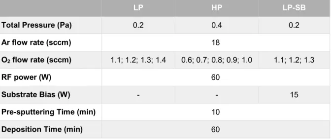
Table 2.1 – Parameters used in the sputter deposition of the three sets of Cu2O thin-films: LP, HP and LP-SB.
LP HP LP-SB
Total Pressure (Pa) 0.2 0.4 0.2
Ar flow rate (sccm) 18
O2 flow rate (sccm) 1.1; 1.2; 1.3; 1.4 0.6; 0.7; 0.8; 0.9; 1.0 1.1; 1.2; 1.3
RF power (W) 60
Substrate Bias (W) - - 15
Pre-sputtering Time (min) 10
All the depositions occurred at room temperature and with the maximum level of substrate rotation set on. Parameters like RF power and deposition time were also kept constant among the three sets of films. The 10 minutes of pre-sputtering are important to make sure that, when a deposition starts, the conditions of the target surface have stabilized. The goal was to deposit Cu2O thin-films, so an ideal Cu/O ratio of 2:1 had to be achieved. Knowing that a Cu2O film has a yel-lowish color, the Ar flow rate was kept constant while the O2 flow rate was adjusted by observing the color of the films obtained. The three sets of films are displayed in Figure 2.1.
To understand the possible influence of film thickness on other film properties, thinner films were deposited in LP conditions by halving the deposition time successively (30 min; 15 min; 7.5 min). Also, to verify the influence of oxidizing the films by temperature, the most stoichiometric film from the HP set was later heated for 24 hours at 100 °C in a post-deposition treatment.
2.2.
Cu
2O Particle Synthesis
The synthesis of the Cu2O particles was based on a published article. [13] To investigate the influence of the particle shape on other properties, cubic and octahedral particles have been made by the same solution-based method. The particles have been made simultaneously, in dif-ferent containers. The synthesis of either shape of particles only differs in a single step, which will be highlighted. The quantities present in the following procedure refer to a single container where
Figure 2.1 – (a) LP, (b) HP and (c) LP-SB sets of Cu2O thin-films. These thin-films were deposited on ITO-coated glass and they are organized, from left to right, by an increasing O2 flow rate.
5
will occur a synthesis of a specific particle shape. The quantities are the same for the other con-tainer.
First of all, 100 mL of a CuCl2 · 2H2O aqueous solution (0.01 M) were prepared. To obtain octahedral particles, 3.334 g of polyvinylpyrrolidone (PVP), with a weight average molecular weight of 10 000 g/mol, was added to the previous solution. No PVP was added to the synthesis of the cubic particles. Then, 10 mL of a NaOH aqueous solution (2 M) was added dropwise, followed by 30 minutes of waiting. After that, 10 mL of an ascorbic acid aqueous solution (0.6 M) was added, also dropwise, followed by 3 hours of waiting. The whole process occurred under constant stirring and in a 55 °C water bath. The solution was then centrifuged (6000 rpm, 15 minutes) and decanted. The resulting precipitate was washed 3 times with distilled water and twice with ethanol (6000 rpm, 10 minutes each). In the end, the precipitate was dried at room temperature, resulting in a powder.
2.3.
Characterization Techniques
Several characterization techniques were used to analyze the Cu2O structures produced: profilometry, transmittance spectroscopy, X-ray diffraction (XRD), scanning electron microscopy (SEM), energy-dispersive X-ray spectroscopy (EDS), X-ray photoelectron spectroscopy (XPS), re-sistivity measurements and atomic force microscopy (AFM), in conjunction with conductive atomic force microscopy (CAFM), one of its electrical modes. In Table 2.2, it is possible to observe which techniques were used to characterize either the films or the particles and the type of information they provide.
Table 2.2 – Summary of the characterization techniques used to analyze the Cu2O structures produced (films and particles), organized by the type of properties provided.
Properties Films Particles
Morphological SEM (cross-section) Profilometry AFM
SEM AFM
Structural XRD XRD
Optical Transmittance Spectroscopy -
Chemical XPS XPS
EDS
Electrical Conductivity measurements CAFM CAFM
As mentioned before, the films were deposited on various substrates so they could be ana-lyzed by the different techniques. The particles were also prepared in different ways to facilitate the characterization process. Figure 2.2 displays the films deposited on different substrates and
the particles prepared by different methods. Below, the details on each technique are explained, namely, the sample preparation involved, the equipment and the parameters used.
Profilometry (XP-200 from Ambios) was used to measure the thickness of the films. The measurements were made on the films deposited on glass since it is a relatively flat substrate.
Transmittance spectroscopy (Lambda 950 from PerkinElmer) allowed obtaining optical in-formation of the films, namely the optical bandgap. The films deposited on glass were analyzed since glass is transparent to a wide range of wavelengths.
XRD (X'Pert PRO MRD from PANalytical) provided structural information of both Cu2O struc-tures. Regarding the films, an amorphous substrate was needed, so the films deposited on glass were analyzed. The particle structure was verified by placing the powder directly into a suitable holder.
SEM (Auriga CrossBeam from ZEISS) allowed obtaining morphological information of both Cu2O structures. To prevent any charge accumulation, SEM is a technique that requires substrates with conductive properties. For that reason, the films deposited on silicon were used. To obtain cross-sectional images, the films were manually broken prior to the measurement. The particles also required a specific preparation. The powder was transferred to a carbon tape which was pre-viously fixed on an ITO-coated glass. The powder excess was then blown with compressed nitro-gen. In addition, chemical information of the particles was obtained by EDS (X 150 from
Nano-Analysis) while in the SEM chamber.
XPS (AXIS Supra from Kratos Analytical with a monochromated Al Kα X-ray source) was used to obtain chemical information from the surface of both Cu2O structures. To prevent any charge accumulation, similarly to SEM, films deposited on ITO-coated glass were used. The films were analyzed with a 225 W X-ray power, no aperture and a 5 eV pass energy. The particle prep-aration used was the same as in SEM. The particles were analyzed with a 300 W X-ray power, a 110 µm aperture and a 20 eV pass energy.
Figure 2.2 – (a) Cu2O thin-films deposited on three different substrates (top-right: corning glass; top-left: ITO-coated glass; bottom: silicon); (b) Cu2O particles prepared by two different methods (left: powder on carbon tape; drop-casted films).
7
The conductivity of the films was also measured by the van der Pauw method with a Hall Effect measurement system (HL5500 from Nanometrics). Before that, Au contacts (with a thin Ni layer as adhesion promoter) were deposited by electron beam evaporation (home-made appa-ratus). For this technique, the films deposited on glass were used.
AFM was used to collect topographical information from both Cu2O structures, whereas CAFM, one of AFM electrical modes, allowed obtaining their local conductivity properties. CAFM requires a substrate with conductive properties, so the films deposited on ITO-coated glass were used. Most of AFM/CAFM measurements on the films were performed by an MFP-3D-SA system from Asylum Research. As AFM and CAFM are both contact mode techniques, a Nanoworld
CONTPt probe (f0 = 13 kHz, k = 0.2 N/m) was used. All CAFM images were obtained by applying -2 V to the ITO present on the substrate of the films. One of the measurements was executed by a Cypher S system, also from Asylum Research.
Regarding the particles, the same preparation used in SEM and XPS analysis was tested in the AFM/CAFM measurements. Nonetheless, and to prevent the powder to be dragged from the tape, a film was made from the particles by drop-casting. First, the powder was dispersed into distilled water with an ultrasonic probe. To improve the adhesion of the dispersion to the ITO-coated glass, circular spots were activated with a UV-ozone system. The dispersion was then dropped using a micropipette. The water evaporated at room temperature, forming circular films with the dried powder. By chronological order, the particles were analyzed using Cypher S and
MFP-3D-SA systems from Asylum Research (drop-casted films) and using a Nano-Observer
sys-tem from Concept Scientific Instruments (powder on carbon tape).
9
3. Results and Discussion
3.1.
Thin-films
3.1.1. Transmittance Spectroscopy
After depositing thin-films with different Cu/O ratios, transmittance spectroscopy was used. Since copper-containing materials can be distinguish by their absorption behaviors, this was the first technique to be used to verify which conditions lead to the formation of Cu2O. [14] In the case of copper oxides (Cu2O, CuO, Cu3O4), Cu2O is the one with the highest bandgap, i.e., it starts absorbing at higher energies. In addition, contributions of metallic copper in Cu2O would lead to an increased absorption at lower energies, compared to pure Cu2O. [15]
To verify these differences, the absorption coefficient (α) was calculated from the transmit-tance data by Lambert-Beer law (1). The reflectransmit-tance (R) was neglected since it only has a signifi-cant contribution on sub-bandgap absorption features. Only transmittance (T) was considered.
α =ln ( T 1 − R) tfilm
(1)
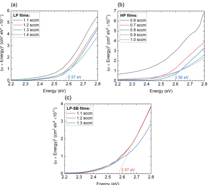
In the formula, tfilm represents the thickness of the films which was previously measured by the profilometer. The average thickness of the films was 265 nm, later confirmed by SEM meas-urements. Finally, a Tauc plot was made for each set of Cu2O thin-films (LP, HP and LP-SB). The most stoichiometric Cu2O thin-film from each set corresponds to the sample that starts absorbing at higher energies. The bandgap of the most stoichiometric films was then determined by extrap-olating the linear zone of the plot, as represented in Figure 3.1.
With the results observed in the three plots, Table 3.1 summarizes the oxygen flow rate and the bandgaps of the most stoichiometric Cu2O thin-films.
Table 3.1 – Most stoichiometric Cu2O thin-films from each set (LP, HP and LP-SB) and respective bandgaps.
LP HP LP-SB
O2 flow rate (sccm) 1.3 0.8 1.2
Bandgap (eV) 2.57 2.56 2.57
The results obtained by transmittance spectroscopy are in line with the evaluation of the color of the films. In addition, all three samples corresponding to the most stoichiometric Cu2O thin-films show a consistent bandgap value between 2.56 and 2.57 eV. Although the fundamental bandgap of Cu2O is 2.17 eV, the estimation using transmittance data generally leads to higher values, since the absorption at lower energy is not resolvable by this technique. [15]
Figure 3.1 – Tauc plots of (a) LP, (b) HP and (c) LP-SB sets of Cu2O thin-films, consisting of four LP samples, five HP samples and three LP-SB samples deposited using different O2 flow rates.
11
To complete the analysis, a shift to the left between the HP films deposited using 0.8 sccm and 0.7 sccm O2 flow rates can be observed. The same happens between the LP films deposited using 1.3 sccm and 1.2 sccm O2 flow rates, although it is not so pronounced.
3.1.2. X-Ray Diffraction
XRD measurements allow investigating the material structure. By comparing the data ob-tained with references from the International Centre for Diffraction Data (ICDD) database, it is possible to check the presence of a certain material structure. In this case, it was important to verify if phases like CuO, Cu4O3 or even metallic copper were present in the films, besides the expected Cu2O phase. The respective Powder Diffraction File (PDF) numbers of these materials are: Cu2O (PDF: 00-005-0667); CuO (PDF: 00-045-0937); Cu4O3 (PDF: 01-083-1665); Cu (PDF: 00-004-0836).
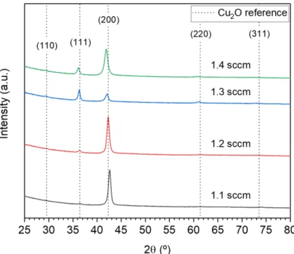
First, the LP set of films was analyzed. The respective data is represented in Figure 3.2, whereas the database references from the materials mentioned above are represented in Figure 3.3.
Figure 3.2 – XRD results of the LP set of Cu2O thin-films, consisting of four samples deposited using different O2 flow rates. The main peaks of Cu2O are represented by the dashed lines.
Analyzing the diffractograms, it is possible to observe that the main peaks of Cu2O are pre-sent, with no signs of peaks from other materials. This means that all the LP films are formed by Cu2O, independently of the O2 flow rate used. Nonetheless, except for the film deposited using a 1.2 sccm O2 flow rate, the peak position of the films is not the same when compared to the Cu2O reference. Comparing all the LP films, there is a visible trend when increasing the O2 flow rate used during the deposition: all the peaks are shifting to the left. Despite not presented here, both LP-SB and HP sets of films show the same behavior (Annex A), which is supported by literature. [16] The mentioned shift can be interpreted by Bragg’s law (2), which represents the condition where radiation waves are scattered by a crystalline solid, resulting in a constructive interference phenomenon.
2d sin θ = nλ (2)
In the equation, λ represents the wavelength of the incident radiation and θ its glancing angle; d is the distance between consecutive crystallographic planes and n is a positive integer. With Bragg’s law in mind, the peak shift to the left (smaller diffraction angles) seen in the films deposited using 1.3 and 1.4 sccm O2 flow rates can mean the films are under tensile strain (greater distance between crystallographic planes); the peak shift to the right (greater diffraction angles) seen in the film deposited using a 1.1 sccm O2 flow rate can mean that the film is under compres-sive strain (smaller distance between crystallographic planes). In summary, an increase of the O2 flow rate during the deposition process is inducing more tensile strain in the films, possibly due to the inclusion of more copper vacancies in the film. This results in the repulsion of neighboring oxygen anions which consequently leads to a lattice expansion. [17]
As the samples analyzed are thin-films, it is not possible to obtain absolute results on an eventual texturization. The volume illuminated by the X-ray decreases considerably with increasing diffraction angles, leading to a mismatch between the peak heights from the Cu2O reference and the films themselves. For that reason, only peak position has been analyzed so far. However, most
13
of the films show a preferential orientation in the (200) direction; the only exception is the most stoichiometric LP film, in which (111) and (200) directions are equally pronounced.
Besides the LP set of films, the most stoichiometric films from each set (LP-SB, LP and HP) were analyzed. The most stoichiometric HP film which was later heated at 100 °C for 24 hours (HP-heated) was also evaluated. It should be noted that the last-mentioned film had gold contacts deposited on it before the XRD measurement, which justifies the Au peaks in its diffractogram. All these results are represented in Figure 3.4.
As observed, the most stoichiometric films from the LP-SB, LP and HP sets show no signs of peaks from other materials besides Cu2O. The peak position of either the LP-SB or LP film is shifted to the left, which is more prominent on the first one. This can mean that both these two films are experiencing a tensile strain. On the other side, the HP film has its peaks shifted to the right, which can mean it is experiencing a compressive strain.
The HP-heated film also shows no peaks from other materials besides Cu2O. Furthermore, the diffractograms of both HP and HP-heated films have the same appearance (besides the obvi-ous Au peaks present on the HP-heated film). This is in line with the desired since the post-depo-sition heating treatment was supposed to change the properties of the grain boundaries, not the grains.
In spite of the most stoichiometric LP film showing no preferential orientation between (111) and (200) directions, the remaining films from the LP set have the (200) direction more pro-nounced. On the opposite, the most stoichiometric HP film have a preferential orientation in the
Figure 3.4 – XRD results of the most stoichiometric Cu2O thin-films from each set (LP-SB, LP and HP), including HP-heated film. The main peaks of Cu2O are represented by the dashed lines.
(111) direction, as the majority of the remaining films from the HP set. This shows a trend sup-ported by literature in which a lower deposition pressure promotes the (200) direction as the pref-erential orientation of the film, whereas a higher deposition pressure promotes the (111) direction. [18]
In a general way, the peaks are relatively broad which means the size of the grains in the film is in the nanometric range.
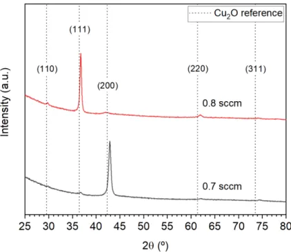
Below, the diffractograms of two specific films from the HP set are presented in Figure 3.5.
These two films, although they were deposited using similar O2 flow rates, have two different preferential orientations. The film deposited using a 0.7 sccm O2 flow rate has the (200) direction – which is the same as (100) – as preferential orientation, whereas the film deposited using a 0.8 sccm O2 flow rate is oriented preferentially in the (111) direction. The influence of this property is analyzed in a chapter ahead.
3.1.3. Scanning Electron Microscopy
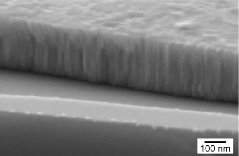
To complement the information obtained by transmittance spectroscopy and XRD, SEM was used to obtain images that were capable to show the polycrystalline structure of a Cu2O thin-film. Figure 3.6 displays a cross-section of one of the most stoichiometric Cu2O films.
Figure 3.5 – XRD results of two Cu2O thin-films from the HP set, deposited using 0.7 sccm and 0.8 sccm O2 flow rates. The main peaks of Cu2O are represented by the dashed lines.
15
First, this SEM image supports the thickness value obtained by profilometry. Considering a 265 nm thickness, the calculated sputtering deposition rate is 4.4 nm/min. In addition, the cross-section of the film shows its polycrystalline structure, namely the columnar shape of the grains.
3.1.4. X-Ray Photoelectron Spectroscopy
XPS was used to understand possible chemical composition differences between the films from the LP set deposited using different O2 flow rates. Figure 3.7 displays that data, specifically from the most important emissions: Cu 2p and O 1s.
Despite the different O2 flow rate used in each deposition, the results obtained are very similar among all the LP films, showing between 55% and 60% of oxygen, which indicates a strong CuO presence. It is worth referring that XPS is a technique that is only sensitive to the first 5-10 nm
Figure 3.6 – SEM cross-sectional image of the most stoichiometric LP Cu2O thin-film deposited on a silicon sub-strate.
Figure 3.7 – XPS data from (a) Cu 2p and (b) O 1s emissions relative to the LP set of films, consisting of four samples deposited using different O2 flow rates.
from the surface. For that reason, these results were already expected since Cu2O films oxidize easily while exposed to air and the XPS measurements were performed ex situ [2].
3.1.5. Atomic Force Microscopy and Conductivity Measurements
The last technique used to analyze the Cu2O thin-films was AFM/CAFM. These techniques allow obtaining information about the topography and local conductivity of a material in a very detailed way, which is useful due to the polycrystalline structure of these films. For a complemen-tary reason, conductivity measurements made by the van der Pauw method are also presented in this chapter.
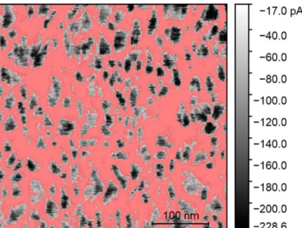
Among the different films, the average grain current (IG) was the factor that changed the most. To analyze that, Gwyddion’s potentialities were used. First, the current values were cor-rected by replacing the data that did not satisfy the 3σ criteria. Then, a mask that covers the less conductive part of the film (the grain boundaries) is applied. That mask contains the points with the 20% lower current values from the scale. Finally, the average current is calculated on the areas outside the mask (grains). In Figure 3.8 there is an example of the process used for all the films. The mask is represented in red.
Whereas the van der Pauw method can provide information about in-plane conductivity of the films (σIP), CAFM is able to provide information about out-of-plane conductivity of the grains (σOOP-G), which is calculated by Equation 3.
σOOP−G =
IG
VCAFM
∙tfilm
Atip (3)
17
In this formula, IG represents the average grain current obtained by the method explained above, VCAFM is the voltage used during CAFM measurements (2 V) and tfilm represents the thick-ness of the film. In addition, the AFM tip was considered a sphere with a 25 nm radius. Atip is the area of its bigger cross-section.
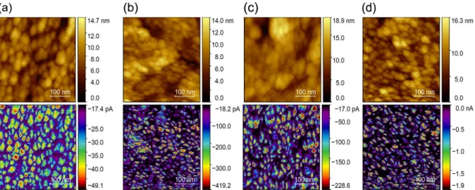
First, the LP set of films was analyzed. In Figure 3.9 it is possible to observe both topographic images and current maps of those films.
As observed in the topographic images, the polycrystalline structure of the films is immedi-ately visible. The grains have dimensions in the order of dozens of nanometers (supported by XRD and SEM) and the film roughness varies between 14 and 19 nm.
Regarding the current maps, it is important to refer that the range of currents measured is negative due to the voltage polarity used (-2 V). From now on, only absolute values will be referred. In these images, the polycrystalline structure of the films becomes more evident and there is an obvious difference in the conduction properties when comparing the grains and the grain bounda-ries. Conduction happens mostly inside the grains, whereas the grain boundaries have a negligible amount of current passing through. As observed, the lowest current value measured is very similar through all the films (around -17 pA), which leads to the conclusion that it could be a current offset of the equipment. Although the oxygen flow rate used during deposition does not change the fact that the grains are more conductive than the grain boundaries, it has an evident influence on the range of current values measured on the grains.
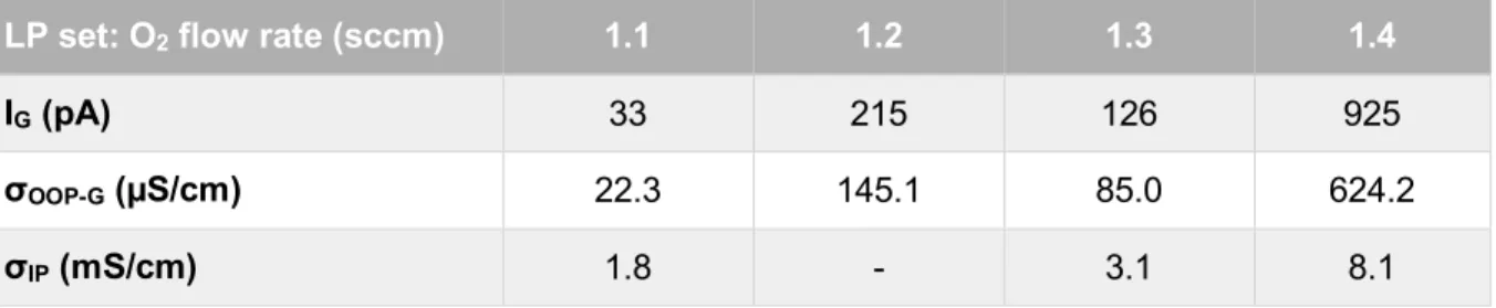
In Table 3.2, in-plane and out-of-plane conductivities of every LP film are compared.
Figure 3.9 – Topographic images and respective current maps of every Cu2O thin-film from the LP set, consisting of four samples deposited using different O2 flow rates: (a) 1.1 sccm, (b) 1.2 sccm, (c) 1.3 sccm and (d) 1.4 sccm.
Table 3.2 – IG, σOOP-G and σIP of every Cu2O thin-film from the LP set, consisting of four samples deposited using different O2 flow rates.
LP set: O2 flow rate (sccm) 1.1 1.2 1.3 1.4
IG (pA) 33 215 126 925
σOOP-G (µS/cm) 22.3 145.1 85.0 624.2
σIP (mS/cm) 1.8 - 3.1 8.1
There is a general trend in which the σOOP-G seems to get higher as the oxygen flow rate
used during the deposition of the film is higher. The film deposited using the lowest oxygen flow rate has the lowest σOOP-G (22.3 µS/cm), whereas the film deposited using the highest oxygen flow
rate has the highest σOOP-G (624.2 µS/cm), more than one order of magnitude above. For that
reason, it is possible to conclude that more oxidized films have greater σOOP-G. The film deposited
using a 1.3 sccm oxygen flow rate (the most stoichiometric one among LP films) is the only one that deviates from this trend, having a lower σOOP-G (85.0 µS/cm). This can be due to differences
on its preferential orientation compared to the other LP films (Figure 3.2).
In terms of σIP, one of the films could not be measured, though there seems to be a similar trend:
σIP t is also higher when the films are deposited using a higher O2 flow rate.
After comparing all the LP films, the most stoichiometric films deposited under the three different main conditions were compared. The most stoichiometric HP film which was later heated was also analyzed. The corresponding topographic images and current maps are displayed in Figure 3.10.
Comparing these results with the previous ones, there are no apparent differences regarding the fact that grains are still more conductive than the grain boundaries. This leads to the conclusion
Figure 3.10 – Topographic images and respective current maps of the most stoichiometric Cu2O thin-films from each set: (a) LP-SB, (b) LP and (c) HP, including (d) HP-heated film.
19
that this behavior does not get altered by using different chamber pressures, by applying a sub-strate bias, or even by heating the films. Nonetheless, average current values measured on the grains keep changing. Those values are presented in Table 3.3 in conjunction with out-of-plane and in-plane conductivities.
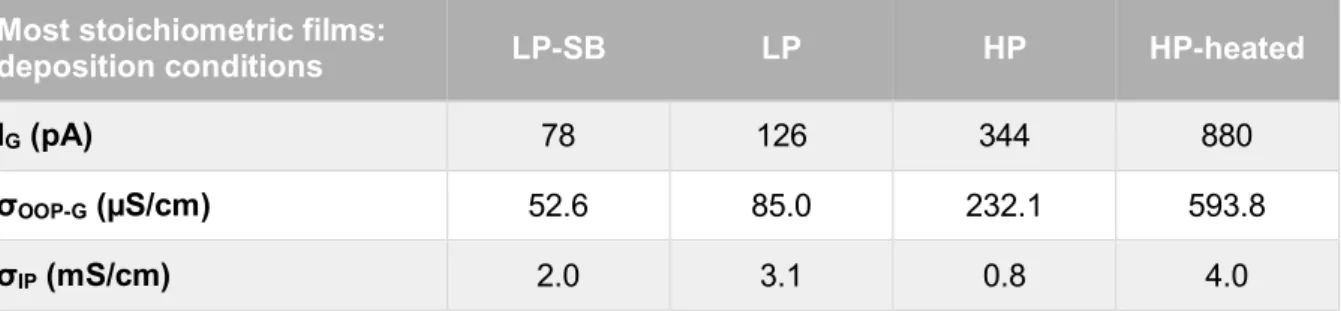
Table 3.3 – IG, σOOP-G and σIP of the most stoichiometric Cu2O thin-films from each set, including HP-heated film.
Most stoichiometric films:
deposition conditions LP-SB LP HP HP-heated
IG (pA) 78 126 344 880
σOOP-G (µS/cm) 52.6 85.0 232.1 593.8
σIP (mS/cm) 2.0 3.1 0.8 4.0
Comparing the most stoichiometric films from each set (LP-SB, LP, HP), it is possible to verify that σOOP-G increases in this order: LP-SB; LP; HP. Considering the same order, XRD
meas-urements showed that the films are experiencing an increased compressing strain (Figure 3.4). Since these films are all stoichiometric, copper vacancies cannot be the cause of the lattice ex-pansion. This leads to the conclusion that the improved conductivity can be related to the more compressed structure of the films, which may be associated with a higher densification state.
Relatively to the post-deposition heating treatment, it seems to increase the grain conduc-tivity since the HP-heated film has a σOOP-G significantly higher than the HP film. A heating treatment
oxidizes the films, similarly to what an increase of the O2 flow rate does. That is in line with the previous results in which more oxidized films had more conductive grains (Table 3.2).
In terms of σIP, it seems to follow the same trend as σOOP-G, except for the most stoichiometric
HP film, which has the lowest value among the analyzed films.
After observing that deposition conditions such as pressure, oxygen flow rate, substrate bias or even a post-deposition heating treatment do not influence the more-conductive-grain behavior, shorter depositions were made while keeping other factors constant. That way it was possible to understand if the thickness of the film had any influence on this behavior. In this case, the condi-tions used to obtain the most stoichiometric LP film were used. The respective topographic images and current maps are displayed in Figure 3.11.
Once more, the thickness of the films does not change the fact that the grains are more conductive than the grain boundaries. The average current values measured on the grains, as also out-of-plane and in-plane conductivities are shown in Table 3.4.
Table 3.4 – IG, σOOP-G and σIP of Cu2O thin-films deposited under the conditions of the most stoichiometric film from the LP set, consisting of four samples deposited during different times.
Most stoichiometric - LP set:
deposition time (min) 7.5 15 30 60
IG (pA) 438 324 198 126
σOOP-G (µS/cm) 37.0 54.7 66.8 85.0
σIP (mS/cm) 13.8 7.8 4.1 3.1
As verified, the increase of the film thickness slightly increases σOOP-G. On the opposite, σIP
decreases when the film thickness increases.
To understand the possible influence of the preferential orientation of the films on their elec-trical properties, the same two HP films discussed in the XRD chapter are analyzed here. Their respective topographic images and current maps are presented in Figure 3.12.
Figure 3.11 – Topographic images and respective current maps of Cu2O thin-films deposited under the same con-ditions as the most stoichiometric film from the LP set, consisting of four samples deposited during different times: (a) 7.5 minutes, (b) 15 minutes, (c) 30 minutes and (d) 60 minutes.
21
Once again, the grains are still more conductive than the grain boundaries. Information rel-ative to the average current measured on the grains and out-of-plane and in-plane conductivities are summarized in Table 3.5. Besides these results, resistivity measurements performed on the complete HP set of films, including data related to post-deposition heating treatments of different durations, are included in Annex B.
Table 3.5 – IG, σOOP-G and σIP of Cu2O thin-films from the HP set with different preferential orientations, consisting of two samples deposited using different O2 flow rates.
HP set: O2 flow rate (sccm) 0.7 0.8
Preferential Orientation (200) = (100) (111)
IG (pA) 15 344
σOOP-G (µS/cm) 10.1 232.1
σIP (mS/cm) 86.8 840.4
Analyzing these results, σOOP-G seems to be considerably higher on the (111)-oriented film than on the film oriented in the (100) direction, which is supported by literature. [11] Having in mind the columnar structure of the Cu2O thin-films observed by the cross-sectional SEM images (Figure 3.6), the interface between grains should have the same orientation as the surface. This assump-tion seems correct since σIP shows the same tendency as σOOP-G.
Figure 3.12 – Topographic images and respective current maps of Cu2O thin-films from the HP set with different preferential orientations, consisting of two samples deposited using different O2 flow rates: (a) 0.7 sccm and (b) 0.8 sccm.
Previously, emphasize was put on metallic particle formation and associated depletion of Cu2O to explain these differences in electrical conductivity. [7] However, the above indicates a strong contribution of the grain orientation to the current transport over its interfaces. The main conclusion is that (111) preferential orientation seems to promote a better charge carrier transport, compared to (100) direction.
Indeed, previous works showed that Cu2O thin-films that were (111)-oriented had increased grain boundary conductivity. [4], [8] The (111) interface also has a higher tendency to oxidize. [9]
To better investigate the influence of the preferential orientation of the films, Kelvin probe force microscopy (KPFM) measurements were performed. [19] However, the images do not lead to any conclusion due to the small size of the grains compared to the resolution allowed by the equipment. Those results are present in Annex C.
All the images above were obtained by applying a -2 V voltage to the films. Different voltage values were tested, as also different polarities. In Figure 3.13 there is an example of an image obtained by changing the voltage polarity in the middle of the process.
There are no visible differences regarding the topographic image. One advantage of using a -2V voltage compared to a +2 V voltage is the better contrast obtained in the current map be-tween the grains and the grain boundaries. Although, that does not change the behavior of grains being more conductive compared to the grain boundaries.
A different AFM equipment was also tested to verify if it would show different results. Both the topographic image and the current map of one of the most stoichiometric films are presented in Figure 3.14.
Figure 3.13 – (a) Topographic image and (b) respective current map of the LP film deposited using a 1.1 sccm O2 flow rate. The top half of either image was obtained by using a -2 V voltage and the bottom half using a +2 V voltage.
23
The images above are visibly clearer and more stable than the images of the same film made with the MFP-3D-SA system (Figure 3.10 (c)). Both images show no drift and the contrast between the grains and the grain boundaries is significantly better, mainly in the current map. However, the grains are still more conductive than the grain boundaries, which allows concluding that the equipment has no influence on this behavior.
3.2.
Particles
3.2.1. Scanning Electron Microscopy
The shape of the particles was the most important property to be assured, so SEM was the first technique used. The process was optimized, and the particles were grown into the desired shapes. Figure 3.15 shows the results obtained in one synthesis (1st synthesis) and Figure 3.16 shows the results obtained in a posterior synthesis (2nd synthesis).
Figure 3.14 – (a) Topographic image and (b) respective current map of the most stoichiometric Cu2O thin-film from the HP set obtained by Cypher S.
In the 1st synthesis, particles of either shape had a similar size, around 400 nm. Although, cubic particles showed a greater size dispersion compared to the octahedral ones. In the 2nd syn-thesis, the shape of both cubic and octahedral particles was not so perfect as before. Both showed a considerable size dispersion and the presence of agglomerates. Besides that, cubic particles became smaller (around 200 nm) and octahedral particles became bigger (around 700 nm) when compared to the 1st synthesis.
Figure 3.15 – SEM images of (a) cubic and (b) octahedral particles obtained in the 1st synthesis.
25
3.2.2. X-Ray Diffraction
To identify other possible phases besides Cu2O that could be present in the particles, XRD measurements were performed. The diffractograms relative to the particles obtained in the 1st syn-thesis are shown in Figure 3.17.
Diffractograms from both shapes of particles are identical and represent an almost-perfect match with the Cu2O pattern. Only the octahedral particles show a slight peak shift to the right, which can suggest the structure is under a compressive strain. In terms of peak height, both par-ticles fit the pattern precisely. Observing the width of the peaks, the immediate conclusion is that the crystallite size must be bigger than what is observed in the films (Figure 3.4). Probably, each particle consists on a single crystalline domain.
3.2.3. Energy Dispersive X-Ray Spectroscopy
EDS allows obtaining information about the chemical composition of the particles. Cubic and octahedral particles from both syntheses were analyzed and the results are displayed in Table 3.6.
Table 3.6 – Oxygen content of cubic and octahedral particles from both syntheses, obtained by EDS.
Oxygen content (%) 1st synthesis 2nd synthesis
Cubic 16.6 29.4
Octahedral 30.2 24.0
Figure 3.17 – XRD results from cubic and octahedral particles obtained in the 1st synthesis. The main peaks of Cu2O are represented by the dashed lines.
The EDS results obtained from the particles, although not showing a 2:1 Cu/O proportion, all suggest a stronger presence of copper compared to oxygen, with a signal at least twice more intense. Independently of the particle shape, the smaller particles (cubic – 2nd; octahedral – 1st), which have a superior surface/body ratio, show a stronger oxygen presence than the bigger ones (respectively: cubic – 1st; octahedral – 2nd), which leads to the conclusion that possibly the surface of the particles is more oxidized than their inside. XPS measurements were also performed, none-theless, they did not provide any consistent conclusion. Those results are present in Annex D.
3.2.4. Atomic Force Microscopy
To understand the influence of the facets on the conductive properties of Cu2O, several AFM/CAFM measurements were performed on particles of both shapes.
The synthesis was still unoptimized when the first images were tested. A topographic image and a current map of unoptimized octahedral particles can be observed in Figure 3.18. The system used was a Cypher S and the current map was obtained with no voltage applied to the substrate.
After optimizing the synthesis, MFP-3D-SA system was used to obtain similar images of the octahedral particles from the 1st synthesis. The process to obtain images with good resolution took dozens of hours which promoted some issues related to drift and loss of contact with the surface. For that reason, only the low-resolution images present in Figure 3.19 could be obtained.
Figure 3.18 – (a) Topographic image and (b) respective current map of unoptimized octahedral particles obtained by a Cypher S system.
27
Posteriorly, it was possible to analyze the same particles with a different equipment, a
Nano-Observer system. The respective topographic images and resistivity maps are shown in Figure
3.20.
Figure 3.20 – Topographic images and respective resistivity maps of (a) cubic and (b) octahedral particles from the 1st synthesis. Images obtained by a Nano-Observer system.
Images from Figure 3.18 and Figure 3.19 do not have enough quality that allows taking any conclusion. Figure 3.20, despite not showing the exact shape of the particles on the topographic images, seems to show some differences in the resistivity. Cubic particles seem to be more resis-tive than the octahedral ones, which is in line with the literature. [11]
Figure 3.19 – (a) Topographic image and (b) respective current map of octahedral particles from the 1st synthesis obtained by a MFP-3D-SA system.
29
4. Conclusions and Future Perspectives
In this work, Cu2O thin-films were successfully produced by reactive sputter deposition. After altering several conditions, such as deposition pressure, oxygen flow rate, substrate bias, deposi-tion time and post-deposideposi-tion heating treatment, films with more conductive grain boundaries could not get achieved. Instead, Cu2O films with more conductive grains were obtained.
Transmittance spectroscopy allowed measuring the bandgap of the most stoichiometric Cu2O films. The value obtained was 2.57 eV, higher than the 2.17 eV referenced, nonetheless, it was expected due to limitations of this technique.
XRD measurements showed that the films experience more tensile strain as their oxygen content increases due to the presence of copper vacancies. Besides that, XRD shows that different deposition pressures and the substrate bias modify the crystallographic lattice, possibly related to differences in the densification state of the films.
SEM revealed the columnar growth of the grains inside the film, whereas XPS confirmed the easy oxidation of the Cu2O thin-films when exposed to air.
AFM/CAFM, in conjunction with conductivity measurements, showed that the films with greater oxygen content are more conductive; when comparing films with the same oxygen content, it seems that the more compressed films are more conductive. A post-deposition heating treatment oxidizes the films, which increases their conductivity. Curiously, two films deposited under the same conditions with similar oxygen contents showed very different electrical properties. This is thought to be related to the preferential orientation of the films: the film preferentially oriented in the (111) direction is significantly more conductive than the (100)-oriented.
Besides the films, particles of cubic and octahedral shapes were successfully produced from solution. XRD showed that the particles were made from Cu2O, and EDS, although not providing an exact Cu/O ratio of 2:1, supported those results.
AFM/CAFM measurements on the particles proved to be extremely difficult to perform. De-spite the different approaches that were made to prepare the particles and the different systems tested, the steep topography of the samples was a constant issue. However, one of the measure-ments seems to indicate that octahedral particles – (111) facets – are more conductive than cubic ones – (100) facets.
To conclude, preferential orientation of grain interfaces in a film seems to be a factor with some importance on the electrical properties of the film. Undoubtedly, XRD is a good technique to be used when producing thin-films.
31
References
[1] H. A. Al-Jawhari, “A review of recent advances in transparent p-type Cu2O-based thin film transistors,” Mater. Sci. Semicond. Process., vol. 40, pp. 241–252, 2015.
[2] J. Deuermeier et al., “Highly conductive grain boundaries in copper oxide thin films,” J. Appl.
Phys., vol. 119, no. 23, 2016.
[3] Y. S. Lee, M. T. Winkler, S. C. Siah, R. Brandt, and T. Buonassisi, “Hall mobility of cuprous oxide thin films deposited by reactive direct-current magnetron sputtering,” Appl. Phys. Lett., vol. 98, no. 19, p. 192115, 2011.
[4] J. Deuermeier et al., “Visualization of nanocrystalline CuO in the grain boundaries of Cu2O thin
films and effect on band bending and film resistivity,” APL Mater., vol. 6, p. 096103, 2018. [5] C. Das et al., “Effect of Grain Boundary Cross-Section on the Performance of Electrodeposited
Cu2O Photocathodes,” J. Phys. Chem. C, vol. 122, no. 3, pp. 1466–1476, 2018.
[6] J. Deuermeier, H. Liu, L. Rapenne, R. Martins, and D. Mu, “Visualization of nanocrystalline CuO in the grain boundaries of Cu 2 O thin films and effect on band bending and film resistivity,” APL
Mater., vol. 096103, 2018.
[7] S. Siol et al., “Band Alignment Engineering at Cu2O/ZnO Heterointerfaces,” ACS Appl. Mater.
Interfaces, vol. 8, no. 33, pp. 21824–21831, Aug. 2016.
[8] H. Liu et al., “The Role of Humidity in Tuning the Texture and Electrical Properties of Cu 2 O Thin Films Deposited via Aerosol-Assisted CVD,” Adv. Mater. Interfaces, vol. 6, no. 3, pp. 1–10, 2019.
[9] Y. Su, H. Li, H. Ma, J. Robertson, and A. Nathan, “Controlling Surface Termination and Facet Orientation in Cu2O Nanoparticles for High Photocatalytic Activity: A Combined Experimental and Density Functional Theory Study,” ACS Appl. Mater. Interfaces, vol. 9, no. 9, pp. 8100– 8106, 2017.
[10] Y. B. Vogel, J. Zhang, N. Darwish, and S. Ciampi, “Switching of current rectification ratios within a single nanocrystal by facet-resolved electrical wiring,” ACS Nano, vol. 12, no. 8, pp. 8071– 8080, 2018.
[11] C. S. Tan, S. C. Hsu, W. H. Ke, L. J. Chen, and M. H. Huang, “Facet-dependent electrical conductivity properties of Cu2O crystals,” Nano Lett., vol. 15, no. 3, pp. 2155–2160, 2015. [12] C. H. Kuo and M. H. Huang, “Facile synthesis of Cu2O nanocrystals with systematic shape
evolution from cubic to octahedral structures,” J. Phys. Chem. C, vol. 112, no. 47, pp. 18355– 18360, 2008.
[13] D. F. Zhang, H. Zhang, L. Guo, K. Zheng, X. D. Han, and Z. Zhang, “Delicate control of crystallographic facet-oriented Cu2O nanocrystals and the correlated adsorption ability,” J.
Mater. Chem., vol. 19, no. 29, pp. 5220–5225, 2009.
[14] J. Deuermeier, “Origins of limited electrical performance of polycrystalline Cu2O thin-film transistors” (Doctoral dissertation). Universidade Nova de Lisboa, Portugal; Technische Universität Darmstadt, Germany. 2016.
[15] B. K. Meyer et al., “Binary copper oxide semiconductors: From materials towards devices,” Phys.
Status Solidi B, vol. 249, no. 8, pp. 1487–1509, Aug. 2012.
[16] H. Zhu, J. Zhang, X. Lan, C. Li, T. Wang, and B. Huang, “Photo-catalytic activity of Cu2O films with various crystal structures prepared by DC reactive magnetron sputtering,” Mater. Sci.
Forum, vol. 610–613, pp. 293–298, 2009.
[17] J. Deuermeier, J. Gassmann, J. Brötz, and A. Klein, “Reactive magnetron sputtering of Cu2O:
Dependence on oxygen pressure and interface formation with indium tin oxide,” J. Appl. Phys., vol. 109, no. 11, p. 113704, 2011.
[18] Y. Wang, “Controllable growth , microstructure and electronic structure of copper oxide thin films" (Doctoral dissertation). Université de Lorraine, France. 2018.
[19] N. Nicoara et al., “Direct evidence for grain boundary passivation in Cu(In,Ga)Se2 solar cells through alkali-fluoride post-deposition treatments,” Nat. Commun., vol. 10, no. 1, pp. 1–8, 2019.
33
Annexes
Annex A
XRD results of every film from: (a) HP set, consisting of five samples deposited using different O2 flow rates; (b) LP-SB set, consisting of three samples deposited using different O2 flow rates. The main peaks of Cu2O are rep-resented by the dashed lines.
Annex B
Resistivity values (Ω cm) measured by the van der Pauw method of every film from the HP set. Influence of post-deposition heating treatment of different durations.
0.6 sccm 0.7 sccm 0.8 sccm 0.9 sccm 1.0 sccm 0 h 43 11528 1190 42 15 6 h 1222 16934 - 35 17 12 h 6758 10680 334 46 19 24 h 13727 36305 251 46 19
Annex C
Annex D
KPFM results: (a) topographic image and (b) contact potential difference map of a Cu2O thin-film from the HP set deposited using a 0.7 sccm O2 flow rate.
XPS data from (a) Cu 2p and (b) O 1s emissions relative to cubic and octahedral particles obtained in 1st and 2nd syntheses.