Abstract—In this paper, the effect of temperature and doping concentration on the breakdown voltage, multiplication gain and noise factor of abrupt junction avalanche photodiodes has been investigated for hole- and electron-initiated processes. Temperature-dependent models have been developed including the temperature variation of impact ionization coefficients, bandgap, intrinsic carrier concentration, dielectric constant and built-in-potential. The developed models have been used to study the impact of temperature and doping concentration on the device characteristics. The models can be implemented in simulation tools, in order to study avalanche photodiode-based systems including thermal effects.
Index Terms—Avalanche photodiode, multiplication
gain,noise factor, breakdown voltage, temperature sensitivity.
I. INTRODUCTION
valanche photodiodes (APDs) are widely used in several applications such as instrumentation, nuclear medicine and aerospace, thanks to their high speed and high sensitivity [1-2]. The increase in photodetectors market is fostering the development of new designs based on the optimization of cost/efficiency ratio for larger scale mass production. In CMOS technology era, the avalanche photodiode is considered as promising candidate to meet the need for optical sensors with improved speed and detection efficiency. This is mainly due to the low manufacturing costs of the silicon APDs, their compatibility with CMOS monolithic integration, and their excellent optical properties. On the other hand, the integration of efficient low-noise photodiodes in standard CMOS technology requires the introduction of custom doping implantation, which is necessary to improve temperature stability, reduce dark current and excess noise. Therefore, in order to get a global view of avalanche photodiode performance, new models, designs and optimization approaches are necessary for the comprehension of the fundamentals device characteristics. In this context, several studies have been proposed to investigate the avalanche photodiode and to gain a better
T. Bendib is with DII, University of Trento, Via Sommarive, 9, 38123 Trento, Italy, and Laboratory of Advanced Electronic, University of Batna, 05000, Algeria (e-mail: [email protected]).
F. Djeffal is with the Laboratory of Advanced Electronic, Department of Electronics, LEPCM, University of Batna, 05000, Algeria (e-mail: [email protected], [email protected]).
L. Pancheri is with DII, University of Trento, Via Sommarive, 9, 38123 Trento, Italy,(e-mail: [email protected]).
G.F. Dalla Betta is with DII, University of Trento, Via Sommarive, 9, 38123 Trento, Italy, (e-mail: [email protected]).
understanding of its behavior [3-5].
Several analytical/experimental works have been recently published to study the impact of doping level on the performance of APD [6–7]. In addition, there are many research papers available on the temperature effects on APDs [9–10]. However, it is missing a careful analysis of the impact of doping concentration on the temperature sensitivity of APD performance, which has been presented in this paper. Temperature-dependent models have been incorporated for all the relevant physical quantities: impact ionization coefficients, bandgap, intrinsic carrier concentration, dielectric constant and built-in-potential.
II. MODEL FORMULATION
Based on McIntyre theory and a one-dimensional analysis, the multiplication gain M and the excess noise factor F for carriers generated at x are expressed as [11]:
'exp 1
exp )
(
0
dx dx dx x
M
W
x W
W
x
(1)
) (
1 ) ( 2 ) ( 2 )
( 0
2
x M
dx x M W
M x
F
W
(2) whereand are the electron and hole impact ionization coefficients and W is the space-charge region width. and are dependent on temperature and applied electric field and expressed by the Okuto-Crowellmodel as [12,13]:
n
E T B T
A N
N
( )exp ( ) (3)
p
E T B T
A P
P
( )exp ( ) (4) where T is absolute temperature and E is the electric field. The parameters AN, AP, BN and BP are a function of
temperature used to parameterize the temperature dependence of α and β, as well as the electric field dependence. AN, AP, BN and BPare expressed as [12,13]
npp n p n P
N T
A ,
300))E -(T c (1
a , ,
,
(5)
b , (1 d , (T-300)),P np np
N T
B (6)
Impact of Temperature and Doping
Concentration on Avalanche Photodiode
Characteristics
T. Bendib, L. Pancheri, F. Djeffal and G.-F. Dalla Betta
A
Proceedings of the World Congress on Engineering 2014 Vol I, WCE 2014, July 2 - 4, 2014, London, U.K.
ISBN: 978-988-19252-7-5
ISSN: 2078-0958 (Print); ISSN: 2078-0966 (Online)
These models are suitable for bulk ionization coefficients over the electric field range of 105–106 V · cm−1 and the temperature range of 15°K–500 °K [12].
The breakdown voltage, that is theoretically defined as the voltage when the multiplication gain approaches infinity, can be calculated as an extrapolation of (1).
In order to study the impact of doping concentration on the temperature sensitivity of the device, temperature dependency of various semiconductor parameters like bandgap (Eg), intrinsic carrier concentration (ni), dielectric constant of silicon (si) and built-in-potential (Vbi) have been implemented, as given below [13]:
3 2 300 ) 300 ( ) (
N T
T
NC C (7)
3 2 300 ) 300 ( ) (
N T
T
NV V (8)
g g g g g E T T E E T E 2 2 300 300 E + ) 300 ( )
( (9)
kT T qE T N T N T
ni C V g
2 ) ( exp ) ( ) ( )
( (10)
) ( log ) ( 2 T n N N q kT T V i B A
bi (11)
04 10 3 . 1 1 4 . 11 ) ( T T
si (12)
where: 3 19 10 8 . 2 ) 300
( cm
NC 3 19 10 1.04 ) 300
( cm
NV .
eV
Eg(300)1.08 ,Eg 4.7310-4eV/K,Eg 636K, These parameters are used to calculate the electric field distribution in abrupt junction n+/p, which is given by:
) ( 1 ) ( ) ( T W x T E x
E M (13)
where
si B M T W qN E ) ( (14)
V T V N qN N N T T W bi B A B Asi
2 ( ) ( )
)
( (15)
III. RESULTS AND DISCUSSION
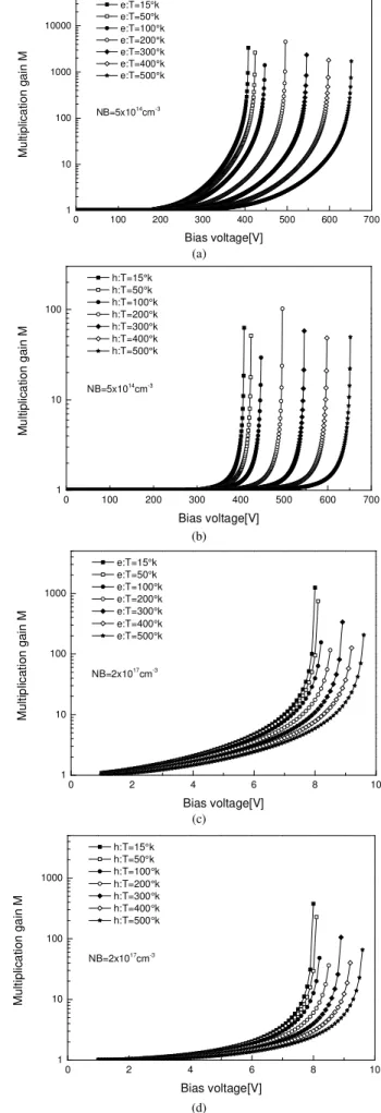
In this section, the breakdown voltage, the multiplication gain and the excess noise factor are calculated using Eqs. (1,2) in order to evaluate the APD performances at different temperature and substrate doping levels. The electron and hole initiated multiplication gain obtained with our combined model, predicted for different temperatures between T = 15°K and 500°K, are illustrated in Figure 1. As expected, this figure shows that, since electron ionization coefficients are larger than hole coefficients in Si devices, the electron-initiated multiplication gain is larger than that the hole initiated process. However, this difference reduces by increasing the multiplication region doping concentration, as a result of the reduction of ionization coefficient ratio at high electric fields.
0 100 200 300 400 500 600 700
1 10 100 1000 10000 M u lt ip lic a ti o n g a in M Bias voltage[V] e:T=15°k e:T=50°k e:T=100°k e:T=200°k e:T=300°k e:T=400°k e:T=500°k NB=5x1014 cm-3 (a)
0 100 200 300 400 500 600 700
1 10 100 M u lt ip lic a ti o n g a in M Bias voltage[V] h:T=15°k h:T=50°k h:T=100°k h:T=200°k h:T=300°k h:T=400°k h:T=500°k NB=5x1014 cm-3 (b)
0 2 4 6 8 10
1 10 100 1000 M u lt ip lic a ti o n g a in M Bias voltage[V] e:T=15°k e:T=50°k e:T=100°k e:T=200°k e:T=300°k e:T=400°k e:T=500°k NB=2x1017 cm-3 (c)
0 2 4 6 8 10
1 10 100 1000 Mu lt ip lic a ti o n g a in M Bias voltage[V] h:T=15°k h:T=50°k h:T=100°k h:T=200°k h:T=300°k h:T=400°k h:T=500°k NB=2x1017 cm-3 (d)
Fig. 1. Electron and hole initiated gain versus bias voltage for APD at various temperatures in the range of 15°K < T < 500°K (a) and (b) with NB=5×1014cm-3, (c) and (d) with NB=2×1017cm-3. The electron and hole initiated processes are designated by e and h, respectively.
Proceedings of the World Congress on Engineering 2014 Vol I, WCE 2014, July 2 - 4, 2014, London, U.K.
ISBN: 978-988-19252-7-5
ISSN: 2078-0958 (Print); ISSN: 2078-0966 (Online)
Moreover, the ratio between the electron and hole initiated characteristics is larger as the bias voltage approaches the breakdown value for both low and high doping levels. This ratio, close to breakdown voltage, becomes smaller at high temperatures for low substrate doping level (Figure2.a) and almost saturates at the value of approximately 3.2 for high substrate doping level (Figure2.b).
0 100 200 300 400 500 600 700
0 10 20 30 40 50 60
M
u
lt
ip
lic
a
ti
o
n
r
a
ti
o
M
e
/M
h
Bias voltage[V]
T=15°K T=50°K T=100°K T=200°K T=300°K T=400°K T=500°K
NB=5x10¹⁴
cm-3
(a)
0 2 4 6 8 10
1 2 3 4
M
u
lt
ip
lic
a
ti
o
n
r
a
ti
o
M
e
/M
h
Bias voltage[V]
T=15°k T=50°k T=100°k T=200°k T=300°k T=400°k T=500°k
NB=2x1017cm-3
(b)
Fig. 2. Ratioof electron and hole initiated gain versus bias voltage for APD at various temperatures in the range of 15°K < T < 500°K (a) with NB=5×1014cm-3, (b) with NB=2×1017cm-3.
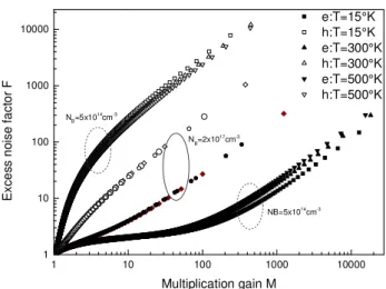
Fig. 3 shows the excess noise factor versus multiplication gain for both electron and hole initiated process calculated for the investigated APDs with different doping concentration, at three temperature values 15°K, 300°K and 500°K.
This figure illustrates that the increase in the ambient temperature reduces the excess noise for a given doping concentration NB in the case of pure electron injection,
while F increases in the case of pure hole injection. This behavior results from a decrease of ionization rates ratio at increasing temperatures. Furthermore, as can be observed from Figure 3, at a concentration of NB=2×1017cm-3, the
electron and hole initiated processes are less sensitive to the temperature variations, and also their corresponding excess noise factor. As a result APDs with larger multiplication doping levels are more stable with respect to ambient temperature variations.
1 10 100 1000 10000
1 10 100 1000 10000
e:T=15°K h:T=15°K e:T=300°K h:T=300°K e:T=500°K h:T=500°K
E
x
c
e
ss
n
o
is
e
f
a
c
to
r
F
Multiplication gain M NB=5x10¹⁴
cm-3
NB=5x10 14cm-3
NB=2x10 17cm-3
Fig. 3. Excess noise factor F as a function of the electron and hole
multiplication gain at various temperatures in the range of 15°K < T < 500°K with NB=5×1014cm-3 and NB=2×1017cm-3. The electron
and hole initiated processes are designated by e and h, respectively.
Figure 4 shows the temperature dependence of breakdown voltage for doping concentration range of 5×1014cm-3 < NB<
2×1017cm-3.
This figure demonstrates that an increase in ambient temperature causes the breakdown voltage to increase for a given substrate doping concentration. The obtained behavior is due to an increase of the phonon population with temperature. Therefore, a higher electric field and applied voltage are required to reach breakdown in order to overcome the increased carrier cooling caused by phonon scattering[14]. It can be observed that the temperature coefficient is reduced by increasing the doping concentration, thanks to the reduction of the multiplication region width [15]. As shown in Figure 4, an approximately linear temperature dependence is found for all doping concentrations in the considered range, where the breakdown voltage variation is strongly reduced as a function of temperature for high doing concentration values. At the highest concentration values considered in Figure 4, it is to note that the breakdown voltage saturates at low temperatures, probably because of the corresponding saturation in the phonon population. On the contrary, the impact of temperature on breakdown voltage value is larger for low doping concentrations. Therefore, the device immunity against the temperature variation is improved by increasing the intrinsic region doping. However, the high doping values can degrade other device characteristics like multiplication gain and excess noise factor, especially electron-initiated process.
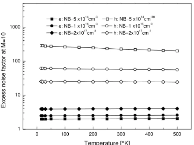
The impact of temperature on the noise factor, with various doping levels 5×1014 cm-3, 1×1016cm-3 and 2×1017cm-3 was evaluated by extracting the noise factor values at a fixed multiplication gain M=10 for both hole and electron pure injection. As shown in Figure 5, a linear temperature dependence is found for both pure electron and pure hole injection for low and high doping concentration levels.
Proceedings of the World Congress on Engineering 2014 Vol I, WCE 2014, July 2 - 4, 2014, London, U.K.
ISBN: 978-988-19252-7-5
ISSN: 2078-0958 (Print); ISSN: 2078-0966 (Online)
0 100 200 300 400 500 70
80 90 100 110 120
Vb
d
(T
)/
Vb
d
(3
0
0
°K
)(
%
)
Temperature [°K] NB=5 x10¹⁴
cm-3
NB=1 x10¹⁵
cm-3
NB=1 x1016cm-3 NB=1 x1017cm-3 NB=2 x10¹⁷
cm-3
Fig. 4. APD avalanche breakdown voltage Vbd normalized to the 300°K value as a function of temperature obtained by our combined model with various doping levels.
As noticed in Figure 5, for all the substrate doping concentrations, excess noise factor increases slightly with temperature for pure electron injection and decreases for pure hole injection. Moreover, at an operating temperature, the noise factor is reduced (increased) by increasing of doping level in the multiplication region for pure hole injection (pure electron injection) respectively.
0 100 200 300 400 500
1 10 100 1000
e: NB=5 x10¹⁴
cm-3
h: NB=5 x10¹⁴
cm-30
e: NB=1 x10¹⁶
cm-3
h: NB=1 x10¹⁶
cm-3
e: NB=2x10¹⁷
cm-3
h: NB=2x10¹⁷
cm-3
E
x
c
e
s
s
n
o
is
e
f
a
c
to
r
a
t
M
=
1
0
Temperature [°K]
Fig. 5. Excess noise factor F at a gain M=10 as a function of temperature. Simulation obtained by our combined model for pure electron and pure hole injection with various doping levels. The electron and hole initiated processes are designated by e and h, respectively.
IV. CONCLUSION
In this paper, a temperature-dependent model for the simulation of breakdown voltage, multiplication gain and noise factor in silicon APDs is presented. It is found that increasing of doping level in the APD multiplication region reduces the temperature coefficient of gain and noise. Moreover, the temperature sensitivity of breakdown voltage is more pronounced for low doping concentration. It is to note that this investigation can be extended to 2D and 3D simulation domains and applied to different semiconductor materials (for example: SiGe). As local field models are known to over-estimate the APD excess noise factor [11], the value of F provided by the proposed model can be considered as a worst-case estimation. Nonlocal models
should be implemented to obtain more accurate excess noise factor estimation.
REFERENCES
[1] M. Moszyński, M. Szawlowski, M. Kapusta and M. Balcerzyk,
“Large area avalanche photodiodes in scintillation and X-rays detection,” Nucl. Instr. Meth. Phys. Res. A, Vol. 485, pp. 504-521, 2002.
[2] A. Biber, P. Seitz and H. Jäckel, “Avalanche photodiode image sensor in standard BiCMOS technology,” IEEE Trans. Electron Devices, Vol. 47, pp. 2241–2243, 2000.
[3] A. Rochas, M.Gösch, , A. Serov, P.A. Besse , R.S. Popovic, T. Lasser and R. Rigler, “Low-Noise Silicon Avalanche Photodiodes Fabricated in Conventional CMOS Technologies,” IEEE Trans. Electron Devices, Vol. 49, pp. 387-394, 2002.
[4] L. Pancheri, M. Scandiuzzo, D. Stoppa and G.-F. DallaBetta, “Low-Noise Avalanche Photodiode in Standard 0.35-μm CMOS Technology,” IEEE Trans. Electron Devices, Vol. 55, pp. 457-461, 2008.
[5] G.M. Williams, M. Compton, D.A. Ramirez, M.M. Hayat, A.S. Huntington, “Multi-Gain-Stage InGaAs Avalanche Photodiode With Enhanced Gain and Reduced Excess Noise,” IEEE Trans. Electron Devices, Vol. 1, pp. 54 - 65, 2013.
[6] M. Kanishka and D. N. Ranjan, “Gain and bandwidth analysis and comparison for gallium arsenide and silicon avalanche photodiodes with very thin multiplication layer,” Optical Engineering, Vol. 52, pp. 54001, 2013.
[7] L. Pancheri, T. Bendib, G.-F. Dalla Betta and D. Stoppa, “Design and characterization of Avalanche Photodiodes in submicron CMOS technologies,”Pr oc. SPIE 8982 (Optical Components and Mater i als XI), 898211, 2014.
[8] K. Ogasawara, S. Livi and D.J. McComas, “Temperature dependence of the thin dead layer avalanche photodiode for low energy electron measurements,”Nucl. Instr. Meth. Phys. Res. A, Vol. 611, pp. 93–98, 2009.
[9] Y-S. Chung, Il-Y. Park, Y-Ik. Choi, S-K. Chung, “Temperature dependent effective ionization coefficient for Si,” Microelectronic Engineering, Vol. 51–52, pp. 535–540, 2000.
[10] S. Masudy-Panah, M.K. Moravvej-Farshi and M. Jalali, “Temperature dependent characteristics of submicron GaAs avalanche photodiodes obtained by a nonlocal analysis,” Optics Communications, Vol. 282, pp. 3630–3636, 2009.
[11] R.J. McIntyre, “A new look at impact ionization-Part I: A theory of gain, noise, breakdown probability, and frequency response,” IEEE Trans. Electron Devices, Vol. 46, pp. 1623-1631, 1999.
[12] Y. Okuto and C.R. Crowell, “Threshold energy effect on avalanche breakdown voltage in semiconductor junctions,” Solid-State Electronics, Vol. 18, pp. 161-168, 1975.
[13] Atlas user’s manual, SILVACO TCAD, 2008.
[14] D. J. Massey, J. P. R. David, and G. J. Rees, “Temperature dependence of impact ionization in submicrometer silicon devices,” IEEE Trans. Electron. Devices, Vol. 53, pp. 2328-2334, 2006. [15] P. Agarwal, M. J. Goossens, V. Zieren, E. Aksen, and J. W.
Slotboom, “Impact ionization in thin silicon diodes,” IEEE Electron Device Letters, Vol. 25, no. 12, pp. 807–809, 2004.
Proceedings of the World Congress on Engineering 2014 Vol I, WCE 2014, July 2 - 4, 2014, London, U.K.
ISBN: 978-988-19252-7-5
ISSN: 2078-0958 (Print); ISSN: 2078-0966 (Online)