Abstract—Recent studies proved that certain electronic active
circuits are capable to exhibit simultaneously a negative group delay (NGD) and amplification in microwave frequency bands. One of the simplest topologies generating this counterintuitive NGD function effect is formed by a series RLC-network in cascade with a transistor. By using this cell, similar to the classical electronic functions, dual-band NGD microwave devices with loss compensation possibility can be designed. Theoretic demonstrations concerning the theory of the NGD circuit considered are presented. The dual-band NGD concept feasibility is concretely illustrated by an example of EM/circuit co-simulations. So, in frequency domain, dual-band NGD with minimal values of about –1 ns was observed simultaneously within two frequency bands centered at about 1.05 GHz and 2.05 GHz. To highlight the functioning of the hybrid device considered, time-domain analysis showing the RF/microwave signal advancement is performed. As application, the concept investigated can be envisaged for data synchronization in multi-channel wireless communication systems eventually degraded by undesired EMI effects.
Index Terms— Dual-band device, microwave active circuit, negative group delay (NGD), signal synchronization.
I. INTRODUCTION
Nowadays, global take-up of mobile terminals and personal computers in daily human way of life
involves the development of more and more reliable electronic circuitry. Substantially, one of most
expanded outstanding technological consequences is the introduction of several applications and
functionalities in communicating cellular as the case of IEEE 802 (WLAN/WiFi, WiMAX/WiBRO).
Nevertheless this spectacular progress is accompanied by certain technical issues as the saturation of
usable channel spectrum which happens currently with certain European operators [1].
Facing to this roadblock, higher and adaptative modulation rate, and cross-pole interference
cancellation technique have been proposed. In addition, for the military and public safeties, various
wireless communication architectures as phased-array subsystems [2-3] and typically multi-band
microwave circuits using, in particular, the negative group delay (NGD) effect [4-13] were recently
put forward. Usually, electronic devices considered for the classical electronic functions (filter,
amplification, phase shifter…) were designed only according to the specifications based on the
An FET-Based Microwave Active Circuit with
Dual-Band Negative Group Delay
Blaise Ravelo1
1
IRSEEM, EA 4353 at Graduate School of Engineering ESIGELEC, Av. Galilée, BP 10024, 76801 Saint Etienne du Rouvray Cedex, France.
E-mail: [email protected]
Serge De Blasi2
²UNIVERSSEL (Univers des Services d'Enseignement et de Laboratoire), 6 rue Casse-La-Foi, 29290 Saint-Renan, France.
magnitude and phase of the communication parameters. However, with the increase of data rate, it
was found that relevant values of signal delay or group delay seem also necessary for example, to
insure the signal synchronization in RF/digital links like GPS and WiMAX system [14]. Most
importantly, problems caused by signal distortion related to the group delay flatness default were also
met in particular, for the impulse radio system [15]. Meanwhile, well-synchronized signals are
required to maintain the system coherences. In order to enhance this signal synchronization in the
digital, RF/microwave and millimeter-wave equipments, various transmission data group delay
enhancement techniques based on the application of negative group delay (NGD) concept in baseband
and microwave bands were proposed [17-27]. For that, different types of electronic circuit topologies
mostly, inspired from the metamaterials, were deployed to realize the NGD function. We underline
that one of simplest microwave active topologies susceptible to exhibit this NGD function combined
with the possibility of loss compensation is developed in [28-31]. In addition to the flexibility and the
easy way of synthesis process, this justifies our choice to use this topology to generate the dual-band
NGD circuit.
Over the last century, the existence of the NGD phenomenon was verified and confirmed several
times theoretically and experimentally by physicists and electronic researchers [32-41]. At the
beginning, it was observed that the group delay can be negative in the electromagnetic (EM) medium
exhibiting a negative refractive index [32-36]. Thanks to the analogy between the medium transfer
function and the electronic model, this phenomenon was also proved with simple electronic circuits
[28-31, 38-39]. We point out that it was stated that this NGD phenomenon does not inhibit the signal
causality [40-41].
For the better understanding, this paper is organized as follows. Section II is focused on the NGD
circuit topology employed theory. Furthermore, a basic procedure explaining how to obtain the
dual-band NGD is explained. Then, simulation results run with ADS microwave and electronic circuit
simulator is proposed and discussed in Section III. Finally, the conclusion of the paper is drawn in the
last section.
II. THEORY OF NGDACTIVE CIRCUIT IN USE
The topologies of NGD cells proposed are depicted in Figs. 1(a) and 1(b). We can see that the
active cell is comprised of an RLC-network in cascade with a transistor [28-29]. As aforementioned,
this topology was chosen because of its design simplicity, its possibility to generate simultaneously
amplification and NGD effect at cm-/mm-wavelengths and its flexibility to satisfy the microwave
active circuit criteria (gain, matching access, stability…).
Our theoretical approach for elaborating this NGD circuit is based on the exploitation of the
scattering- or S- parameters which is represented by S-matrix. We recall that according to the
microwave theory, the S-matrix is a mathematical concept that quantifies how RF or microwave
FET
R L
(b) R
C L
C (a)
Fig. 1. Topologies of NGD cells. (a) Passive. (b) Active.
This matrix is what allows us to describe the properties of electrical/electronic networks as simple
black boxes. For a typically microwave signal incident on one port, some fraction of the signal
bounces back out of that port, some of it scatters and exits other ports (perhaps amplified), and some
of it disappears as heat or even electromagnetic radiation. The S-matrix for an n-port contains n2 coefficients (S-parameters), each one representing a possible input-output path.
A. Calculation the NGD circuit under study transfer function
For the sake of analytical simplification, the field effect transistor (FET) equivalent model
examined in this paper is formed by the voltage controlled current source with transconductance gm,
and the drain-source resistor Rdsas depicted in Fig. 2.
gmVgs
V
gsGate Drain
Source
Gate Drain
Source
R
dsFig. 2: Equivalent schematic of the FET considered.
As presented in Fig. 1, the NGD active circuit under study consists of an FET which can be assumed
as an active port network, cascaded with a passive network. We can demonstrate that these
four-port networks are mathematically modeled by transfer matrices denoted MFET and MRLC which are
respectively, defined as:
−
=
0 0
1 1
m ds m
FET g R g
M , (1)
− +
= 1
) (
0 1
2 0 2 ω
ω ω
ω
jL R
MRLC , (2)
LC
f 1
2 0
0= π =
ω . (3)
According to the circuit and system theory, the total transfer matrix of the NGD cell shown in Fig. 1 is
given by the matrix product:
− − − + − = × = 0 0 1 ) ( 1 2 0 2 m ds m ds RLC FET NGD g R g jL R R M M
M ω ω ω
ω
. (4)
Because of the high impedance at the input of the FET model and its non-reciprocity, the input return
loss S11 is equal to unity and the isolation loss S12 is equal to zero. The insertion gain S21 and the
output return loss S22 can be determined from the transfer matrix to S-matrix transform. Subsequently,
when taking Z=R+ jL(ω2−ω02)/ω, the calculated insertion gain S21(jω) and the output reflection coefficient S22(jω) of our active cell are written as:
)] ( [ 2 ) ( 0 0 0 21 ds ds ds m R Z Z R Z R g ZZ j S + + − =
ω , (5)
) ( ) ( ) ( 0 0 0 22 ds ds ds ds R Z Z R Z R Z Z ZR j S + + + − =
ω . (6)
with Z0 = 50 Ω is the reference impedance. By definition, we can deduce from expression (5) the
transmission phase given by:
+ + − + − − + = ∠ = ) ( / ) )( ( ) ( ) ( ) ( 0 0 2 0 2 0 2 0 2 21 ds ds ds R Z R R Z R Z L arctg R L arctg j
S ω ω ω
ω ω ω π ω ω
ϕ . (7)
We recall that the group delay is expressed as:
ω ω ϕ ω τ ∂ ∂ − = ( ) )
( . (8)
By taking the variable
0 0 Z R Z R R R ds ds t + ⋅ +
= , (9)
we demonstrate that the detailed formula of the active cell (shown in Fig. 1) group delay is written as
follows: 4 0 2 2 0 2 2 2 0 4 2 0 2 2 0 4 0 2 2 0 2 2 2 0 4 2 0 2 2 0 ) 2 ( ) ( ) 2 ( ) ( ) ( ω ω ω ω ω ω ω ω ω ω ω ω ω ω ω ω ω τ + − + + − + − + + = R C RC R C C R t
t . (10)
We can verify that when ω=ω0, the transmission- and output reflection- parameters expressed respectively in (5) and (6) become:
) ( 2 ) ( 0 0 0 0 21 ds ds ds m R Z R R Z R g RZ j S + + =
) ( ) ( ) ( 0 0 0 0 22 ds ds ds ds R Z R R Z R R Z RR j S + + + − =
ω , (12)
and the group delay is transformed as:
)] ( [ 2 ) ( 0 0 0 ds ds ds R R Z R R R R Z L + + ⋅ ⋅ ⋅ ⋅ − = ω
τ . (13)
We point out that this group delay is always negative at the resonance whatever the parameters of the
RLC-network constituting the NGD cell proposed.
B. Condition on the multi-band NGD circuit synthesis
We establish that the frequency bandwidth where the group delay remains negative is given by:
π
2
1 2 x
x
f = −
∆ , (14)
with 2 2 0 0 0 2 3 0 1 2 ) 4 2 4 ( 2 ) ( L CRZ L Z Z CR CR RL RC C L Z R R x + + + + − + +
= , (15)
2 2 0 0 0 2 3 0 2 2 ) 4 2 4 ( 2 ) ( L CRZ L Z Z CR CR RL RC C L Z R R x + + + + + + +
= . (16)
It is interesting to note that, when the group delay absolute value at the resonance f = f0 increases, the
NGD-bandwidth ∆f expressed in equation (14) decreases. Similarly to the filter function, we
demonstrate that f0 and ∆f are linked by the equation:
) 2 )( 2
( 0 0
2 0 f f f f
f = − ∆ +∆ . (17)
As illustrated in Fig. 3, by supposing the resonance frequencies, fk and fk+1, and the corresponding
NGD bandwidths, fk and fk+1 respectively, one can realize a dual-band NGD behavior under the
condition written in (18).
Rk Rk +1
Lk
Ck
Lk +1
Ck +1
Fk+ 1
fk fk+1
∆
fk∆
fk+1Frequency G ro u p d e la y 0 Fk
1 1
2 +
+ ≤ −
∆ + ∆
k k k
k f f f
f
. (18)
As established in [29], from the desired insertion gain value S21 = |S21| and group delay value τ, at the
resonance frequency f0, the NGD active cell parameters can be determined via the following
expressions:
21 0 0
0 21
) (
2g Z R R Z S
Z R S R
ds ds m
ds
+ −
= , (19)
[
]
221 0 0
2 0 21
) (
2
) (
S Z R Z R g
Z R g S L
ds ds
m
ds m
+ −
⋅ ⋅
⋅ −
= τ , (20)
L f
C 2
0 2
4 1
π
= . (21)
In certain cases, circuits composed of passive- and active- NGD cells in cascade are used for
achieving of more pronounced NGD value in wider bandwidth. In this case, the parameters of each
implemented passive cell can be synthesized through the formulas:
) 1 (
2 21
21 0
S S Z R
−
= , (22)
2 21
0 21
) 1 (
4 S
Z S L
− −
= τ . (23)
In the next section, these NGD synthesis formulations will be utilized for the design of a dual-band
NGD microwave device.
III. DESIGN AND S-PARAMETER ANALYSIS OF AN EXAMPLE OF DUAL-BAND NGDMICROWAVE
ACTIVE CIRCUIT
To demonstrate the feasibility of the dual-band NGD concept proposed, one chooses initially the
NGD frequency bands centered at the ideal values 1 GHz and 2 GHz. These frequency values were
intentionally chosen for targeting the RF/microwave L-band applications.
A. Description of the NGD devices considered
The RF-part of the NGD circuit under consideration is presented in Fig. 4. After the application of
synthesis relations proposed in previous section followed by an eventual optimization, the values of
Ri, Liand Ci are determined according to the resonances, fi (i = {1, 2, 3}). To design this circuit, we
synthesize two NGD active cells with resonant networks R1L1C1 and R3L3C3 (with the ideal desired
NGD of τ1 = τ3 = –1 ns and a gain of about S21 = 1 dB) and the passive NGD cell R2L2C2 with the
ideal desired NGD of τ2 = –0.5 ns and a gain of about S21 = -4 dB at the resonances f1 = 1 GHz and f2
= f3 = 2 GHz. Then, after a slight optimization which allows adjusting the realistic effects of line
interconnections and the FET parasitic elements followed by the choice of the most relevant nominal
F
1Vin
Z
0F
2Z
0 R1L1 C1
R2
L2 C2
R3 L3 C3 Rm
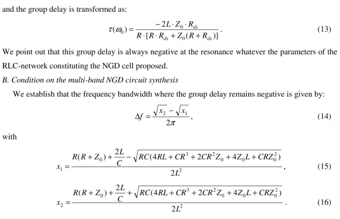
Fig. 4: RF-part of the considered dual-band NGD microwave circuit.
At noted that during the simulations, the FETs F1,2 were replaced by the complete EC2612-model
including the parasitic elements (Cgs, Cgd, Cds, Ls, Lg, Ld …) provided by Mimix BroadbandTM. By using the Momentum environment of ADS-simulator version 2008 from AgilentTM, the microstrip layout pictured in Fig. 5 was designed. This hybrid device is printed on the RF-35 substrate with
relative permittivity εr = 3.5 and thickness h = 508 µm.
input
Cdb
Vds
Vgs
Rm = 56 Ω R1 = 9.1 Ω R2 = 8.2 Ω R3 = 36 Ω
L1 = 4.3 nH
L2 = 2.2 nH
L3 = 3.6 nH C1 = 3 pF
C2 = C3 = 1 pF
FET EC2612 : F1 = F2 gm = 98.14 mS Rds = 116.8 Ω
DC blocking capacitor
Cdb= 1 µF
bias networks
Lb = 470 nH Cb = 1 µF
Substrate: RF-35, εr = 3.5
h = 508 µ m
Cdb
Cdb Cb
Cb
Lb
Lb
Lb L1
L2
L3 R1
R2
R3 Rm
C1
C2
C3
o
u
tp
u
t
F1
F2
Fig. 5: Microstrip circuit layout: RF parts in black, bias network layout in green, white circles indicate ground via-holes.
Vds= 5V and Vgs = -0.3V. Geometrical size: 13.3 mm x 13.3 mm.
B. Frequency results
We emphasize that during the simulations the passive components R, L and C are modeled by
realistic Surface Mount Components available in ADS library. After EM/circuit co-simulation, one
gets the results displayed in Fig. 6. So, we can see in Fig. 6(a) that it presents two frequency bands of
NGD. The first NGD frequency band delimited from 0.81 GHz to 1.21 GHz (NGD-bandwidth 400
MHz) presents a group delay minimal value, τ1 = –1.16 ns at the resonance frequency of about f1 =
1.05 GHz. While, the second NGD frequency band which is defined from 1.72 GHz to 2.37 GHz
(NGD-bandwidth 605 MHz) reveals a group delay minimal value equal to τ2 = –0.92 ns at f2 = 2.05
stage, but with the RLC-networks chosen, the circuit under study was optimized in order to attain the
desired NGD value. Moreover, in the operating frequency bands chosen, the positive group delay is
widely lower than the absolute value of the NGDs. As illustrated by the stability factor µ(S) given in
relation (24) below and plotted in Fig. 7, the circuit under investigation is unconditionally stable from
0.5 GHz to 2.5 GHz.
21 12 21 12 22 11 * 11 22
2 11
) (
1 )
(
S S S S S S S S
S S
+ −
−
− =
µ , (24)
where S11* =conjugate(S11) .
Frequency (GHz)
f
1f
2G
ro
u
p
d
e
la
y
(
n
s
)
|S
2
1
|
(d
B
)
(a )
2 0
dB(|S22|) dB(|S11|)
R
e
tu
rn
lo
s
s
e
s
(
d
B
)
1 5
1 0
5
0 - 1 .5 0
- 0 .7 5 0 .0 0 0 .7 5 1 .5 0
0 .5 1 .0 1 .5 2 .0 2 .5
0 -1 0 -2 0
Frequency (GHz)
(b )
0 .5 1 .0 1 .5 2 .0 2 .5
Fig. 6: Simulation results of the proposed dual-band NGD circuit.
(a) Insertion gain S21 and group delay. (b) return losses S11 and S22.
Frequency (GHz)
S
ta
b
il
it
y
f
a
c
to
r 5.0
2.5
0.0
0.5 1.0 1.5 2.0 2.5
Fig. 7: Stability factor µ(S) of the device under test.
The input and output return losses S11 and S22 displayed in Fig. 6(a) confirm this stability and the
device depends on the FET-EC2612 specifications. The harmonic balance analysis allows to affirm
that the device has P1dB of about 20 dBm.
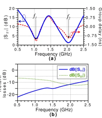
C. Time-domain results
In order to get a good insight about the dual-band NGD functionality, time-domain analyses were
also performed. For that, Gaussian signals with different standard deviations modulating microwave
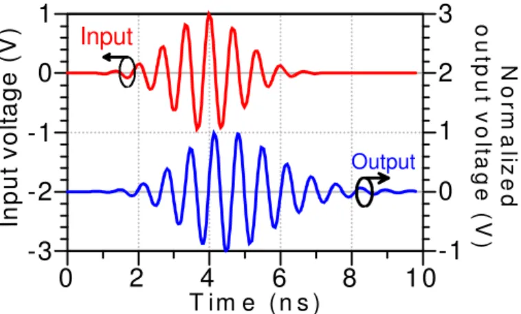
sine carriers, f1 and f2 were considered. First, regarding a Gaussian pulse input with standard deviation
ns 1.3
1=
∆T modulating f1-carrier, an output Gaussian pulse with maximal peak in advance of about
0.56 ns (or 43 % of ∆T1) is observed as plotted in Fig. 8(a).
In p ut
Output
In
p
u
t
v
o
lt
a
g
e
(
V
)
1O
u
tp
u
t v
o
lta
g
e
(V
)
T im e ( n s ) In p ut
Output
0
-1
-2
-3
0
-2 2 4 6
0 2 4 6 8
(b )
T im e (n s )
0 2 4 6 8
(a )
10
In
p
u
t
v
o
lt
a
g
e
(
V
)
10
-1
-2
-3
O
u
tp
u
t v
o
lta
g
e
(V
)
0
-2 2 4 6
Fig. 8: Time-domain responses of the considered devices shown in Fig. 4 by considering Gaussian input pulse modulating
sine carriers: (a) f1 = 1.05 GHz and (b) f2 = 2.05 GHz.
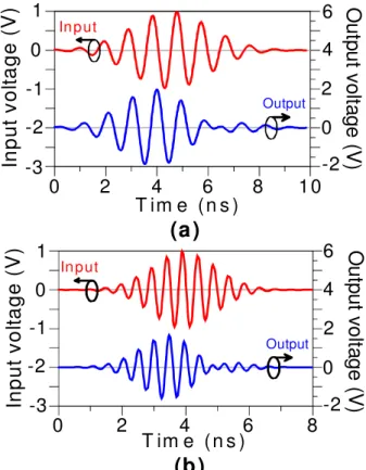
Then, by injecting Gaussian pulse input with standard deviation ∆T2 =1ns modulating f2-carrier, a time-advance of about 0.54 ns (or 54% of ∆T2) is obtained. It is interesting to notice that when injecting to the circuit under test a pulse signal with spectrum centered at fPGD = 1.5 GHz, a positive
group delay (PGD) is generated, as depicted in Fig. 9. As shown in the time-domain response, the
Input
Output
In
p
u
t
v
o
lt
a
g
e
(
V
)
N
o
rm
a
liz
e
d
o
u
tp
u
t
v
o
lt
a
g
e
(
V
)
T im e ( n s )
0
2
4
6
8
1 0
0
1
-1
-2
-3
1
0
-1
2
3
Fig. 9: Time-domain responses of the NGD devices shown in Fig. 4
by considering an input pulse with spectrum out of NGD bands (modulated at fPGD = 1.5 GHz).
These results allow to explain that this NGD effect can be useful to the signal delay compensation in
microwave frequency bands. It is noteworthy that these results are accompanied also by a
time-dependent pulse width compression as reported in [43]. But this effect does not occur for the PGD
frequency band as depicted in Fig. 9.
IV. CONCLUSION
An application of a microwave active device capable for generating a dual-band NGD and signal
amplification is investigated. It is based on the use of NGD active cells comprised of shunt series
RLC-networks in cascade with a transistor [28-30]. A synthesis methodology of the dual-band NGD
device is described.
To verify the proposed concept feasibility, S-parameter analysis of two-stage NGD hybrid device is
made with a standard microwave/electronic circuit simulator. As result, a dual-band NGD effect
having minimal value of about –1 ns was realized in the frequency bands centered at 1.05 GHz and
2.05 GHz. In order to highlight the dual-NGD device principle in more concrete aspect, time-domain
investigations were also performed. For that the implemented device was excited by Gaussian pulses
having standard deviation of about 1 ns modulating sine carriers set at the peaks of the NGD
frequency bands. As expected, pulse signals with output envelopes presenting a time-advance were
confirmed. However, it was demonstrated also that in the PGD frequency band, the output is
absolutely delayed compared to the input signal.
The transient results of dual- or multi-band NGD devices can be used for compensating signal
delays in multi-channel propagation media. Their field of applications concerns the
RF/microwave-signal delay compensation as introduced in [24-27], the correction of data synchronization in certain
RF/digital systems and the enhancement of multi-channel like MIMO modular in terms of
REFERENCES
[1] R. Mumford, “European carriers face capacity crunch challenges,” Int. Report, Microwave J., pp. 169-170, Apr. 2010. [2] S. Pal, and R. Cheung, “Two-arm archimedean spiral helical antenna with wraparound,” Microwave Journal, pp.
194-204, Apr. 2010.
[3] A. Lazaro, D. Girbau, and R. Villarino, “Effects of interferences in UHF RFID systems,” Progress In Electromagnetics Research, Vol. 98, pp. 425-443, 2009.
[4] M.A. Antoniades and G.V. Eleftheriades, “A multiband monopole antenna with an embedded reactance-cancelling transmission-line matching network,” IEEE Antennas and Wireless Propagation Letters, Vol. 9, pp. 1107-11010, 2010. [5] G. V. Eleftheriades, correction to “A generalized negative-refractive-index transmission-line (NRI-TL) metamaterial for
dual-band and quad-band applications,” IEEE Microwave and Wireless Letters, Vol. 20, No 2, pp. 130, Feb. 2010. [6] O. F. Siddiqui, A. S. Mohra and G. V. Eleftheriades, “Quad-band power divider based on left-handed transmission
lines,” IET Electronics Letters, Vol. 46, No. 21, pp. 1441-1442, 2010.
[7] L. Markley and G. V. Eleftheriades, “Quad-band negative-refractive-index transmission-line unit cell with reduced group delay,” IET Electronics Letters, Vol. 46, No 17, pp. 1206-1208, 19 Aug. 2010.
[8] G. V. Eleftheriades, “Design of generalised negative-refractive-index transmission lines for quad-band applications,” IET Microwaves, Antennas and Propagation, (Special Issue of Metamaterials), Vol. 4, No. 8, pp. 977-981, Aug. 2010. [9] C. Sabah, “Novel, dual band, single and double negative metamaterials: Nonconcentric delta loop resonators,” Progress
In Electromagnetics Research B, Vol. 25, 225-239, 2010.
[10]H. Choi, S. Shim, Y. Jeong, J. Lim, C. D. Kim, S.-Y. Eom, and Y.-B. Jung, “2.14/3.5 GHz novel dual-band negative group delay circuit design based on composite right/left handed transmission line,” In Proc. of 2010 European Microwave Conference (EuMC), Paris, France, 28-30 Sep. 2010, pp. 441-444.
[11]H. Choi, Y. Jeong, J. Lim, S.-Y. Eom, and Y.-B. Jung, “A novel design for a dual-band negative group delay circuit,” IEEE Microwave and Wireless Letters, Vol. 21, No. 1, pp. 19-21, Jan. 2011.
[12]K. Y. Cheung, S. Y. Zheng, W. S. Chan, and K. F. Man, “Dual-band hybrid coupler with extended bandwidth,” Microwave and Optical Technology Letters, Vol. 52, No. 9, pp. 2095-2098, Sep. 2010.
[13]K. M. Dani, Z. Ku, P. C. Upadhya, R. P. Prasankumar, A. J. Taylor, and S. R. J. Brueck, “Ultrafast nonlinear optical spectroscopy of a dual-band negative index metamaterial all-optical switching device,” Optics Express, Vol. 19, No. 5, pp. 3973-3983, 2011. doi:10.1364/OE.19.003973
[14]Z. Abate, “WiMAX RF systems engineering,” Mobile communication series, Artech House 2009, Norwood, MA, USA. [15]S.-S. Myoung, B.-S. Kwon, Y.-H. Kim and J.-G. Yook, “Effect of group delay in RF BPF on impulse radio systems,”
IEICE Tran. Communications, Vol. 90, No. 12, pp. 3514-3522, 2007.
[16]C. D. Broomfield, and J .K. A. Everard, “Broadband negative group delay networks for compensation of oscillators, filters and communication systems,” Electron. Lett., Vol. 23, pp. 1931-1933, Nov. 2000.
[17]H., Noto, K., Yamauchi, M., Nakayama, and Y. Isota, “Negative group delay circuit for feed-forward amplifier,” IEEE Int. Microw. Symp. Dig., pp. 1103-1106, Jun. 2007.
[18]K.-P. Ahn, R. Ishikawa, and K. Honjo, “Group delay equalized UWB InGaP/GaAs HBT MMIC amplifier using negative group delay circuits,” IEEE Tran. MTT, Vol. 57, No. 9, pp. 2139- 2147, Sep. 2009.
[19]B. Ravelo, M. Le Roy, and A. Perennec, “Application of negative group delay active circuits to the design of broadband and constant phase shifters,” Microwave and Optical Technology Letters, Vol. 50, No. 12, pp. 3077-3080, Dec. 2008. [20]B. Ravelo, A. Perennec and M. Le Roy, “Study and application of microwave active circuits with negative group
delay,” Microwave and Millimeter Wave Technologies Modern UWB Antennas and Equipment, Chap. 21, INTECH Book, Ed. By I. Minin, pp. 415-439, Mar. 2010.
[21]S. Keser, and M. Mojahedi, “Broadband negative group delay microstrip phase shifter design,” in Proc. of IEEE Ant. Prop. Soc. Int. Symp. 2009 (APSURSI’09), 1-5 June 2009.
[22]B. Ravelo, A. Perennec and M. Le Roy, “Broadband balun using active negative group delay circuit,” in Proc. of 37th EuMC, Munich, Germany, pp. 466-469, Oct. 2007.
[23]K.-P. Ahn, R. Ishikawa, and K. Honjo, “UWB active balun design with small group delay variation and improved return loss,” IEICE Trans. on Electronics, 2011, Vol. 94, No. 5, pp. 905-908.
[24]B. Ravelo, A. Perennec and M. Le Roy, “Experimental validation of the RC-interconnect effect equalization with negative group delay active circuit in planar hybrid technology”, in Proc. of 13th IEEE Workshop SPI, Strasbourg, France, May 2009.
[25]B. Ravelo, A. Perennec and M. Le Roy, “New technique of inter-chip interconnect effects equalization with negative group delay active circuits,” VLSI, Chap. 20, INTECH Book, Ed. by Z. Wang, pp. 409-434, Feb. 2010.
[26]S. K. Podilchak, B. M. Frank, A. P. Freundorfer, and Y. M. M. Antar, “High speed metamaterial-inspired negative group delay circuits in CMOS for delay equalization,” in Proc. of 2nd Microsystems and Nanoelectronics Research Conference 2009 (MNRC 2009), pp. 9-12, 13-14 Oct. 2009.
[27]Y. Osaki, T. Hirose, K. Matsumoto, N. Kuroki, and M. Numa, “Delay-compensation techniques for ultra-low-power subthreshold CMOS digital LSIs,” in Proc. of 52nd IEEE Int. Midwest Symp. CAS 2009 (MWSCAS'09), 2-5 Aug. 2009, pp. 503-506.
[28]B. Ravelo, A. Perennec, M. Le Roy, and Y. Boucher, “Active microwave circuit with negative group delay,” IEEE MWC Lett., Vol. 17, No. 12, pp. 861-863, Dec. 2007.
[29]B. Ravelo, A. Perennec, and M. Le Roy, “Synthesis of broadband negative group delay active circuits,” in Proc. of IEEE MTT-Symposium IMS 2007, Honolulu, Hawaii, USA, pp. 2177-2180, 3-8 June 2007.
[31]B. Ravelo, “Baseband NGD circuit with RF amplifier,” Electronic Letters, Vol. 47, No. 13, 23rd June 2011, pp. 752-754.
[32]L. Brillouin, and A. Sommerfeld, “Wave propagation and group velocity,” Academic Press, New York, 1960, pp. 113-137.
[33]A. Dogariu, A. Kuzmich, H. Cao, and L. J. Wang, “Superluminal light pulse propagation via rephasing in a transparent anomalously dispersive medium,” Optics Express, Vol. 8, No. 6, pp. 344-350, Mar. 2001.
[34]G. V. Eleftheriades, O. Siddiqui, and A. K. Iyer, “Transmission line for negative index media and associated implementations without excess resonators,” IEEE Microwave and Wireless Letters, Vol. 13, No. 2, pp. 51-53, Feb. 2003.
[35]O. F. Siddiqui, M. Mojahedi, and G. V. Eleftheriades, “Periodically loaded transmission line with effective negative refractive index and negative group velocity,” IEEE Trans. Ant. Prop., Vol. 51, No. 10, Oct. 2003, pp. 2619-2625. [36]O. F. Siddiqui, S. J. Erickson, G. V. Eleftheriades, and M. Mojahedi, “Time-domain measurement of negative-index
transmission-line metamaterials,” IEEE Trans. MTT, Vol. 52, No. 5, May 2004, pp. 1449-1453.
[37]C. D. Broomfield, and J. K. A. Everard, “Broadband negative group delay networks for compensation of oscillators using feedforward amplifiers,” Electronics Letters, Vol. 20, pp. 1710-1711, Sep. 2000.
[38]M. Kitano, T. Nakanishi, and K. Sugiyama, “Negative group delay and superluminal propagation: An electronic circuit approach,” IEEE J. Selected Topics in Quantum Electronics, Vol. 9, No. 1, pp. 43-51, 2003.
[39]N. S. Bukhman, and S. V. Bukhman, “On the Negative Delay Time of a Narrow-Band Signal as It Passes through the Resonant Filter of Absorption,” Radiophysics and Quantum Electronics, Vol. 47, No. 1, 2004, pp. 66-76.
[40]M. W. Mitchell, and R. Y. Chiao, “Negative group delay and ‘fronts’ in a causal systems: An experiment with very low frequency bandpass amplifiers,” Phys. Lett. A, Vol. 230, pp. 133-138, Jun. 1997.
[41]M. W. Mitchell, and R. Y. Chiao, “Causality and negative group delays in a simple bandpass amplifier,” Am. J. Phys., Vol. 66, pp. 14–19, 1998.