Brazilian Microwave and Optoelectronics Society-SBMO received 1 June, 2010; revised 7 Oct., 2010; revised 10 Jan., 2011; accepted 18 Jan., 2011 Brazilian Society of Electromagnetism-SBMag © 2011 SBMO/SBMag ISSN 2179-1074
Study on Effect of Rectangular DMS and
DGS on 4 and 8 Elements Rectangular
Microstrip Linear Array Antenna
S L Mallikarjun, P M Hadalgi and P V Hunagund
Microwave Laboratory, Dept. of PG Studies and Research in Applied Electronics, Gulbarga University, Gulbarga – 585 106, Karnataka (INDIA).
Abstract - In this experimental study a novel design has been
developed to improve the antenna parameters in terms of impedance bandwidth and radiation properties. A 4-element rectangular array antenna (refereed as antenna 1) operating in the range of 10 to 16 GHz with multi bands is used as a reference antenna. The impedance bandwidth and other radiation properties have been enhanced by using defected microstrip structure (DMS) and defected ground structure (DGS). This study is further extended to 8-element array. The design consideration and experimental results of the proposed antennas are presented and discussed.
Index Terms – DMS, DGS, impedance bandwidth, radiation properties
I. INTRODUCTION
Microstrip patch antennas are the new generation of the antennas due to their low profile,
inexpensive to manufacture and easy to integrate with monolithic microwave integrating circuit
(MMICs) design [1]. However the main disadvantage of the microstrip patch antenna is their narrow
impedance bandwidth and excitation of the surface wave. The input impedance of the antenna tends to
be sensitive to change in frequency; hence the deviation of the antenna input impedance from a real
fixed value often determines the operating range of the antenna. The input impedance of the antenna
depends on its geometrical shape, dimension and feed type. Therefore, the antenna input impedance is
a very important design parameter, which controls the radiating power and impedance bandwidth.
In certain applications, such as high data-rate wireless transmission, this low bandwidth is not
adequate. In order to meet the demand for large bandwidth, several techniques have been reported, the
most commonly employed technique is increasing the thickness of the substrate supporting the
microstrip patch. However limitations still exist on the ability to effectively feed the patch on a thick
substrate and the radiation efficiency can degrade with increasing substrate thickness [2]. Techniques
for overcoming this band limiting problem can be achieved using the parasitic tuning elements,
Brazilian Microwave and Optoelectronics Society-SBMO received 1 June, 2010; revised 7 Oct., 2010; revised 10 Jan., 2011; accepted 18 Jan., 2011 Brazilian Society of Electromagnetism-SBMag © 2011 SBMO/SBMag ISSN 2179-1074
Impedance bandwidth and radiation properties of microstrip antenna (MSA) are also enhanced by
using DMS and DGS. Defected ground structure was first proposed by Park et.al., based on the idea
of photonic band-gap (PBG) structure, and had found its application in the design of planar circuits
and low pass filters [3]. DGS and DMS is realized by etching a specific pattern in the ground plane of
the microstrip structure(DGS) or on the microstrip surface (DMS), DGS disturbs the shield current
distribution in the ground plane. This disturbance can change the characteristic of a transmission line
such as equivalent capacitance and inductance to obtain the slow-wave effect and band-stop property
[4]. Due to insertion of DGS/DMS there is an additional inductance occurs due to the magnetic flux
flow in the etched out aperture and gap capacitance on ground plane. Surface impedance is changed
due to an etched defect which in turn disturbs the shield current distribution in the plane. The change
in surface impedance changes its phase velocity of the current. The change in phase velocity leads in
change in the apparent effective permittivity.
Many shapes of DGS slot have been studied for single element microstrip antenna such as circle,
dumbbells and spiral. Recently for 2 element array a hexagonal DGS is studied [5], however not many
have realized it in antenna arrays.
In this experimental study, a novel design has been developed by using DMS and DGS. A
4-element rectangular microstrip array antenna (antenna 1) operating in the range of 10 to 16 GHz
resonating for multi bands has been used as a reference antenna. It has been observed from the
detailed study that by using DMS and DGS impedance bandwidth and other radiation properties are
improved. Further the study is extended to 8-element rectangular microstrip array antenna.
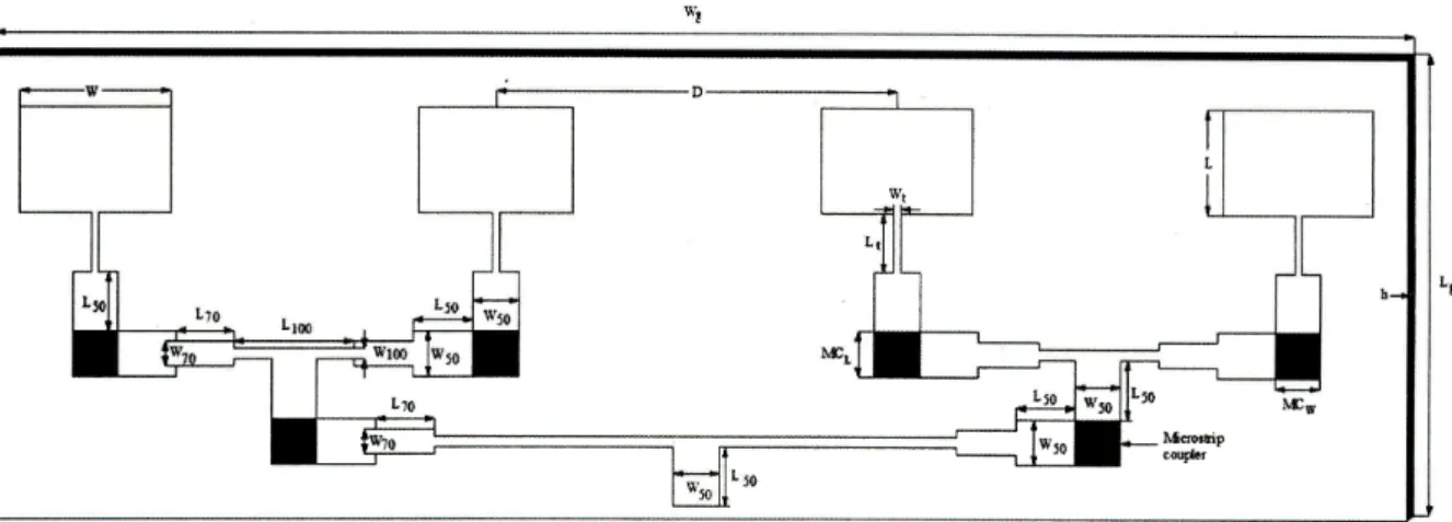
II. ANTENNA CONFIGURATION
The proposed antennas are designed using low cost glass epoxy material having dielectric constant
Єr = 4.2, thickness h = 0.166 cm and loss tangent tan δ = 0.02. The geometry of antenna 1 is shown in
Fig. 1.
Brazilian Microwave and Optoelectronics Society-SBMO received 1 June, 2010; revised 7 Oct., 2010; revised 10 Jan., 2011; accepted 18 Jan., 2011 Brazilian Society of Electromagnetism-SBMag © 2011 SBMO/SBMag ISSN 2179-1074
The elements of array are designed for 9.4 GHz frequency with dimensions L and W. The length Lg
and Wgof the ground plane of antenna is calculated using Lg = 6h + L and Wg = 6h + W [6]. The
elements of this array antenna are excited through simple corporate feed arrangement. This feed
arrangement consists of matching transformer, quarter wave transformer, microstrip coupler and
power divider for better impedance matching between feed and radiating elements [7]. A two-way
power divider made up of 70Ω matching transformer of dimension (L70, W70) is used between 100Ω
microstrip line of dimension (L100, W100) and 50Ω microstrip line of dimension (L50, W50). A
microstrip coupler of dimension (MCL, MCW) is used between 50Ω microstrip lines to couple the
power [8], [9]. The 50Ω microstrip line is connected at the center of the driven element through a
quarter wave transformer of dimension (Lt, Wt) for better impedance matching. At the tip of microstrip
line feed of 50Ω, a coaxial SMA connector is used for feeding the microwave power. The array
elements are kept at a distance of D = 5λ0/6 from their center point, where λ0 is the free space
wavelength in centimeters. This optimized distance is selected in order to achieve minimum side lobes
in the radiation pattern and to add the radiated power in free space. The various dimensions mentioned
in Fig. 1, Fig. 2 and Fig. 3 are given in table I.
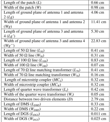
TABLE I – DIMENSIONS OF PATCH, CORPORATE FEED LINE NETWORK, DMS and DGS
Length of the patch (L) 0.66 cm
Width of the patch (W) 0.98 cm
Length of ground plane of antenna 1 and antenna 2 (Lg)
4.06 cm
Width of ground plane of antenna 1 and antenna 2 (Wg)
11.41 cm
Length of ground plane of antenna 3 and antenna 4 (Lg’)
5.30 cm
Width of ground plane of antenna 3 and antenna 4 (Wg’’)
22.83 cm
Length of 50 line (L50) 0.41 cm
Width of 50 line (W50) 0.31 cm
Length of 100 line (L100) 0.83 cm
Width of 100 line (W100) 0.07 cm
Length of 70 line matching transformer (L70) 0.41 cm
Width of 70 line matching transformer (W70) 0.16 cm
Length of microstrip coupler (MCL) 0.32 cm Width of microstrip coupler (MCW) 0.32 cm Length of quarter wave transformer (Lt) 0.42 cm Width of the quarter wave transformer (Wt) 0.05 cm Distance between two driven elements (D) 2.79 cm
Length of DMS (LDMS) 0.33 cm
Width of DMS (WDMS) 0.22 cm
Length of DGS (LDGS) 0.011 cm
Width of DGS (WDGS) 0.025 cm
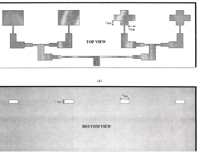
Fig. 2 shows the process of building the new DMS and DGS shaped array antenna (referred as
antenna 2). To increase the impedance bandwidth of antenna 1, the last two elements of array are
modified by inserting four rectangular DMS with same dimensions LDMSand WDMS as given in table I,
Brazilian Microwave and Optoelectronics Society-SBMO received 1 June, 2010; revised 7 Oct., 2010; revised 10 Jan., 2011; accepted 18 Jan., 2011 Brazilian Society of Electromagnetism-SBMag © 2011 SBMO/SBMag ISSN 2179-1074 rectangular DGS of dimension LDGS and WDGS as given in table I is used exactly below all the four
elements [11].
(a)
(b)
Fig. 2. Geometry of antenna 2 (a) Top view, (b) Bottom view
Brazilian Microwave and Optoelectronics Society-SBMO received 1 June, 2010; revised 7 Oct., 2010; revised 10 Jan., 2011; accepted 18 Jan., 2011 Brazilian Society of Electromagnetism-SBMag © 2011 SBMO/SBMag ISSN 2179-1074
Fig. 4. Geometry of antenna 4
The study is extended for 8-element rectangular microstrip array antenna with DMS and DGS as
shown in Fig. 3 (referred as antenna 3). Further, Fig. 4 shows the geometry of 8-element rectangular
microstrip array antenna with all the radiating elements modified by inserting DMS and DGS
(referred as antenna 4). Fig. 5 shows the photo of all the proposed antennas.
(a)
(b)
Brazilian Microwave and Optoelectronics Society-SBMO received 1 June, 2010; revised 7 Oct., 2010; revised 10 Jan., 2011; accepted 18 Jan., 2011 Brazilian Society of Electromagnetism-SBMag © 2011 SBMO/SBMag ISSN 2179-1074
III. EXPERIMENTAL RESULTS AND DISCUSSION
The impedance bandwidths for the proposed antennas are measured at 4 to 18 GHz frequencies.
The measurements are taken on Vector Network Analyzer (Rohde & Schwarz, German make ZVK
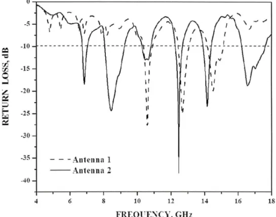
Model No. 1127.8651). The variation of return loss versus frequency of antenna 1 and antenna 2 are
shown in Fig. 6. The variation of return loss versus frequency of antenna 3 and antenna 4 are shown
in Fig. 7.
From Fig. 6, it is observed that the antenna 1 is resonating for three bands at 10.63 GHz, 12.74 GHz
and 14.63 GHz with magnitude 600 MHz (5.64 %), 630 MHz (4.94 %) and 910 MHz (6.21 %). From
the figure it is clear that the antenna 2 is resonating for six bands at 6.87 GHz, 8.44 GHz, 10.47 GHz,
12.47 GHz, 14.15 GHz and 16.56 GHz with magnitude 280 MHz (4.05 %), 1160 MHz (13.38 %), 520
MHz (4.92 %), 420 MHz (3.36 %), 490 MHz (3.46 %) and 1440 MHz (8.50 %). This increase in the
number of bands is due to inserting DMS and DGS, the impedance bandwidth of the antenna is also
improving and antenna is resonating at lower frequencies causing increase in bands with improved
bandwidth.
Fig. 6. Variation of Return loss V/S Frequency of antenna 1 and antenna 2
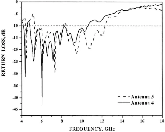
From Fig. 7, it is observe that the antenna 3 is resonating for three bands at 4.49 GHz, 7.32 GHz
and 9.49 GHz with magnitude 210 MHz (4.68 %), 2840 MHz (42.32 %) and 3920 MHz (37.80 %).
This shows that, by increasing the elements of antenna 2 i.e., from 4 to 8, the performance of the
Brazilian Microwave and Optoelectronics Society-SBMO received 1 June, 2010; revised 7 Oct., 2010; revised 10 Jan., 2011; accepted 18 Jan., 2011 Brazilian Society of Electromagnetism-SBMag © 2011 SBMO/SBMag ISSN 2179-1074 5.29 to 8.13 GHz and 8.41 to 12.33 GHz. It is clear from the graph that, the proposed antenna 3 is
covering almost C-band and X-band. Further, from the graph it is observed that the antenna 4 is
resonating for two bands at 4.35 GHz and 6.03 GHz with magnitude 420 MHz (9.65 %) and 5810
MHz (75.4 %). This shows that, inserting DMS and DGS on all 8 elements of the array will result into
a small band in the range 4.14 to 4.56 GHz and a wide band covering from 4.80 to 10.61 GHz. Hence,
it is observed that by inserting DMS and DGS, the impedance bandwidth of the array antenna is
improved and the antenna resonates for lower frequency when compared to antenna 1. The minimum
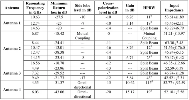
return loss of all the proposed antennas measured at resonating frequencies is tabulated in table II.
Fig. 7. Variation of Return loss V/S Frequency of antenna 3 and antenna 4
The far-field H - plane co-polar and cross-polar radiation patterns of all the proposed antennas are
measured at their resonating frequencies. In this study the turn-table method is used to measure the
radiation pattern of all the proposed antennas (AUT). Here AUT is kept in the receiving mode and the
reference antenna (Pyramidal Horn) is kept in transmitting mode. The two antennas are placed so as to
face each other and then, keeping the position of transmitting antenna fixed, the receiving antenna is
rotated around axis, by changing the angle in steps of degrees. At each angle the received power is
measured. The graph is plotted for azimuth angle versus normalized power.
Fig.8 to Fig. 10 show the radiation patterns of antenna 1, Fig.11 to Fig. 16 show the radiation
patterns of antenna 2 and Fig. 17 to Fig. 19 show the radiation patterns of Antenna 3. These figures
Brazilian Microwave and Optoelectronics Society-SBMO received 1 June, 2010; revised 7 Oct., 2010; revised 10 Jan., 2011; accepted 18 Jan., 2011 Brazilian Society of Electromagnetism-SBMag © 2011 SBMO/SBMag ISSN 2179-1074 seen that by inserting DMS and DGS on all the 8 elements of the array, the radiation characteristic of
the antenna is improved as unidirectional pattern of the antenna is converted to omni-directional. The
side lobe levels and cross polarization levels of all the antennas at the resonating frequencies are
measured and are mentioned in table II. At some frequencies, the proposed antennas show split beam
radiation patterns which are useful in SAR for generating a pair of forward and backward squinted
beams and provide simultaneous measurement of both the along-track and the cross-track velocities
[12]. The half-power beamwidths (HPBWs) of all the proposed antennas are calculated for their
resonating frequencies and are tabulated in table II for comparison. The gains of all the proposed
antennas are measured at the resonating frequencies using gain comparison method [1] and are also
tabulated in table II.
Fig. 8 Fig. 9
Fig. 10 Fig. 11
Brazilian Microwave and Optoelectronics Society-SBMO received 1 June, 2010; revised 7 Oct., 2010; revised 10 Jan., 2011; accepted 18 Jan., 2011 Brazilian Society of Electromagnetism-SBMag © 2011 SBMO/SBMag ISSN 2179-1074
Fig. 14 Fig. 15
Fig. 16 Fig. 17
Fig. 18 Fig. 19
Brazilian Microwave and Optoelectronics Society-SBMO received 1 June, 2010; revised 7 Oct., 2010; revised 10 Jan., 2011; accepted 18 Jan., 2011 Brazilian Society of Electromagnetism-SBMag © 2011 SBMO/SBMag ISSN 2179-1074
Fig. 20 Fig. 21
TABLE II — MEASURED RETURN LOSS, SIDE LOBE LEVEL, CROSS-POLAR LEVEL, GAIN AND CALCULATED HPBW WITH RESPECT TO RESONATING FREQUENCIES
Antenna Resonating Frequency in GHz Minimum Return loss in dB
Side lobe level in dB
Cross-polarization
level in dB
Gain
in dB HPBW
Input Impedance
Antenna 1
10.63 -27.5 -10 -10 6.26 110 53.61+j1.89
12.74 -25 -7 -10 3.14 180 45.45+j2.11
14.63 -20 --- -14 --- Split Beam 43.22+j6.79
Antenna 2
6.87 -18.42 Mutual
Coupling
-5 --- Mutual
Coupling
51.21- j13.97
8.44 -24.41 --- -11 --- Split Beam 63.30-j3.48
10.47 -13.01 --- -16 8.76 120 51.56+j176.0
12.47 -38.38 --- -14 Split Beam 46.84+j5.15
14.15 -23.41 -8 -10 6.74 230 50.47+j1.42
16.56 -18.78 --- -12 --- Split Beam 46.35- j12.66
Antenna 3
4.49 -23.96 ---- -13 --- Split Beam 52.59-j6.39
7.32 -29.52 ---- -7 --- Split Beam 46.74- j1.28
9.49 -21.73 -17 -12 5.84 430 42.52+ j2.31
Antenna 4
4.35 -31.37
Omni-directional
-15 10.62 1150 52.77+ j92.59
6.03 -43.06
Omni-directional
-20 15.17 190 52.18+ j2.58
IV CONCLUSION
A new design has been developed using DMS and DGS. The rectangle shape DMS and DGS have
been used for 4 and 8 element rectangular microstrip antenna array. The results demonstrate that
impedance bandwidth and radiation properties of the antennas are improved by increasing the array
elements with DMS and DGS. These antennas are more superior as these are fabricated using low cost
substrate material. These antennas are more suitable for modern communication systems and in radar
systems like SAR for tracking the target as soon as finding them and for anti-jamming.
ACKNOWLEDGMENT
We thank the authorities of Department of Science and Technology (DST), Govt, of India, New
Delhi, for sanctioning Vector Network Analyzer under the FIST Programme to the Department of
Applied Electronics, Gulbarga University, Gulbarga.
REFERENCE
[1] C. A. Balanis, “Antenna theory, analysis and design”, John Wiley and Sons. Inc., New York, 1982.
[2] D. M. Pozar, “Microstrip antennas”, IEEE Proc. Antenna Propag., vol. 80, pp. 79-81, 1992.
[3] Kim, C. S., J. I. Park, A. Dal, et. al., “A novel 1-D periodic defected ground structure for planer circuits”, IEEE Microwave Guided Wave Lett., vol. 10, no. 4, pp. 131-133, 2000.
[4] A. K. Shrivastav, Promad Kumar, Jugal Kishor, Rashid Mahmood, “Impedance BW enhancement technique in microstrip circuits by using DGS and DMS”, Int. Symp. on Microwave and Optical Tech. New Delhi, pp. 532-535, 2009.
Brazilian Microwave and Optoelectronics Society-SBMO received 1 June, 2010; revised 7 Oct., 2010; revised 10 Jan., 2011; accepted 18 Jan., 2011 Brazilian Society of Electromagnetism-SBMag © 2011 SBMO/SBMag ISSN 2179-1074
[6] Bahl I J and Bharatia P, “Microstrip Antennas”, Artech House, New Delhi, 1981.
[7] Kai Fong Lee & Weichen, “Advances in Microstrip and Printed Antennas”, John Wiley, New York, 1997.
[8] Jeong Kim I I and Young Joong Yoon, “Design of wideband microstrip array antennas using the coupled lines,” IEEE Antenna and Prop. Soci. Int. Symp., vol. 3, pp. 1410-1413, 2000.
[9] Oing X M and Chin Y W M, “Circularly polarized circular ring slot antenna fed by stripline hybrid coupler,” Electron Lett., vol. 35, no. 25, pp. 2145-2155, 1999.
[10] S. L. Mallikarjun, R. G. Madhuri, S. A. Malipatil and P. M. Hadalgi, Compact high gain multi frequency antenna,
IEEE-Int. Symp. on Microwaves 2008, Bangalore, IND,pp. 369-373, 2008.
[11] S. L. Mallikarjun, R. G. Madhuri and P. M. Hadalgi, “Effect of rectangular DGS on rectangular microstrip patch array antenna”, Int. Symp. on Microwave and Optical Tech. New Delhi, pp. 257-260, 2009.
[12] John Huang and Soren N. Madsen, “A dual beam microstrip array antenna”, IEEE Antenna and Prop. Soci. Int. Symp., Chicago, vol. 1, pp. 147-150, 1992.