*e-mail: [email protected]
Recebido: 10/03/2013 / Aceito: 09/07/2013
Electromagnetic interference reduction by dynamic impedance
balancing applied to biosensors
João Francisco Ribeiro Negrão*, Guilherme Augusto Limeira Araujo, Carlos Tavares da Costa Júnior, Daniel Cardoso de Souza
Abstract Introduction:Electromagnetic interference caused by electric power lines adversely affects the signals of electronic instruments, especially those with low amplitude levels. This type of interference is known as common-mode interference. There are many methods and architectures used to minimize the inluence of this kind of interference on electronic instruments, the most common of which is the use of band-reject ilters. This paper presents the analysis, development, prototype and test of a new reconigurable ilter architecture for biomedical instruments, aiming to reduce the common-mode interference and preserve the useful signal components in the same frequency range as that of the noise, using the technique of dynamic impedance balancing. Methods:The circuit blocks were mathematically modeled and the overall closed-loop transfer function was derived. Then the project was described and simulated in the VHDL_AMS language and also in an electronics simulation software, using discrete component blocks, with and without feedback. After theoretical analysis and simulation results, a prototype circuit was built and tested using as input a signal obtained from ECG electrodes. Results:The results from the experimental circuit matched those from simulation: a 97.6% noise reduction was obtained in simulations using a sinusoidal signal, and an 86.66% reduction was achieved using ECG electrodes in experimental tests. In both cases, the useful signal was preserved. Conclusion:The method and its architecture can be applied to attenuate interferences which occur in the same frequency band as that of the useful signal components, while preserving these signals. Keywords Biomedical instruments, Electromagnetic interference, Common-Mode Rejection,
are unbalanced, the gain and the CMRR of the signal processing circuit will be strongly degraded. These deleterious effects can be reduced using both electronic and mechanical techniques, such as increasing the CMRR of the signal processing circuit (Degen and Jackel, 2008; Grimbergen etal., 1996; Spinelli etal., 2004, 2006), or shielding the data cables by an external metal mesh.
The loss of signal strength due to the unbalance in electrode wires or input terminals tends to increase as distance grows between the transducers or sensors and the input circuits. Some techniques, such as the Instrumentation Ampliier (IA) architecture (Dobrev and Daskalov 2009), can reduce the common-mode interference (Vcm) range about 200 times, when applied to an electrocardiogram signal (Berbari, 2000) (Figure 1). Some authors like Degen (Degen and Jackel, 2008) proposed to reduce the unbalance, caused by sensor disconnection of the patient’s skin, by monitoring a reference voltage generated by a “driven-right-leg circuit (DRL)”, while Spinelli
architecture. This circuit presents reconigurable characteristics and could be easily used in any noise range by reprogramming the microprocessor which controls the band pass ilters (BPF). The prototype circuit design is based on the reconigurability concept (Negrão etal., 2006). A model described in VHDL-AMS (Mentor Graphics, 2006) allows us to validate the basic principles of operation, and the software “Isis Proteus Schematic Capture” (Labcenter Electronics, 1989-2009) is used for the design of a test version with discrete components. The experimental results validate those obtained in simulation.
Theoretical Foundation
The architecture proposed in this paper aims to attenuate Vcm by reducing the amount of impedance unbalance. However, when compared to other methods (Degen and Jackel 2008; Grimbergen etal., 1996; Spinelli etal., 2004, 2006), the approach presented here has the advantage of attenuating only Vcm, with small impact on the useful signal components (Vd), even if they are in the same frequency range as the noise.
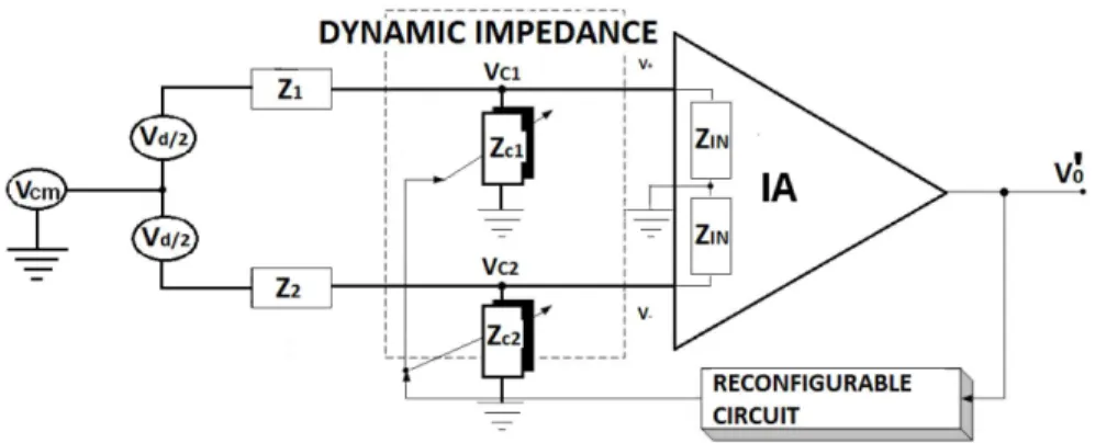
The unbalance of the electrodes’ input impedances is dynamically compensated for by a counter circuit in a feedback system (the RECONFIGURABLE CIRCUIT), which controls a bank of impedances as shown in Figure 2. The structure and operation of the circuit are described below.
Where:
Vcm = common-mode interference (noise) signal; Vd/2 = biopotential signal at each electrode; V+ and V- = voltages at the IA input;
Z1 and Z2 = impedances of the input electrodes; Zc1 and Zc2 = dynamically-adjustable impedances; Zin = IA input impedance;
RECONFIGURABLE CIRCUIT = circuit responsible for dynamically controlling the adjustable impedances;
V0 = adjusted output signal.
The impedance unbalance reduction is viable by means of a feedback loop (RECONFIGURABLE CIRCUIT) which, depending on the variation of the maximum amplitude of the output signal (V0′), readjusts
the values of the input impedances (ZC1 and ZC2) to yield an output signal with minimal interference. These values are achieved when the impedance balancing condition of Equation 1 (Dobrev and Daskalov, 2009) is satisied, meaning that the common-mode noise was canceled.
Zc1 + Z1 = Zc2 + Z2 (1)
The general equation of a non-feedback ampliier is only governed by its internal components, and it is shown in Equation 2, where Acm is the common-mode gain of the ampliier, and Ad is the
differential-mode gain of the ampliier. Equation 3 deines the transfer function of our architecture (Figure 2), using the principle of feedback by reconigurability (Negrão et al., 2006). Equation 3 is composed of three terms, but since our main analysis goal in this work is the noise component Vcm, and not Vd or the CMRR, only the second term of Equation 3 will be taken into consideration. This yields a revised
0′
V (Equation 4), which is directly inluenced by
the balancing of the cable impedances (Z1, Z2, and ZC1, ZC2), the noise (Vcm) and the Ad at the IA inputs. The new V0′ in equation 4 will be used in
the rest of this paper. Equation 5 is used to measure the level of unbalance determined by the new proposed architecture. This is the same method used to determine the level of unbalance in longitudinal telephone cables (Volpato and Magalhães, 2009). After appropriate values (ZC1 = 2.5 MΩ, ZC2 = 10 kΩ, Z1 = Z2 = 1.2 MΩ) are replaced in Equation 6,
the worst-case unbalance value predicted for the architecture is BAL = –0.6674 dB.
0′ = d⋅ d+ cm⋅ cm
V V A V A (2)
( ) ( ) ( ) ( ) ( ) ( ) ( ) ( ) ( ) ( ) ( ) ( ) 1
1 1 1
0
2
2 2 2
1
1 1 1
2
2 2 2
2 2 2 2 2 + ⋅ ⋅ − + + ⋅ ′ = ⋅ ⋅ + + ⋅ ⋅ + + ⋅ + ⋅ ⋅ − + + ⋅ + ⋅ ⋅ + + ⋅ d
cm c in
c in c in d
d d
cm c in
c in c in
d
cm c in
c in c in
d
cm c in
c in c in
V
V Z Z
Z Z Z Z Z V
V A
V
V Z Z
Z Z Z Z Z
V
V Z Z
Z Z Z Z Z
V
V Z Z
Z Z Z Z Z
⋅ ⋅ + ⋅ d
cm d cm
A
V A V
CMRR (3)
(
)
(
) (
)
(
)
(
) (
)
11 1 1
0
2
2 2 2
2 2 + ⋅ ⋅ − + + ⋅ ′ = ⋅ ⋅ + ⋅ ⋅ + + ⋅ d
cm c in
c in c in
cm d d
cm c in
c in c in
V
V Z Z
Z Z Z Z Z
V V A
V
V Z Z
Z Z Z Z Z
(4)
2 1
20 log − ( )
= ⋅ C C
cm V V BAL dB V (5)
(
)
(
) (
)
(
)
(
) (
)
22 2 2
1
1 1 1
2
2
20 log ( )
+ ⋅ ⋅ − + + ⋅ + ⋅ ⋅ + + ⋅ = ⋅ d
cm c in
c in c in
d
cm c in
c in c in
cm
V
V Z Z
Z Z Z Z Z
V
V Z Z
Z Z Z Z Z
BAL dB
V
(6)
Where Vd =Vd/2+Vcm.
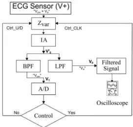
of 2.55 MΩ. This is possible with the use of analog switches, each controlled by a four-bit counter. As the signal amplitude is low, it needs to be ampliied, and that is done by the IA. A sample of the signal after iltering by the 2nd-order LPF (VO) is sent to be
analyzed later with an oscilloscope. Another sample of the signal, after being iltered by a 4th-order BPF (V1) with 30 Hz bandwidth (which allows only the EMI components between 40 and 70 Hz to pass), passes through the A/D converter implemented in the PIC16F877 microcontroller (with an 8-bit data bus, 4 MHz clock, 2400 bps processing capacity, and a 19.53 mV resolution).
This is what distinguishes this prototype from those submitted in earlier works (Dobrev and Daskalov, 2002; Negrão etal., 2006; Spnelli etal., 2004): the analysis of noise (Vcm), separated from the useful signal (Vd).
After the signal is sampled and processed with 8 bits of deinition, there are 255 discrete voltage values (decimal values), which means that each level in the ladder conversion is 19.53 mV, for a 5 V reference voltage. As the signal at the IA output (INA 122) (V0′ as observed in the algorithm of Figure 3) is at a
but if the noise level of the sample is beyond the amplitude reference range, then it is considered that the dynamic impedance circuit is unbalanced. In this case, a high level (5V) is sent to turn on the clock of the counter circuit (Ctrl_U/D), and another high level prompting positive increment of the counter (UP), increasing the equivalent impedance of the block (Zvar). As the sampling process happens every 1 millisecond, the system is dynamically fed back by the most recent sample and if this sample indicates that the Vcm amplitude still increased even outside the reference range (even after 3 clock cycles, or 3 ms), the system considers that the action of counting up is incorrect, and then a low level (zero volts) is sent to the loop counter for decrementing the dynamic impedance (DW), to ind again a balance of Zvar. When balance is found, the clock counter circuit is switched off again and waits for instructions to turn the system on again in order to conserve battery power. However, it is observed that the electromagnetic noise amplitude changes constantly and the system stays on continuously.
Variable impedance block
The variable impedance block consists of a group of resistances (Zc), which is described by equation 7.
2
( 1)
1 2 −
= ⋅ ∑NB NB C
Z R (7)
Where:
R is the irst resistance value;
NB is the number of bits used in the A/D converter. The circuit is completed with analog switches and counters, as detailed in Table 1.
Instrumentation ampliier block (IA)
Besides the implementation of an IA, a high-pass ilter (HPF) was added to minimize the noise below 0.3 Hz (Equation 8), while the IA gain (GIA) is given by equation 9.
( )2
( ) 1
ω ⋅ ⋅ =
+ ω ⋅ ⋅ C R H S
C R (8)
200 5 = + IA G K G R (9) Where:
RG is the gain resistance, located inside the IA block (Figure 7 and Table 1);
ω is angular velocity.
The gain is kept at low levels in the IA (GIA ≈ 14 dB) to avoid saturating the ilter blocks.
Low-pass and band-bass ilters block
The filters design was based on the RAUCH architecture, in which the multiple feedback (MFB) topology is characterized by high gains and quality factor (Q), and its general transfer function is shown in Equation 10.
3 1 1 1 3 1 3
5 5 4 2 5 4 5
1 − = ⋅ ⋅ + + + + ⋅ ⋅ out in Z
Z R R R R R R R
R R R R R R R
(10)
From this standard block, after the appropriate resistance and capacitance values are replaced, other ilters can be quantiied: a 2nd-order LPF
and its corresponding transfer function shown in equations (11, 12, 13 and 14), and a BPF composed of two cascaded 2nd-order blocks, each one described
by equations (15, 16, 17 and 18), equivalent to a 4th-order ilter. All the ilter parameters have been
calculated to yield a 3 dB attenuation. In the output of the BPF block, the signal intentionally received a higher gain as compared to other blocks.
0
2 2
1 1 0
( ) =
+ + ω
LPF
a H S
b S a S (11)
2 0
1 = −R
a
R (12)
2 3
1 0 1 2 3
1
⋅
= ω ⋅ ⋅ + +
R R
a C R R
R (13)
2
1= ω ⋅ ⋅0 1 2⋅ 2⋅ 3
b C C R R (14)
1
2 2
_ 2º
1 2 0
( ) = ⋅
+ + ω
BPF
a S H S
b S b S (15)
2 3
1 0
1 3
⋅
= − ⋅ ⋅ ω +
R R
a C
R R (16)
2 2 3 2 3
1 0
1 3
⋅ ⋅
= ⋅ ⋅ ω
+
R R R
b C
R R (17)
1 3
2 0
1 3
2
⋅ ⋅
= ⋅ ⋅ ω
+
R R
b C
R R (18)
Where:
ω0 is the fundamental angular velocity.
Control block
The control block is formed by the PIC microcontroller (Table 1, Figure 7) and a DC level shifter circuit to keep a 2.5 V reference. A better description of the control block is given above, on the “Circuit modeling” section.
Transfer functions
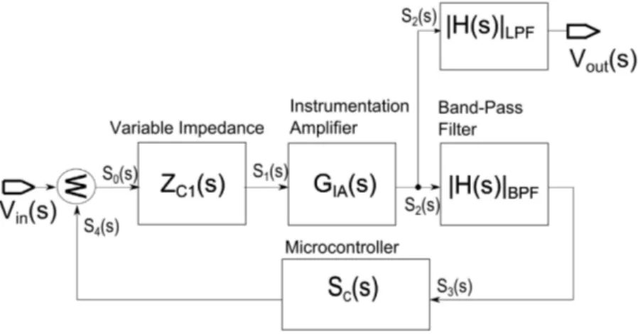
As all the main sub-circuits have been mathematically presented, the overall closed-loop transfer function (Equation 24) is shown in Figure 4.
The transfer function (Equation 24) could be used to analyze how all the sub-circuits in the system affect the output signal. For instance, taking as reference the control signal (Sc(s)) which represents the processing and control system block, if this signal is not properly
Table 1. List of components and description.
Component Quant. Speciication Description
V A R I M P
Resistor (Ω) 12 10k, 20k, 40k, 80k, 160k, 320k,
640k, 1280k, 2.55M, 2x100k. Carbon resistor.
Analog Switch 8 HEF4016 (Philips Semiconductors) Analog switch.
Counter 2 CD4029 (Philips Semiconductors) Digital counter.
IA
IA 1 INA122 (Burn-Brown) Instrumentation ampliier.
RG (Ω) (Pins 1 and 8 of the
INA122) 1 200K Variable resistor (trimpot).
F I L
Filter LPF (2nd order) 1 OP 07 (Texas Instruments) Active Filter - 4 kHz. Filter BPF (4th order) 2 OP 07 (Texas Instruments) Active ilter - 60 Hz. C
O N
AND gate 1 74LS00 (Philips Semiconductors) Digital circuit.
processed, it can lead all other sub-circuits to an uncontrolled state.
Where:
0( )= in( )− 4( )
S s V s S s (19)
(
)
1( )= in( )− 4( ) ⋅ C1( )
S s V s S s Z s (20)
(
)
2( )= IA( )⋅ C1( )⋅ in( )− 4( )
S s G s Z s V s S s (21)
(
)
3( )= IA( )⋅ C1( )⋅ ( )BPF in( )− 4( )
S s G s Z s H s V s S s (22)
1 4
1
( ) ( ) ( ) ( ) ( )
( )
1 ( ) ( ) ( ) ( )
⋅ ⋅ ⋅ ⋅
=
+ ⋅ ⋅ ⋅
IA C BPF C in
IA C C BPF
G s Z s H s S s V s
S s
G s Z s S s H s (23)
1
1
( ) ( ) ( )
( )
( ) 1 ( ) ( ) ( ) ( )
⋅ ⋅
= =
+ ⋅ ⋅ ⋅
IA C
out LPF
in IA C C BPF
G s Z s H s
V s
FT
V s G s Z s S s H s (24)
Design and Simulation
Design and simulation using description in VHDL_AMS
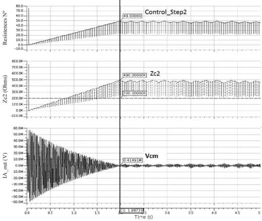
Initially, the project was described in the VHDL_AMS language and simulated in the Mentor Graphics ADVANCE platform (Mentor Graphics, 2006). For the input stimuli, only the common-mode signal (Vcm) was considered, with frequency fcm and Offset = 0. It means that, in the analysis of simulation results (Figure 5), the useful signal (Vd1 and Vd2) will not be present and only the interference (Vcm) will be displayed.
The results of two simulations in VHDL_AMS, given a constant Zin1 and a varying Zin2, are shown in Figure 5, where three curves are displayed: the irst one represents the amplitude control (Control_Step2), in number of resistors (Resistance No); the second one represents the increment or decrement in the resistor bank (ZC2), or the equivalent impedance in
ohms, and the third one represents the interference signal (Vcm), in volts (V).
In Figure 5, Vcm is attenuated and maintained at the lowest level of amplitude possible, by means of the closed loop control which leads to the impedance balancing (Equation 1).
Design and simulation using discrete components
The design and simulations were also performed using the Proteus software “ISIS Professional v7.0” (Labcenter Electronics, 1989-2009). The project was divided as shown in Table 1 in which the electronic components used in the prototype are detailed.
Where:
VAR IMP = variable impedance block; IA = instrumentation ampliier block; FIL = ilters block;
CON = control block.
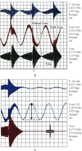
Since it wasn’t possible to obtain typical digitized pre-stored ECG signals, an equivalent sinusoidal signal was used as a test vector for the simulations, with the same amplitude and frequency characteristics of an ECG signal, besides being strongly inluenced by EMI. Figures 6a, b present the simulation results obtained from the circuit designed in the PROTEUS software when characteristic signals obtained from biosensors are applied in order to reduce common-mode noise (Vcm).
In Figure 6a, three graphs are shown representing the simulation results of the noise reduction system without feedback or control, upon application of a typical bioelectric signal in the input. The irst graph represents the total signal (in the common and differential modes), after ampliication by the constant-gain IA (V_IA-Out), the second graph represents the biosignal at the output of the LPF (Vcm + Vd), and
the third graph represents the noise at the output of the BPF (Vcm). In this case, the system has no feedback and the interference amplitude ranges approximately between a maximum value (Vcm_Max ≈ 1.19 Vp) and a minimum value (Vcm_Min ≈ 34.0 mVp). Vd also suffers interference from Vcm, such that the useful signal becomes hidden (Vcm >> Vd). This begins to change as the impedance matching occurs at the IA input, due to the common-mode signal feedback, causing a progressive loss of Vcm range, without affecting the Vd amplitude. Thus, the useful signal becomes more visible (Vcm << Vd).
After feedback is implemented in the circuit, the system simulation yields the graphs in Figure 6b. The top graph represents the output of the IA (V_IA-Out); the second graph is the output of the LPF ilter; and the third graph is the output of the BPF ilter.
Results
Prototype circuit
After theoretical analysis and simulation results, a prototype circuit was constructed (Figure 7) where the LPF and BPF ilters were implemented in PSOC CY8C27443 microcontrollers.
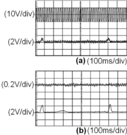
The prototype tests were performed using as input a signal obtained from ECG electrodes (2223BRQ-3M type, one electrode on each wrist and a third one on the left leg of the patient). Resulting data are shown in Figures 8a, b. In Figure 8a, the circuit has no feedback, i.e., no control. In this case, Vcm completely overwhelms the ECG signal (Vd). However, in Figure 8b, the circuit has feedback and the ECG signal is more visible in comparison to the noise. Both Figures 8a, b were obtained inside the electromagnetic noise band (60Hz).
Analyzing the oscillation of the signal in Figure 8b, it is observed that its period is approximately 0.3 seconds, which means a frequency around 3 Hz. Actually, the total oscillation period of the signal shown in the oscilloscope screen (before the signal was highlighted) is approximately 0.018 seconds, which means a frequency around 55.25 Hz. Figure 8b was presented that way only to highlight the achieved results, without modifying or corrupting the obtained data.
Discussion
The main aspects that distinguish this work from Silva’s work (Silva, 2003) are the control of the impedance bank and its voltage-divider geometry. In
Finally, Silva’s work (Silva, 2003) did not produce a physical prototype which could validate his own simulation results. This paper goes beyond simulations and produces a prototype which conirms the results obtained and the modiications proposed.
Analysis of the results obtained shows that the proposed prototype circuit achieved its primary goal, which was reducing the common-mode interference (Vcm) while preserving the useful components of the signals to which the system was conceived (Vd1 and Vd2), as shown in Figures 5, 6b and 8b. As for the graph representing Vcm, from the analysis of Figure 6, we ind that the noise amplitude decreased from 1275 mVpp to 15 mVpp, meaning a percentage attenuation of 98.8%, or –38.59 dB, while the useful signal is preserved.
Figure 5 shows simulation results from the irst prototype, which was described using Mentor Graphics’ VHDL_AMS platform. This simulation shows the effects of the real-time control of the impedance balancing, from top to bottom: the balancing of the
Figure 8. Results obtained with ECG electrodes, (a) circuit without feedback and (b) with feedback.
Figure 7. Manufactured prototype in printed circuit board.
resistances of the resistor bank “Resistance Nº”, the equivalent impedance of one of the IA inputs “Zc2”, and Vcm at the IA output “IA_out”. The simulated system took around 2 seconds to reach equilibrium, that is, to reduce the input noise, which initially had a 120 mVpp amplitude, to a 0.41 mV value, after feedback was applied to the circuit. This Figure is only concerned with noise analysis. With the present prototype (Figure 7), proper responses were reached in half the time.
Analysis of the results in Figure 8, obtained from the experimental circuit, shows that the results match those obtained from simulation, where a 97.6% reduction was obtained using the sinusoidal signal (or Vcm = –32.39 dB), and a 86.66% reduction was achieved using ECG electrodes (or Vcm = –17.50 dB), Figures 8a, b.
This paper addressed the reduction of common-mode noise, specially the one originating from electromagnetic sources. We introduced the impedance balancing concept and proposed a modiied architecture for Vcm noise reduction, using dynamic input impedance balancing (ZVAR). A circuit was designed and simulated in VHDL_AMS, and also designed and simulated in discrete circuit form, employing close-to-real parameter values of discrete components found in the market, and at the end, a prototype circuit was built and tested.
Excellent results were obtained, validating the proposed architecture and its application to signals that need to be controlled without the use of complex circuits or ilters, many of which will override both the noise signals (in common-mode), but also the components of the useful signal (in differential mode).
Acknowledgments
The authors would like to thank the ALBAN program and FADESPA for their technical and inancial support.
References
Berbari EJ. Principles of electrocardiography. In: The Biomedical Engineering Handbook: Second Edition. Boca Raton: CRC Press; 2000.
Degen T, Jackel H. Continuous monitoring of electrode–skin impedance mismatch during bioelectric recordings. IEEE
Transactions on Biomedical Engineering. 2008; 55:711-5. http://dx.doi.org/10.1109/TBME.2008.919118
Dobrev D, Daskalov L. Two-electrode biopotential ampliier with current-driven inputs. Medical & Biological Engineering & Computing. 2002; 40:122-7. http://dx.doi.org/10.1007/ BF02347705
Grimbergen CA, VanRijin ACM, Peper A. A method for the measurement of individual electrode-skin interfaces and the implications of the electrode properties for preampliier desing. In: Annual International Conference of the IEEE Engineering in Medicine and Biology Society: Proceedings of the 14th Annual International Conference of the IEEE Engineering in Medicine and Biology Society; 1996; Paris. Paris: IEEE; 1996. v. 6, p. 2382-3.
Labcenter Electronics. Isis Proteus. 1989-2009. Available from: http://www.labcenter.co.uk/.
Mentor Graphics. Getting started with advanced MS software. Mentor Graphics; 2006. version 4.4_1 Release. AMS Tutorial.
Negrão JFR, Naviner JF, Silva IS. Circuit mixte d’interface reconigurable pour applications en instrumentation médicale. In: JNRDM 2006: Journées Nationales du Réseau Doctoral de Microélectronique; 2006; Paris, France. Paris: DonNTU; 2006. French.
Silva IS. Circuits mixtes reconigurables appliqués à la mesure de signaux biomédicaux: réjection de l’interférence de mode commun [Thesis]. Paris: Télécom Paris; 2003. French. Spinelli EM, Martinez MN, Mayosky MA, Pallas-Areny R. A novel fully differential biopotential ampiier with dc suppression. IEEE Transactions on Biomedical Engineering. 2004; 51(8):1444-8. http://dx.doi.org/10.1109/ TBME.2004.827931
Spinelli EM, Mayosky MA, Pallas-Areny R. A practical approach to electrode-skin impedance unbalance measurement. IEEE Transactions on Biomedical Engineering. 2006; 53(7):1451-3. http://dx.doi.org/10.1109/ TBME.2006.875714
Yamamoto AY, Nakamura T, Kitaoka K. Automatic interference controller device for eliminating the power-line interference in biopotential signals. In: IMTC 2000: Proceedings of the 17th IEEE Instrumentation end Measurements Technology Conference; 2000; Baltimore. Baltimore: IEEE; 2000. v. 3, p. 1358-62.
Volpato RM, Magalhães GVB. Método para a medição de balanceamento longitudinal em terminais telefônicos. In: SEMETRO: Anais do 8ºSeminário Internacional de Metrologia Elétrica; 2009; Campina Grande, Brazil. Campina Grande: Universidade Federal de Campina Grande; 2009. Portuguese.
Authors
João Francisco Ribeiro Negrão*
Instituto de Tecnologia – ITEC, Universidade Federal do Pará – UFPA, Rua Augusto Corrêa, 01, Guamá, CEP 66075-110, CP 479, Belém, PA, Brasil.
Guilherme Augusto Limeira Araujo, Carlos Tavares da Costa Júnior, Daniel Cardoso de Souza