J. Nano- Electron. Phys.
3 (2011) No1, P. 601-609 (Sumy State University) 2011 SumDU
601
PACS numbers: 61.72.Uj, 78.20.Ci, 78.30.FS, 78.55.Et
LASER INDUCED NONLINEAR OPTICAL PROPERTIES OF ZINC OXIDE THIN FILM PREPARED BY SOL-GEL METHOD
Vinay Kumari1, Vinod Kumar2, B.P. Malik3, Devendra Mohan4, R.M. Mehra5
1 Department of Physics, BMIET,
131 001, Sonepat, India
E-mail: [email protected]
2 Department of Physics, Gurukula Kangri University,
249 404, Haridwar, India E-mail: [email protected]
3 Department of Physics, DCRUST,
131 027, Murthal, India
E-mail: [email protected]
4 Department of Physics, GJU&ST,
125 001, Hissar, India E-mail: [email protected]
5 School of Engineering and Technology, Sharda University,
201 306, Greater Noida, U.P., India E-mail: [email protected]
Optical nonlinearities of spin coated ZnO thin film have been investigated by using single beam Z-Scan technique in the visible region. X- ray diffraction shows that all films are oriented along the c-axis direction of the hexagonal crystal structure. The average optical transmittance of all films is higher than 80 %. The nonlinear optical parameters viz. nonlinear absorption coefficient (), nonlinear index of refraction (2),
nonlinear susceptibility (3), have been estimated using nanosecond laser pulses of
second harmonic of Nd:YAG Laser. The value of nonlinear absorption coefficient is estimated to be greater than the already reported value. The films clearly exhibit a ve value of nonlinear refraction at 532 nm which is attributed to the two photon absorption and free carrier absorption. The presence of RSA in ZnO thin films inferes that ZnO is a potential material for the development of optical limiter.
Keywords: ZnO, NONLINEAR ABSORPTION, NONLINEAR INDEX OF REFRACTION, OPTICAL LIMITING, NONLINEAR SUSCEPTIBILITY, Z-SCAN. (Received 04 February 2011, in final form 18 June 2011)
1. INTRODUCTION
ZnO thin films have attracted much attention because of its versatile nature. It is less expensive, n-type direct band gap semiconductor with Eg value of
602 VINAY KUMARI, VINOD KUMAR, B.P. MALIK, ET AL.
found that ZnO has a strong nonlinear second order susceptibility 2, which
results in second harmonic generation [4, 5].
Nanostructures of ZnO are fabricated using various thin film techniques as spray pyrolysis [6], molecular beam epitaxy [7], chemical vapor deposition (CVD) [8], vacuum evaporation [9], pulsed laser deposition [10], RF Sputtering [11] and sol-gel processing [12, 13]. All these processes are associated with complicated methodologies except sol-gel. Sol-gel allows us to fabricate large area coating at relatively low cost. It controls the microstructure of the films and the optical and electrical properties can be tailored easily by adding suitable dopant.
During the present course of investigation, we have estimated the nonlinear optical properties of ZnO thin films deposited on corning (1737) glass substrate by sol. gel method using spin coating technique. The films have been characterized by a single beam Z-scan technique under illumination of Nd:YAG laser at 532 nm.
2. EXPERIMENTAL DETAIL
In order to obtain good quality ZnO thin film from sol-gel technique, the precursor sols for the films were prepared from zinc acetate dihydrate [(Zn (CH3COO)2 2H2O), purity 99.95 %], methanol and monoethanolamine
(MEA). The solution was stirred magnetically for about 120 minutes to obtain clear and homogeneous solution and was kept for aging for 48 hours before the deposition of the films [14]. Corning glass (1737) slides were used as substrate for spin coating of the film. These glass substrates were cleaned ultrasonically by acetone, methanol and deionised water for 15 minutes and at last were dried in nitrogen atmosphere. The spinning speed and time were optimized to 2500 rpm and 30 seconds respectively, so that each spun layer is thin enough for evaporation of all solvents and thus preventing the films from cracking. The films were then dried in air at 300 C for 10 min. The spin coating process was repeated fifteen times in order to get a film thickness of ~ 300 nm. The finally deposited films were annealed at optimized temperature of 450 C for 1 hour [15]. The structural properties of the annealed film were investigated by X-ray diffractometer (Rigaku Corporation) using CuK radiations.
LASER INDUCED NONLINEAR OPTICAL PROPERTIES OF… 603
the aperture was removed (S 1) completely. The radius of the beam waist 0 was calculated to be 24.3 µm. The Rayleigh length (z0) was found to
satisfy the criterion of a Z-scan experiment. The obtained data was analyzed by the procedure described by the pioneer worker Sheik Bahae et al. [16].
Fig.1 Shematic representation of a single beam Z-scan experiment setup: lens (L); focal point of lens (Z); Sample (S); Aperture (A); Detector (D); Oscilloscope (O)
3. RESULTS
3.1 Structural properties
The structural properties of the film were investigated by X-ray diffraction studies. The X-ray 2 scan pattern of ZnO thin films deposited on a glass substrate at an annealing temperature of 450C are shown in Fig. 2. One can clearly observe a diffraction peak at ~ 34.47C corresponding to the (002) plane of ZnO exhibiting the hexagonal wurtzite structure
corresponding to the preferential c-axis orientation in the film due to lowest surface free energy of this plane.
Fig.2 XRD pattern of ZnO thin film 2 (deg.)
In
te
n
si
ty
(
a.
u
604 VINAY KUMARI, VINOD KUMAR, B.P. MALIK, ET AL.
3.2 Surface Morphology
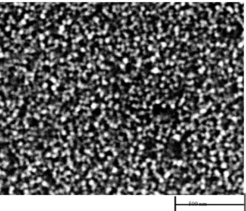
Surface morphology of ZnO thin films were investigated by scanning electron microscopy. SEM micrograph of ZnO film is shown in Fig. 3 with presence of tightly packed grains. All films show smooth surface with a fine structure without cracks and voids. The grain size of ZnO is observed approximately 16 nm.
500 nm
Fig. 3 – SEM image of ZnO thin films annealed at 450 C
3.3 Optical Properties
Transmittance measurements were carried out in the range 200-800 nm to estimate the band gap of the films and are shown in Fig. 4. The average transmission within the visible wavelength region for all the films was higher then 80 %. The firings in transmittance spectra show that ZnO films have good homogeneity.
Fig.4 Optical Transmittance spectra of ZnO films
In the direct transition semiconductor, the absorption coefficient, obeys the following relationship with optical energy band gap (Eg) [17]:
Wavelength (nm)
T
ra
n
sm
it
ta
n
ce
LASER INDUCED NONLINEAR OPTICAL PROPERTIES OF… 605
h(h Eg)1/2
where h is Planck’s constant and is the frequency of incident photon. So the band gap of ZnO film is estimated by plotting graph of h vs (h)2 for
the linear absorption coefficient . Extrapolation of the linear part until it intersects the h axis gives us the value of band gap (Eg).The value optical
band gap (Eg) is found to be shifted from that of the bulk as shown in
Fig. 5. The total change in the band gap of the material is simultaneously contributed by shifts of the valence and the conduction band edges with respect to each other [18]. Generally the shift of the top of the valance band (TVB) is not the same as that of the bottom of the conduction band (BCB). A larger shift for the BCB is expected in view of the fact that the band edge shifts are related inversely to the corresponding effective masses of electron and hole. The effective mass of the electron is always much smaller than that of the hole in these II-VI semiconductors [19].
Fig.5 Plot of (h)2 on (h) of ZnO films
Photoluminescence spectrum of ZnO films are shown in Fig. 6 exhibiting emission peak at 385 nm.This peak lie in UV region and corresponds to band to band transition [20].
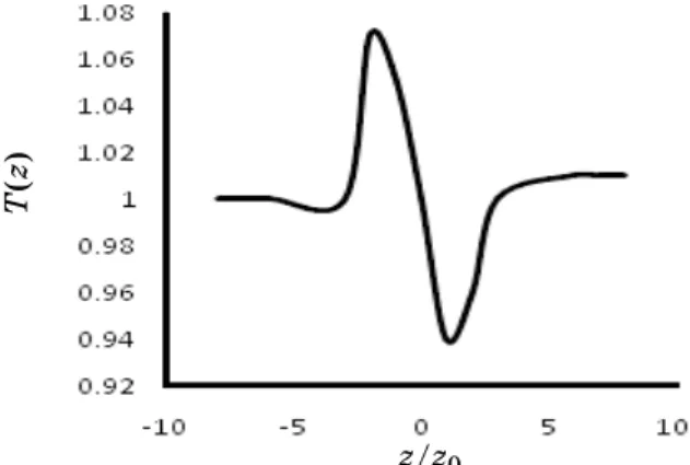
Typical results of the open aperture Z-scan measurements of the film that corresponds to the far-field normalized tranmittance, T (z) as a function of the distance from the lens focus at an intensity of 2.1 TW/cm2 are shown in
Fig. 7. The open aperture curve exhibits a normalized transmitted valley, indicating the presence of reverse saturable absorption (RSA) in the films. In the presence of RSA, transmittance T (z) of the films is calculated as:
0 2 2
0
1 ,
2 2 1 q T z
z z
(1)
where q0 I0Leff, I0 is the irradiance of laser beam at focus, Leff is the
h (eV)
(
h
)
2 (
cm
-1eV
)
606 VINAY KUMARI, VINOD KUMAR, B.P. MALIK, ET AL.
Fig.6 Photoluminescence spectrum of ZnO films
Fig.7 Open aperture Z-scan measurements
effective thickness of the sample, which is defined as:
e
,Leff L
1 (2)
where L is the real thickness.
From Fig. 7 the value of q0 is obtained to get the value of. The value of
, gives us directly the value of imaginary part of susceptibility (Im(3))through the relation:
3 0 02
Im ,
4
(3)
where, is the excitation wavelength, n0 is the linear refractive index of
ZnO, 0 is the permittivity of free space and c the velocity of light in
vacuum.
In
te
n
si
ty
(a
.u
.)
Wavelength ()
z/z0
N
or
m
al
iz
ed
T
ra
n
sm
it
ta
n
ce
T
(z
LASER INDUCED NONLINEAR OPTICAL PROPERTIES OF… 607
In general, induced absorption can occur due to a verity of processes. The theory of two photon absorption (TPA) process fitted well with the experimental curve and two photons of 532 nm radiation lie below the absorption band-edge of the samples under investigation infers that TPA is the basic mechanism. There is possibility of higher order nonlinear processes such as free carrier absorption (FCA) contributing to induced absorption. It is already reported that carrier lifetime of ZnO is 2.8 s [21] plot as we are using 5 ns pulses to excite the free carriers generated by TPA so we can say that TPA and FCA are the two important mechanism responsible for RSA in our sol-gel thin films. RSA is also responsible for optical limiting effects, so the sample can also be used as an optical limiter.
Fig. 8 Normalised transmittance with closed-aperture as a function of the position The closed aperture Z-scan plot is shown in Fig. 8 at an intensity of 2.1 TW/cm2 .The graph clearly exhibits the presence of a peak followed by a
valley, which indicates a ve value of coefficient of nonlinear refraction 2
and can be estimated as:
0
2 2 0,25
0 . 40 0,812 1
p v
eff
T c
esu
S I L
(4)
The value of Tp-v is the difference between peak and valley transmittance
and it can be determined by the best theoretical fit from the Z-scan curve. The value of 2 is associated with the real part of nonlinear susceptibility Re (3)
as:
3
0 2
Re .
3 esu esu
(5)
The absolute value of (3) can be obtained by using formula:
(3)(esu) { [Im(3)]2 + [Re(3)]2 }1/2. (6)
The value of nonlinear absorption coefficient is estimated to be greater than the already reported values because of good crystalinity of the film free from any voids shown our XRD and SEM data. The results are in good agreement as that of reported by various research workers. It is observed
T
(
z
)
608 VINAY KUMARI, VINOD KUMAR, B.P. MALIK, ET AL.
Table 1 Measured values of absorption coefficient, nonlinear refractive index, real and imaginary Parts of third order nonlinear susceptibility (3)and total
value of (3)of ZnO films at I
02.1 TW/cm2 and wavelength of 532 nm
Sample
Nonlinear absorption coefficient ()
(cm/W)
Nonlinear refractive index
(2)
(cm2/W)
Img. (3)
(esu) Real
(3)
(esu)
(3)
(esu)
ZnO Thin film
sample 1.46 10
– 6 – 1.54 10 – 10 3.149 10 – 5 – 1.57 10 – 4 2.5 10 – 4
that the real part of (3) is larger than the imaginary part of (3) that implies
stronger refraction effect. By comparing the work done by various researchers we found that the nonlinear absorption coefficient () values are quiet high indicating that ZnO thin film sample has good nonlinear response and are therefore potential candidate for Optoelectronic devices.
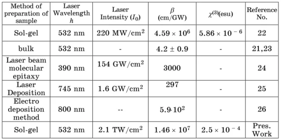
Table 2 Comparison of work done about the values of and (3) for ZnO
samples measured by Z-Scan technique Method of
preparation of sample
Laser Wavelength
h
Laser Intensity (I0)
(cm/GW) (3)(esu) Reference No.
Sol-gel 532 nm 220 MW/cm2 4.59106 5.8610 – 6 22
bulk 532 nm - 4.2 0.9 - 21,23
Laser beam molecular
epitaxy 390 nm
154 GW/cm2
3000 - 24
Laser
Deposition 745 nm 1.6 GW/cm2 297 - 25
Electro deposition
method 800 nm -- 5.910
2 - 26
Sol-gel 532 nm 2.1 TW/cm2 1.46107 2.510 – 4 Pres.
Work 4. CONCLUSIONS
The nonlinear optical properties of ZnO thin film developed by spin coating sol-gel technique have been investigated. The sample exhibits a negative nonlinear index of refraction at 532 nm and the observed nonlinear refraction is attributed to two photon absorption. The real part of (3) is found to be
larger than the imaginary part. Further the RSA behavior implies that ZnO is a good candidate for optical limiting.
LASER INDUCED NONLINEAR OPTICAL PROPERTIES OF… 609
REFERENCES
1. S.A. Studenikin, N. Golego, M. Cocivera, J. Appl. Phys.84, 2287 (1998). 2. D.C. Look, Mater. Sci. Eng. B80, 383 (2001).
3. Z.K. Tang, G.K.L. Wong, P. Yu, M. Kawasaki, A. Ohtomo, H. Koinuma, Y. Segawa, Appl. Phys. Lett. 72, 3270 (1998).
4. H. Cao, J.Y. Wu, H.C. Ong, J.Y. Dai, R.P.H. Change, Appl. Phys. Lett. 73, 572
(1998).
5. U. Newmann, R. Grunwald, U. Griedner, G. Steinmeyer, Appl. Phys. Lett. 84, 170
(2004).
6. P. Nunes, E. Fortunato, R. Martins, Int. J. Inorg. Matter.3, 1125 (2001). 7. H. Yoshikawa, S. Adachi, Jap. J. Appl. Phys.36, 6237 (1997).
8. Y. Kashiwaba, F. Katahira, K. Haga, T. Sekiguchi, H. Watanabe, J. Cryst. Growth
221, 431 (2000).
9. A. Aly, N.Z.Al. Sayed, M.A. Kaid, Vaccum61, 1 (2001).
10.X.W. Sun, R.F. Xaio, H.S. Kwok, J. Appl. Phys.84, 5776 (1998). 11.V. Gupta, A. Mansingh, J. Appl. Phys. 80, 1063 (1996).
12.Y. Natsume, H. Sakata, Thin Solid Films372, 30 (2000). 13.W. Tang, D.C. Cameron, Thin Solid Films238, 83 (1994).
14.P. Sagar, P.K. Shishodia, R.M. Mehra, Appl. Surf. Sci. 253, 5419 (2007). 15.Ravinder Kaur, A.V. Singh, R.M. Mehra, phys. status solidi A202, 1053 (2005). 16.M. Sheik-Bahae, A.A. Said, T.H. Wei, D.J. Hagan, E.W. van Stryland, IEEE J.
Quantum Electron. 26, 760 (1990).
17.R. Kumar, N. Khare, V. Kumar, G.L. Bhalla, Appl. Surf. Sci.254, 6509 (2008). 18.Sameer Sapra, D.D. Sarma, Phys. Rev. B69, 125304 (2004).
19.L.E. Brus, J. Chem. Phys.80, 4403 (1984).
20.A. Bougrine, M. Addou, A. El Hichou, A. Kachouane, J. Ebothe, M. Lamrani, L. Dghoughi, Physical and Chemistry News 13, 36 (2003).
21.X.J. Zhang, W. Ji, S.H. Tang, J. Opt. Soc. Am. B14, 1951 (1997).
22.Litty Irimpan, A. Deepthy, Bindu Krishnan, L.M. Kukreja, V.P.N. Nampoori, P. Radhakrishnan, Opt. Comm.281, 2938 (2008).
23.X. Zhang, H. Fang, S. Tang, W. Ji, Appl. Phys. B65, 549 (1997).
24.Yun Pie Chan, Ja-Hon Lin, Chih-Chang Hsu, Wen-Feng Hsieh, Opt. Express16, 19900 (2008).
25.Ja-Hon Lin, Yin-Jen Chen, Hung-Yu Lin,Wen-Feng Hsieh, J. Appl. Phys. 97, 033526 (2005).