JOURNAL OF NANO- AND ELECTRONIC PHYSICS Р А А - А Р
Vol. 7 No 4, 04026(4pp) (2015) Том7№ 4, 04026(4cc) (2015)
2077-6772/2015/7(4)04026(4) 04026-1 2015 Sumy State University
Design Considerations of Structural Parameters in Resonant Tunneling Diode by None-Equilibrium Green Function Method
M. Charmi*, M.H. Yousefi
Department of Nano Physics, Malekashtar University of Technology, Shahinshahr, Isfahan, Iran
(Received 29 September 2015; published online 10 December 2015)
This paper presents the effects of structural parameters like Quantum well width, barrier width, spac-er width, contact width and contact doping, on pspac-erformance of Resonant Tunneling Diode using full quan-tum simulation. The simulation is based on a self-consistent solution of the Poisson equation and Schrodinger equation with open boundary conditions, within the non-equilibrium Green’s function forma l-ism. The effects of varying the structural parameters is investigated in terms of the output current, peak current, valley current, peak to valley current ratio and the voltage associated with the peak current. Sim-ulation results illustrate that the device performance can be improved by proper selection of the structural parameters.
Keywords: RTD, NEGF, Peak to valley current ratio, Peak current, Structural parameters.
PACS numbers: 73.23.Ad, 73.61.Ey, 73.40.Gk
1. INTRODUCTION
A typical GaAs / AlGaAs resonant tunneling struc-ture or diode is a 2 terminal heterostrucstruc-ture device formed by sandwiching the narrow bandgap GaAs layer between two wide bandgap AlGaAs layers. The wide band gap layers act as potential barriers for electrons in the conduction band. Resonant tunneling diodes (RTDs) present interesting characteristics. Its I-V characteristic presents an unusual negative differential resistance (NDR). Such negative differential resistance is usually achieved by a circuit involving more devices, and significant power consumption [1-2]. These RTD specificities are exploited in digital applications such as memory application [3] and analog to digital converter [4-5] as well as analog applications such as frequency divider [6], frequency multiplier [7] and oscillator [8], leading to simpler circuits reducing the size of circuit with a large gain in power consumption and high fre-quency performance. Also resonant tunneling diodes have been considered as one of the candidates for THz oscillators at room temperature [9-11].
Small electron effective masse and low band-offset in III-V heterostructures, make these materials inter-esting candidates for RTD fabrication. The first RTD with room-temperature NDR has been built with a GaAs well between two AlxGa1 – xAs barriers and GaAs emitter and collector regions structure in 1985 [12]. Among the III-V based RTDs the GaAs / AlGaAs sys-tems remain one of the best option, due to the experi-enced gained on the fabrication of this technology. Therefore the RTD layer structure of GaAs / AlGaAs RTD was studied in this article with quantum transport numerical model. The effect of the quantum well width, barrier width, spacer width, contact width and contact doping are investigated. The simulations have been done by self-consistently solving of the Pois-son equation and the Schrodinger equation with open boundary conditions, within the nonequilibrium Green’s function (NEGF) formalism.
2. DEVICE STRUCTURE AND SIMULATION
APPROACH
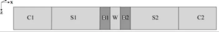
The schematic layer structure of the RTD employed in this project is shown in Fig. 1. It is noted that the un-doped gallium arsenide (GaAs) is sandwiched be-tween two thin un-doped aluminum gallium arsenide (AlGaAs) layer. Because of the difference of these two semiconductor material bandgaps, a double barrier quantum well (DBQW) is formed. An un-doped GaAs quantum well with width of 2 nm; two un-doped Al-GaAs barriers with width of 2 nm; two un-doped Al-GaAs spacer layer with width of 15 nm near by the barrier and two high dopant GaAs contacts (1E18 Cm – 3) with width of 15 nm that are connect to the two large reser-voirs. All of the values of structure parameters of our nominal device (Fig. 1) are given in Table 1.
Fig. 2– Schematic cross-sectional view of RTD, C1: Contact1,
C2: Contact2, S1: Spacer1, S2: Spacer2, B1: Barrier1, B2: Barrier2, W: Well
Table 1– Parameters for the resonant tunneling diode
struc-ture used in simulation
Device parameters Value
Quantum well width (nm) 2
Quantum barrier width (nm) 2
Spacer width (nm) 15
Contacts width (nm) 15
Contacts doping concentration (Cm– 3) 1E18
M. CHARMI,M.H. YOUSEFI J.NANO-ELECTRON.PHYS. 7, 04026 (2015)
04026-2 region and the doped contacts to prevent diffusion of impurity atoms into the barriers and well.
Since transport happens in one direction, within effective mass formulism, the device could be represent-ed by a one dimensional chain of nodes with spatially varying effective mass at material interface and period-ic boundary condition to other two directions (Fig. 1). In transport direction (the x-direction), the Non-Equilibrium Green’s Function approach which is equi v-alent to solving the Schrödinger equation with the open boundary condition, was used to describe the ballistic quantum transport. The retarded Green’s function for the device in matrix form is computed as [13-15]:
11 2
G E Ei IH (1)
where Σ1 and Σ2 are the self-energies of the emitter and collector contacts, respectively which represent the ef-fects on the finite device Hamiltonian due to the inter-actions of the channel with the emitter / collector con-tacts, η is an infinitesimal positive value, E is the ener-gy, I is the identity matrix, and H is the Hamiltonian of the resonant tunneling diode. As can be seen from Eq. (1), the transport is assumed here to be completely bal-listic. The spectral density functions due to the contacts can be obtained as:
† †
1 1 2 2
A G G and A G G (2)
where 1 i
1 1†
and 2 i
2 2†
. The sourcerelated spectral function is filled up according to the Fermi energy in the source contact, while the drain re-lated spectral function is filled up according to the Fer-mi energy in the drain contact and diagonal entries of spectral functions, represent the local density-of-states at each node [10]. From equation (1) and (2), we can obtain the 2D electron density matrix. The electron density is fed back to the Poisson equation solver for the self-consistent solution. Once self-consistency is achieved, the terminal current can be expressed as a function of the transmission coefficient. The transmis-sion coefficient from the contact1 to the contact 2 is de-fined in terms of the Green’s function as [13]:
†
1 2
trace ( ) ( ) ( ) ( )
T E E G E E G E (3)
It is straight forward to write the emitter-collector cur-rent as:
1 2 ( ) . ( ).( 0( 1) 0( 2))
q
I dE T E F E F E
h
(4)
where q is electron charge, h is the Plank constant,F0
is the Fermi-Dirac integral of order 0 [16, 17], 1 is the
Fermi level of contact 1 and2is the Fermi level of con-tact 2.
3. RESULTS AND DISCUSSIONS
In the GaAs / AlxGa1 – xAs RTDs the optimum value of Al mole fraction must be determined. For Aluminum mole fraction less than 0.45 (x 0.45), the Γ-valley
pro-vides the conduction band minimum that has a direct bandgap, while for x 0.45 the X-valley is the lowest
conduction band minimum that has an indirect bandgap. Moreover for x 0.45 the conduction band
discontinuity is linear and is increased by increase of the mole fraction, but for x 0.45 the conduction band
discontinuity is nonlinear and is decreased by increase of the Al mole fraction [18-20]. In practice, the trade-off between large peak current density and large peak to valley current ratio (PVCR) is achieved by adopting different Al mole fraction that the best value of mole fraction is almost 0.4.
0.0 0.2 0.4 0.6 0.8 1.0 1.2 1.4 1.6 0.0
5.0x10⁻⁸ 1.0x10⁻⁷ 1.5x10⁻⁷ 2.0x10⁻⁷ 2.5x10⁻⁷ 3.0x10⁻⁷
C
u
rr
en
t
(A
)
Voltage (V)
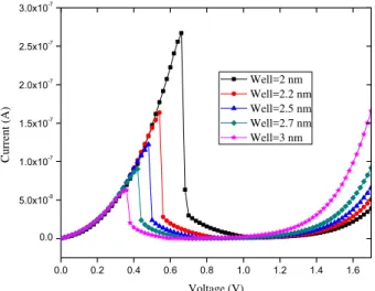
Well=2 nm Well=2.2 nm Well=2.5 nm Well=2.7 nm Well=3 nm
Fig. 2– Output current versus input voltage for different
quantum well width of RTD
In the RTDs the peak current (Ip) and the peak to valley current ratio (PVCR) are very important. At first we study the effect of the quantum well width on the performance of RTDs, so all parameters in Table 1 are kept constant but the well width is variable from 2 nm to 3 nm. It is clear from Fig. 2 and Table 2 that with in-crease of the well width (w), the peak current (Ip) is re-duced and the peak voltage Vp (the bias voltage associat-ed with the peak current Ip) shifts to the low voltage that reduces power consumption, because of the wide quan-tum well will push down the resonance energy level, thus the resonant tunnelling would happen at low bias voltage, moreover increasing the well width tends to decrease resonant energy levels. In consequence, a large well contains several resonant levels very close to each other, which may reduce the peak current. The valley current (Iv) that arise from the off-resonance is de-creased by increasing of the well width and the best val-ue of PVCR is obtained at well width of 2.5 nm.
Table 2– The value of Ip, Iv, PVCR and Vp for different
quan-tum well width of RTD
Well width (nm)
Ip (A) Iv (A) PVCR Vp (V)
DESIGN CONSIDERATIONS OF STRUCTURAL … J.NANO-ELECTRON.PHYS.7, 04026 (2015)
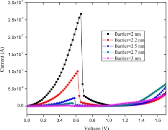
04026-3 Figure 3 shows I-V of RTD for different barrier width and the Table 3 shows the more detail of this I-V dia-gram. For Figure 3 all parameters in Table 1 are kept constant only the barrier width is varied from 2 nm to 3 nm. It is clear that with increase of the barrier width, the peak current, the valley current, the PVCR and the
Vp are decreased. Because the thicker the barriers are, the more difficult for the electrons to enter into or escape from the quantum well. Although the barrier width var-ies from 2 nm to 3 nm but the PVCR reduces from 271 to 16 and the peak current reduces from 2.7E – 7 A to 2.1E – 9 A, because the current varies exponentially with
er width, so these reduction are very high and the barri-er width is a sensitive parametbarri-er in RTD that must be considered.
0.0 0.2 0.4 0.6 0.8 1.0 1.2 1.4 1.6 0.0
5.0x10⁻⁸ 1.0x10⁻⁷ 1.5x10⁻⁷ 2.0x10⁻⁷ 2.5x10⁻⁷ 3.0x10⁻⁷
C
u
rr
en
t
(A
)
Voltage (V)
Barrier=2 nm Barrier=2.2 nm Barrier=2.5 nm Barrier=2.7 nm Barrier=3 nm
Fig. 3– Output current versus input voltage for different
barrier width of RTD
Table 3– The value of Ip, Iv, PVCR and Vp for different
barri-er width of RTD
Barrier width (nm)
Ip (A) Iv (A) PVCR Vp (V)
2 2.67E – 07 9.84E – 10 271.45 0.66 2.2 1.01E – 07 4.75E – 10 211.76 0.62 2.5 2.34E – 08 2.30E – 10 101.72 0.48 2.7 8.49E – 09 1.79E – 10 47.51 0.54 3 2.08E – 09 1.28E – 10 16.28 0.52
The spacer layer is important parameter that tunes the oscillation frequency in RTDs, moreover low doped or doped spacer layers are used in between the un-doped barrier / well / barrier region and the un-doped con-tacts to prevent diffusion of impurity atoms into the barriers and well. The impacts of spacer width on the performance of RTDs are indicated in Figure 4 and Table 4 as the width of spacer is varies from 5 nm to 20 nm by step 5. With increase of the spacer width, the peak current, the valley current, the PVCR are de-creased and the Vp is increased that needs more power consumption. Because the transit time for travel an electron from contact 1 to contact 2 is increased with increase of the spacer width that leads to reduction of peak current and PVCR.
Considering the fact that physically a contact is
de-fined as having infinite number of modes which makes it in equilibrium at all time. Each contact is treated as a big electron reservoir and it is maintained in equilib-rium with clearly defined Fermi level. Figure 5 shows the output current versus voltage for different contact width at constant contact doping concentration of 1 1018 cm – 3. Rest of the parameters in Table 1 are kept constant. The range of contact width is from 5 to 20 nm by step of 5. The Table 5 describes more details about Figure 5 and it is clear that with increase of the contact width the peak current and PVCR are almost identical, because the contacts are treated as a big elec-tron reservoir and only the peak voltage Vp is shifted to the larger voltage.
0.0 0.2 0.4 0.6 0.8 1.0 1.2 1.4 0.0
5.0x10⁻⁸ 1.0x10⁻⁷ 1.5x10⁻⁷ 2.0x10⁻⁷ 2.5x10⁻⁷ 3.0x10⁻⁷ 3.5x10⁻⁷ 4.0x10⁻⁷
C
u
rr
en
t
(A
)
Voltage (V)
Spacer=5 nm Spacer=10 nm Spacer=15 nm Spacer=20 nm
Fig. 4– Output current versus input voltage for different
spacer width of ETD
Table 4– The value of Ip, Iv, PVCR and Vp for different spacer
width of ETD
Spacer width (nm)
Ip (A) Iv (A) PVCR Vp (V)
5 3.87E – 07 1.29E – 09 299.32 0.54 10 2.89E – 07 1.06E – 09 272.39 0.60 15 2.67E – 07 9.84E – 10 271.45 0.66 20 2.45E – 07 9.24E – 10 265.13 0.72
0.0 0.2 0.4 0.6 0.8 1.0 1.2 1.4 1.6 0.0
5.0x10⁻⁸ 1.0x10⁻⁷ 1.5x10⁻⁷ 2.0x10⁻⁷ 2.5x10⁻⁷
C
u
rr
en
t
(A
)
Voltage (V)
Contact width=5 nm Contact width=10 nm Contact width=15 nm Contact width=20 nm
Fig. 5– Output current versus input voltage for different contact
M. CHARMI,M.H. YOUSEFI J.NANO-ELECTRON.PHYS. 7, 04026 (2015)
04026-4
Table 5– The value of Ip, Iv, PVCR and Vp for different
con-tact width at constant concon-tact doping concentration of 1E18 cm– 3
Contacts width (nm)
Ip (A) Iv (A) PVCR Vp (V)
5 2.63E – 07 9.86E – 10 266.79 0.56 10 2.66E – 07 9.74E – 10 272.74 0.62 15 2.67E – 07 9.84E – 10 271.44 0.66 20 2.62E – 07 9.83E – 10 266.36 0.66
To increase the current density through the device, heavily doped contacts are used which can supply large number of electrons. The impact of contact doping at constant contact width of 15 nm on the output parame-ters in RTD is investigated in figure and Table 6.
0.0 0.2 0.4 0.6 0.8 1.0 1.2 1.4 1.6 0.0
5.0x10⁻⁸ 1.0x10⁻⁷ 1.5x10⁻⁷ 2.0x10⁻⁷ 2.5x10⁻⁷ 3.0x10⁻⁷
C
u
rr
en
t
(A
)
Voltage (V)
Contact doping=1E17 cm-3 Contact doping=5E17 cm-3
Contact doping=1E18 cm-3 Contact doping=5E18 cm-3 Contact doping=1E19 cm-3
Fig. 5– Output current versus input voltage for different contact
doping concentration at constant contact width of 15 nm
Table 6– The value of Ip, Iv, PVCR and Vp for different
con-tact doping concentration at constant concon-tact width of 15 nm
Contacts
dop-ing
concentra-tion (Cm – 3)
Ip (A) Iv (A) PVCR Vp (V)
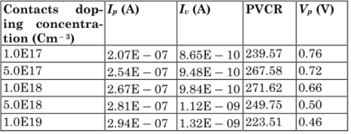
1.0E17 2.07E – 07 8.65E – 10 239.57 0.76 5.0E17 2.54E – 07 9.48E – 10 267.58 0.72 1.0E18 2.67E – 07 9.84E – 10 271.62 0.66 5.0E18 2.81E – 07 1.12E – 09 249.75 0.50 1.0E19 2.94E – 07 1.32E – 09 223.51 0.46
With increase of the doping large number of electrons can be participate in the output current so the peak cur-rent is increased and Vp the voltage associated with the peak current, is decreased. Therefore by increment of contact doping the power consumption is reduced. Alt-hough the peak current and valley current are increased with the increment of contact doping but there is a max-imum PVCR at contact doping of 1018 cm – 3 that is the best value for contact doping in the RTDs.
4. CONCLUSIONS
The novel confidants and design considerations of structural parameters in resonant tunneling diode have been studied using quantum simulation within the non-equilibrium Green’s function formalism. The effects of structural parameters on device performance are carried out in terms of peak current, peak to valley current ratio and Vp. The results show that the output characteristics of the RTD are more sensitive to the barrier width than the quantum well width and more sensitive to the contact doping to the contact width. We could also find proper selection of structural parame-ters for improving the performance of RTD.
REFERENCES
1. H. Eisele, Electron. Lett.46, s8 (2010).
2. C. O’Sullivan J. Murphy, Field Guide to Terahertz
Sources, Detectors, and Optics (SPIE Press: 2012).
3. S.J. Wei, H.C. Lin, IEEE J. Solid-State Circuit 27, 212 (1992).
4. S.J. Wei, H.C. Lin, R.C. Potter, D. Shupe, IEEE J. Solid-State Circuit28, 697 (1993).
5. T.P.E. Broekaert, B. Brar, J.P.A. Wagt, A.C. Seabaugh, T.S. Moise, F.J. Morris, E.A. Beam, G.A. Frazier, IEEE J. Solid-State Circuits33, 1342 (1998).
6. Y. Kawano, Y. Ohno, S. Kishimoto, K. Maezawa, T. Mizutani, Electron. Lett.38, 305 (2002).
7. U. Auer, W. Prost, G. Janßen, M. Agethen, R. Reuter, F.J. Tegude, IEEE J. Selected Topic. Quantum Electron.2, 650 (1996).
8. M. Bao, et al., IEEE J. Solid-State Circuits39, 1352 (2004). 9. N. Orihashi, S. Suzuki, M. Asada, Appl. Phys. Lett. 87,
233501 (2005).
10.N. Orihashi, S. Hattori, S. Suzuki, M. Asada, Jpn. J. Appl. Phys.44, 7809 (2005).
11.T.J. Shewchuk, P.C. Chapin, P.D. Coleman, W. Kopp, R. Fischer, H. Morkoç, Appl. Phys. Lett.46, 508 (1985). 12.H. Kanaya, R. Sogabe, T. Maekawa, S. Suzuki, M. Asada,
J. Infrared Milli Terahz Wave.35, 425 (2014). 13.S. Datta, Superlattice. Microstruct. 28, 253 (2000). 14.S. Datta, Quantum Transport: Atom to Transistor.
(Cam-bridge Univ. Press: Cam(Cam-bridge: 2005).
15.S. Datta, Electronic Transport in Mesoscopic Systems,
(Cambridge Univ. Press: Cambridge: 1995). 16.M. Goano, Solid-State Electron.36, 217 (1993).
17.P.V. Halen, D.L. Pulfrey, J. Appl. Phys.57, 5271 (1985). 18.Y. Wang, F. Zahid, Y. Zhu, L. Liu, J. Wang, H. Guo, Appl.
Phys. Lett.102,132109 (2013).
19.J. Batey, S.L. Wright, D.J. Dimaria, J. Appl. Phys.57, 484 (1985).