Brazilian Journal of Physics, vol. 29, no. 4, December, 1999 719
Spin-Dependent Resonant Tunneling in
Semiconductor Nanostructures
Erasmo A. de Andrada e Silva
Instituto Nacional de Pesquisas Espaciais CP515, 12201 S~ao Jose dos Campos, S~ao Paulo, Brasil
and Giuseppe C. La Rocca
Dipartimento di Fisica, Universita di Salerno 84081 Baronissi (Sa), Italia
and INFM, Scuola Normale Superiore, 56126 Pisa, Italia Received February 6, 1999
The spin-dependent quantum transport of electrons in non magnetic III-V semiconductor nanos-tructures is studied theoretically within the envelope function approximation and the Kane model for the bulk. It is shown that an unpolarized beam of conducting electrons can be strongly polar-ized in zero magnetic eld by resonant tunneling across asymmetric double-barrier structures, as an eect of the spin-orbit interaction. The electron transmission probability is calculated as a func-tion of energy and angle of incidence. Specic results for tunneling across lattice matched politype
Ga 0:47
In 0:53
As/InP=Ga 0:47
In 0:53
As/GaAs 0:5
Sb 0:5
= Ga 0:47
In 0:53
Asdouble barrier
heterostruc-tures show sharp spin split resonances, corresponding to resonant tunneling through spin-orbit split quasi-bound electron states. The polarization of the transmitted beam is also calculated and is shown to be over 50%.
The spin dependence of the electronic properties of articial nanostructures is one of the leading problems in the physics of electronic devices. The interest lays both on the improvementof actual devices, as theGaAs
polarized electron source (GaAs-PES) [1], and on the
search for new devices [2]. The eects of the spin de-gree of freedom on the electron quantum connement in III-V semiconductor nanostructures have been consid-ered experimentally [3] as well as theoretically [4, 5, 6] with good agreement. On the other hand, while a bet-ter understanding of the spin-dependent electron trans-mission through ferromagnetic metal thin layers [7] and tunnel junctions [8] has been recently obtained, very little has been done to elucidate the microscopic mech-anisms of electron spin polarized transport across non-magnetic semiconductor heterostructures [9].
The spin dependence of the electronic properties of such structures in zero applied magnetic eld originate from the spin-orbit interaction. The breaking of spin degeneracy in the conducting subbands when the sys-tem lacks inversion symmetry is of particular interest to electron both optical and transport properties [6]. Such
symmetry in commonGaAsheterostructures is in
gen-eral broken by both microscopic and macroscopic con-tributions to the electron potential. They are due to the dierent atoms in the unit cell and to the asymmetries in the band gap engineering, respectively, and produce dierent wave vector or k dependence of the energy
splitting between states with opposite spins. This in turn leads to spin-dependent electron transport eects of a somewhat dierent character.
In this paper we present the results of our investiga-tions on the eects of the macroscopic specular asym-metry on the spin dependent electron quantum (co-herent and vertical) transport in III-V nanostructures [10]. Such eects come from the so-called Rashba spin-orbit term, which, besides being adjustable according to the asymmetry fabricated, has been shown to be the strongest one in the case of structures with narrow gap materials [4, 6]. As the main result, we obtain a new spin dependent resonant tunneling eect that can in principle be used for electron spin polarization. The eects of the k
720 Erasmo A. de Andrada e Silva and Giuseppe C. La Rocca asymmetry are going to be treated in a separated
pub-lication.
The Rashba spin-orbit term can be derived from general symmetry arguments [11].It does not depend on the structure orientation with respect to the crystal axis; depends only on the angle between the growth
direction (^z) and the electron's wave-vector ~k, in fact it can be written as
Hso= ddz(z;E)j~kjsin = ddz(z;E)k
k: (1)
The coupling parameter as given by the eight band Kane model reads [6]
c
(z;E) = P2
2 (E,U(z)1,Ev(z) ,
1
E,U(z),Ev(z) + (z));
(2)
d
where U(x) is the electrostatic potential from the de-pletion layer or applied external eld, Ev is the edge
of the valence band, is the spin orbit splitting in the valence band and P is the interband momentum matrix element. Simple spin-dependent boundary con-ditions for the envelope functions can be derived in the presence of this term [6] and the problem of the spin-dependent quantum transport can be studied with the standard wave mechanics procedure.
Let's then consider the problem of an electron scat-tered by an ideal asymmetric double barrier potential with perfect translation symmetry along the plane of the interfaces, as illustrated in Figure 1. In the case of normal incidence ( = 0) the electron wave-vector has
no component parallel to the interfaces, i.e. kk = 0,
there is no spin-orbit interaction and one has the usual spin independent resonant tunneling problem. If in-stead the crossing is oblique ( 6= 0) the non zero
electron's kk is conserved and the result for the
trans-mission probability will depend on the orientation of the electron spin. Here we obtain such transmission probability from the solution of the stationary prob-lem HF = EF, for each spin orientation along
^y. In the at-band and zero-bias conditions, the en-velope function in the layer material j is of the form F = eik
kx(Aj e
ikjz + Bj e
,ik
jz), and the eective
Hamiltonian is given by:
c
H(E) = ,
~ 2
2 dzd m(E;z)1 dz + Ed c(z)Hso(E); (3)
where Ec(z) gives the conduction band edge prole and
1
m(E;z) = P
2 ~
2(
2 E,Ev(z) +
1
E,Ev(z),(z))
(4) is the inverse of the energy dependent eective mass as given by the same Kane model for the bulk.
Consider now an incoming electron with denite energy E and spin (+ or -, i.e. up or down with respect to a direction perpendicular to both ~kk and ^z), and solve for the spin dependent transmission coecient t. Using
standard transfer matrices the solution is straightforward:
t
0
= M2
eikzL 0
0 e,ik zL
M1
1 r
; (5)
where the Mj;j = 1;2 are the spin-dependent transfer matrices corresponding to the two dierent barriers, L is
the well width and kz =
q 2m0(E)
~ E cos() is the electron's wave-vector along the growth direction. The transfer
matrix are obtained directly from the spin-dependent boundary conditions [6] and can be written as: Mj = m
0mj
2kzjsinh(jdj)
e,ik
zdj 0
0 eikzdj
P Q
Q P
Brazilian Journal of Physics, vol. 29, no. 4, December, 1999 721 with
P = 2kmzj
0mj
1
tanh(jdj) + i[(2k
k ~
)2( 0
,j) 2+ ( k
2
z
m2 0
,
2
j
m2
j)] (7)
and
Q = 4k
zkk ~
2m 0
(0
,j) + i[(2k k ~
)2( 0
,j) 2
,( k 2
z
m2 0
+ 2
j
m2
j)]; (8)
d
where dj is the j barrier width,~k k =
p
2m0Esin is
the conserved momentum parallel to the interfaces and j=
q 2m
j ~
2 (Ejc
,E) + k
kis the decay coecient of the
evanescent wave inside the barrier. We remember that
fm 0;0
gandfmj;jg, the well and barrier
materialpa-rameters respectively, are energy dependent in accord to the expressions above. In the limitof 0= j= 0 (or
0= j= 0), i.e. no spin orbit interaction, the above
transfer matrix reduces to the usual spin-independent expression [12].
If one now consider an unpolarized beam of conduct-ing electrons it is possible to calculate the polarization of the transmitted beam dened by:
P(E;) = T+(E;) ,T
,(E;)
T+(E;) + T,(E;)
(9) where T = tt
is the spin dependent transmission
probability. The above obtained transfer matrix can be used also to calculate the spin dependent tunneling across single asymmetric barries, but the polarization of the transmitted beam one obtains is quite small [9]. A much larger polarization can be obtained with double barriers, as shown bellow.
As a practical and realistic example we have calculated the transmission probability and the polarization of the transmitted beam for a lattice matched politype Ga0:47In0:53As/
InP=Ga0:47In:53As/GaAs0:5Sb0:5/Ga0:47In0:53As
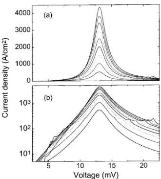
double barrier structure. As shown in Figure 2 we ob-tain sizable spin splittings in the sharp resonances. A splitting of a few meV is for instance observed between the transmission peaks connected with the resonant tunneling through the second quasi-bound subband. The eect is much smaller for tunneling through the ground subband in accord to the smaller spin-orbit splitting [6]. The corresponding polarization of the transmitted beam has been plotted in the lower part. The obtained polarization at resonance is in this case over 50%. Even larger polarizations can be obtained not only with the use of new material combinations, but also with a careful optimization of the asymmetric
structure parameters d1;d2and L. We have shown here
the results only as a function of energy for a xed , but it is clear that the results are similar as a function of for a xed energy.
Figure 1. Illustration of the spin polarized electron quan-tum transport problem discussed in the paper: resonant tunneling through asymmetric double barrier structures.
722 Erasmo A. de Andrada e Silva and Giuseppe C. La Rocca
Figure 2. Obtained spin-dependent electron transmis-sion probability for crossing an asymmetric double bar-rier Ga0:47In0:53As/InP=Ga0:47In0:53As/GaAs0:5Sb0:5/ Ga0:47In0:53As politype lattice matched structure,
illus-trated in Figure 1. The two doublets correspond to trans-mission through the ground and rst excited spin-split quasi-bound states respectively. In the lower panel is plot-ted the polarization of the transmitplot-ted beam. The bulk parameters used are the low temperature values reported in the Landolt-Borstain Tables. We usedL= 150A,=
4
and, for the InP and GaAs :5
Sb
:5 barriers, d
1 = 40 A, V
1= 0
:4eV andd 2= 40
A,V 2=
:15eV respectively. Thisworkwassupp ortedbyFAPESP(96/00058-1)
References
[1] See for instance,D.T. Pierce and R.J. Celotta in \Op-tical Orientation", F. Meier and B.P. Zakharchenya, eds.; Modern Problems in Condensed Matter Sciences Vol. 8 (Elsevier Sciences Publishers, 1984).
[2] See, for example, special issue of Physics Today, April 1995.
[3] J. Luo et al, Phys. Rev. B41, 7685 (1990); B. Das et
al, Phys. Rev. B39, 1411 (1989); B. Jusserand et al.,
Phys. Rev. B51, 4707 (1995), G. Engeles et al., Phys.
Rev. B55, R1958 (1997).
[4] P.V. Santos e M. Cardona, Phys. Rev. Lett. 72, 432
(1994); R. Winkler and U. Rossler Phys. Rev. B 48
8918 (1993) , P. Pfeer Phys. Rev. B55, R7359 (1997).
[5] E. A. de Andrada e Silva, Phys. Rev. B46, 1921 (1992)
[6] E. A. de Andrada e Silva, G. C. La Rocca and F. Bassani, Phys. Rev. B 50, 8523 (1994) and55, 16293
(1997).
[7] A. Filipe et al., Phys. Rev. Lett.80, 2425 (1998).
[8] S.T. Chui, Phys. Rev. B.55, 5600 (1997).
[9] see, for instance, A. Voskoboynikov, S. Shin Liu and C.P. Lee, Phys. Rev. B58, 15397 (1998).
[10] see, for a preliminary publication of the results, E. A. de Andrada e Silva and G. C. La Rocca, Phys. Rev. B
59, R15583 (1999).
[11] Yu. A. Bychkov and E. I. Rashba, J. Phys. C17, 6039
(1984).