Thin Films Growth by Electrochemical Process
*e-mail: [email protected], [email protected]
Article presented at the II SBPMat, Rio de Janeiro - RJ, 26-29 de Outubro/ 2003
Morphology and Stress Study of Nanostructured Porous Silicon as a
Substrate for PbTe Thin Films Growth by Electrochemical Process
Claudia Renata Borges Mirandaa,b*, Patrícia Guimarães Abramofa,c,
Francisco Cristovão Lourenço de Melob, Neidenêi Gomes Ferreirab*
a
Instituto Nacional de Pesquisas Espaciais INPE/LAS, C.P. 515, 122245-970 São José dos Campos - SP, Brazil
b
Centro Técnico Aeroespacial, Divisão de Materiais, AMR/IAE /CTA, 12228-904 São José dos Campos - SP, Brazil
c
Centro de Desenvolvimento de Tecnologia e Recursos Humanos, CDT, 12242-800 São José dos Campos - SP, Brazil
Received: February 17, 2004; Revised: August 3, 2004
Porous silicon layers (PSL) were produced by stain etching from a HF:HNO3 500:1 mixture with etching time varying in the range of 1 up to 10 min. The samples have presented nanometric porosity as a function of etching time, characteristic of heavily doped p type silicon. The residual stress and the correlation length of the layers were obtained through the analysis of the micro-Raman spectra using a phonon confinement model including a term to account for the amorphous phase. The residual compressive stress tends to increase as expected due to the contribution of smaller crystallites to be more representative as the etching time increases. PbTe thin films were electrodeposited on PSL from aqueous alkaline solutions of Pb(CH3COO)2, disodium salt of ethylendiaminetetraacetic acid (EDTA) and TeO2 by galvanostatic and potentiostatic method. It was also obtained nanostructured PbTe thin films with polycrystalline morphology evidenced by X-ray Diffraction (XRD) spectra. Scanning Electron Microscopy (SEM) analysis has demon-strated good films reproducibility with an average grain size of 100 nm.
Keywords: porous silicon, electrochemical, semiconductors
1. Introduction
Porous silicon layer has been exhaustively studied since the discovery of its room temperature luminescence by
Canham1, that turns it an interesting material for device
ap-plications. The mechanism of porous silicon formation, on p or n type of monocrystalline silicon wafer, is not yet to-tally understood and strongly depends on the crystal dop-ing level. In adittion, the use of PS layer as a substrate may provide a key for growing narrow gap semiconductors films
such as PbTe2. For infrared detectors development and
tech-nology from IV-VI films the state of the art is the use of silicon substrate, that has the advantage of operate at room temperature. The main difficult of growing IV-VI films on silicon substrate is the large lattice mismatch between Si and PbTe film. This lattice parameter difference, of around 19%, leads the production of lower quality and polycrystalline films with a poor adherence. For this pur-pose, it is necessary to perform a systematic study to find a
suitable PS layer that releases the thermal stress and the lattice mismatch between the lead salt films and the silicon bulk for infrared detectors applications2-4.
Raman spectroscopy has demonstrated to be a powerful technique for microstructural analysis and allows the stress and correlation length determination5-7. Tsu et al.8 reported
the first correlated study of Raman spectroscopy and pho-toluminescence (PL) of PSL and attributed the Raman peak shift of porous silicon to the effect of phonon confinement.
Min Yang et al.9 presented a Raman scattering study that
permits to extract a precise correlation between the Raman
shift and the peak width. Papadimitriou et al.6 have also
demonstrated the use of micro-Raman spectroscopy and the spatial correlation model to observe and separate structural and strain effects.
films growth from electrochemical technique. Micro-Ra-man spectroscopy and the spatial correlation model are used to estimate the residual stress of porous silicon layers ob-tained by stain etching, from heavily boron doped silicon
wafers p+ (100), as a function of the etching time. It is
dis-cussed the Raman peak shift and width, the amorphous sili-con sili-contribution and the correlation length for crystallites sizes of around 10 nm. This investigation was imperative for growing PbTe films on such PSL substrates by potentiostatic process and has allowed a better control of the film quality. Cyclic voltammetry was also used for study-ing the film deposition reaction and for findstudy-ing the appro-priate deposition potential range. The porous silicon and PbTe films were characterized by SEM, AFM, Raman spectroscopy, EDX and X-ray diffraction measurements.
2. Experimental
Monocrystalline p+ type silicon (100), boron doped with
concentration of 1018 atoms/cm3 was used for preparing PSL.
Chemical etching (stain etching) was made from different concentrations of nitric and hydrofluoric acids with rations
between 50:1 and 500:110. Strong dependence of the
incu-bation time on the type and doping concentration of silicon
wafer has been observed11. This effect was minimized by
adding, into the solutions, sodium-nitride with a concentra-tion between 0.1 and 0.6 g/L in order to reduce the
incuba-tion time of PSL formaincuba-tion12. The PSL morphology was
analyzed by SEM with a LEO 435 system and AFM meas-urements with a Shimadzu SPM 9500J3 equipment by work-ing at dynamic mode.
Lead telluride (PbTe) thin films were electrodeposited
by using a solution containing dissolved TeO2,
Pb(CH3COO)2, and EDTA disodium salt in deionized
wa-ter. The films were grown at potentials of 0.85 and 0.98 V × Ag/AgCl, confirmed by previous cyclic voltammetry
meas-urements. The solution was formulated from 0.001 M TeO32-,
0.1 M Pb(CH3COO)2, and 0.13 M EDTA, which was also
used to complex Pb2+ in order to prevent the spontaneous
precipitation of Pb(OH)2. The pH = 9 solution was adjusted
with NaOH addition. At this pH tellurium is expected to be in the form TeO32- 13.
A Microquímica MQPG-01 potentiostat with three elec-trode cell was used for both the cyclic voltammetry meas-urements and the electrodeposition of PbTe films. The elec-trodes were porous silicon substrates as a working electrode, Pt disk as a counter electrode and Ag/AgCl as a reference electrode. A voltage scan rate of 100 mV/s was used in cy-clic voltammetry. Measurements were carried out from
al-kaline solutions at pH 9 containing 0.05 M PbEDTA2-,
0.001 M TeO32-, and mixtures of them on silicon substrates.
Both electrodeposition and cyclic voltammetry were car-ried out at room temperature and in unstirred solutions. The
surface morphology and compositions (EDX) of the films was analyzed by SEM images using a LEO 435 system. Crystal structures were examined by a Philips PW 1830 X-ray diffractometer.
3. Results and Discussion
3.1. Residual stress in nanostructured porous silicon layers
For the stress evaluation, a single micro-Raman meas-urement point is not representative due to the presence of inhomogeneous stress. For this reason, we used the sum-mation method, which consists in the sumsum-mation of a large number of spectra from a selected area of the sample. In our case, five points were chosen in a central area of 4.0
mm2 of the sample, and for each point the spectra were
scanned five times to improve the statistics of the Raman data. Raman shift is normally used to estimate the residual
stress in PSL5,6. Besides, if the Raman is described
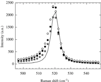
theoreti-cally, additional information can be obtained such as the crystallite size and shape, and the fraction of amorphous phase. Fig. 1 shows the Raman spectra in the vicinity of the Si peak for three porous silicon layers samples with etching time of 2, 5 and 8 min. The spectrum corresponding to the monocrystalline silicon is also plotted in the figure as a ref-erence (solid line). A broadening and an asymmetry can be observed in the Raman spectra of the PSL compared to the monocrystalline Si peak.
Raman spectra of PSL was analyzed by using a correla-tion length model developed by Richter et al.14. In this model,
disorder or finite size effects may result in a relaxation of the momentum conservation rule leading to a downshift and
Figure 1. Raman spectra measured in the vicinity of the Si peak
Thin Films Growth by Electrochemical Process
an asymmetric broadening of the first order Raman peak. This model was improved afterwards by Campbell and
Fauchet7 to calculate separately the correlation length L for
three micro-crystals shapes, namely: spherical, columnar and thin slab. The intensity of the first order Raman band of porous silicon is calculated by the sum of two components: a band given by the phonon confinement model (Richter) and a Gaussian distribution to account for amorphous sili-con5,15 through the following relation:
I(ω) = A
(1)
where ω (q) = ω
0-120(qa0/2π)
2 is the phonon
disper-sion relation, q is the wave vector, a0= 0.54 nm is the lattice
parameter of bulk silicon, Γ
0 ~ 4.5cm
-1 is the Raman
intrin-sic line width of crystalline silicon, ω
0 = 520.5 cm -1 is the
wave number of the first order Raman band in the absence of disorder effects and stress effects, and C(q) are the Fourier
coefficients of the phonon confinement7. The Fourier
coef-ficients are given as a function of the correlation length or the theoretical crystal size L. The Gaussian band shape
cor-responding to the amorphous silicon is centered at ω
a with
a full width at half maximum Γ
a.
The Raman spectrum of each sample of the set of PS layers with etching time varying from 1 to 10 min was fit-ted by the expression described above, assuming a colum-nar crystallite shape. The correlation length (L), the linewidth (Γ
0), the frequency shift (ω0), the linewidth and the frequency
shift of the amorphous silicon were used as free parameters for the fitting. The columnar crystallite size decreases from 13 to 9 nm as the etching time increases from 1 to 10 min. The residual stress can be obtained from the difference be-tween the observed frequency of the first order Raman peak (ω
obs), which is shifted in relation to the crystalline Si
natu-ral frequency (ω
0), and the confinement frequency (ωconf)
obtained from the theoretical evaluation of the Raman
spec-trum. Therefore, the stress induced shift is given by6
∆ω
stress = ωobs - ωconf (2)
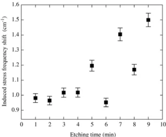
Figure 2 depicts the stress induced shift for the porous silicon samples as etching time increases. Note that the stress induced shift increases as the correlation length decreases. However, the stress induced shift does not have a monotonic behavior for etching times higher than 4 min, where is ob-served an oscillation in the induced stress shift.
The morphology of PSL was also observed by AFM analysis. Details of this subject were discussed in a
previ-ous work16. The nanocrystalline size and size distribution
depend on the experimental parameters such as substrate level doping and type and also the acid concentration. A
characteristic of p+ type silicon, heavily doped, is the
for-mation of a columnar-type structure of few nanometers. For few min of etching time it was observed just a small rough-ness correspond to the initial stage of the etching and a nanoporous formation. The samples presented a non-uni-form porous distribution with crystallites sizes of around 10 up to 40 nm. In fact, AFM images revealed a fractal struc-ture of the surface more and more inhomogeneous as the etching time increases. This behavior was attibuted a simul-taneous and competitive process while the crystallites become larger because new smaller crystallites always will appear during the etching. This observed morphology variation con-firms the oscillation behavior for induced stress from Raman spectra evidenced in Fig. 2. These results were also confirmed by X-ray diffraction and reflectivity techniques for strain and
porosity evaluation on PSL described elsewhere17.
3.2. PbTe electrodeposition
The process for obtaining semiconductors films by electrodeposition presents many advantage compared to the conventional techniques for epitaxial growth. This is a
sim-ple and low cost thin film method18. Electrodeposition can
be carried out using substrates with different sizes and shapes. Reactions involved occur closer to the equilibrium and the deposition process may be controlled more easily than in many high temperature gas phase methods as HWE or Fresh Evaporation. Besides, it is not necessary the use of toxic gaseous precursors unlike in chemical gas phase meth-ods. The only major limitation of electrodeposition is the use of a conductive substrate, which is eliminated in the
Figure 2. Stress induced shift (squares) as a function of the
case of PSL. Some authors13,19,20 have studied the PbTe
electrodeposition by using different substrates. It was also made cyclic voltammetry measurements for studying the film deposition reactions. This study was important for analyzing the reduction/oxidation peaks of lead and tellu-rium. The results have shown that the work potential range between - 0.7 to - 0.95 V × Ag/AgCl correspond to the nec-essary potential for the film growth.
PbTe thin films were deposited by using PSL as work electrode, Pt disk as a counter electrode and a reference electrode of Ag/AgCl. The potential range that promote epitaxial growth is very narrow (0.05 V) and a very small current variation provokes too large a potential variation. Potentiostatic growth in the range of - 0.85 and - 0.98 V × Ag/AgCl are closer to lead oxidation potential and has per-mitted a better deposition control. SEM surface morphol-ogy of the PbTe film electrodeposited on PSL substrates etched durant 3 min has evidenced a polycrystalline and nanostructured grains with an average size of 100 nm. The images on Figs. 3a and 3b correspond to films grown dur-ing 30 min by potentiostatic mode with 0.98 V × Ag/AgCl. The white regions on the figures also present a PbTe film composition confirmed by EDX analysis.
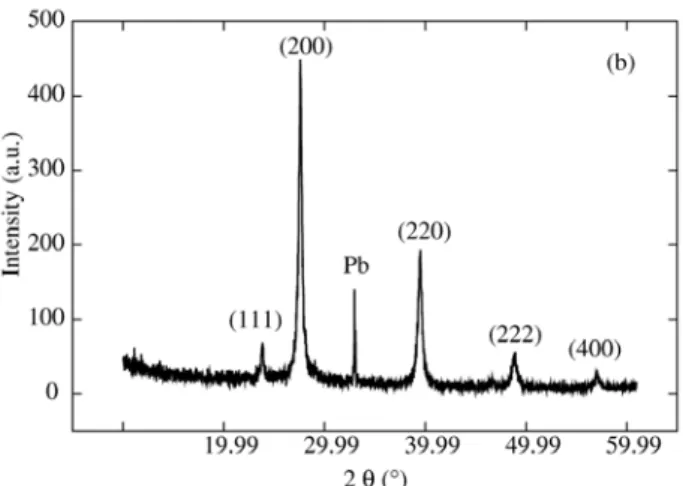
X- ray diffraction measurements allow us to obtain quan-titative information about the epitaxial growth deduced from a large surface area. X-ray diffraction spectra for PbTe films are shown on Fig. 4. The films presented a polycrystalline structure and can be observed the PbTe peaks (200), (220), (222) e (400). It is also observed lead peak. For films grown from potentiostatic process this lead peak present less in-tensity and did not appear in some films. These spectra are
similar to the PbTe films on SnO2 obtained by Saloniemi
et al.13 and refer to the cubic PbTe. This lead contamination
is probably due to the films to be formed in the higher nega-tive potential that makes favorable only the lead deposition. This result confirm that the control of deposition potential strongly affect the film stoichiometry.
4. Conclusions
Raman spectroscopy was used as a suitable technique for establishing the relationship between the Raman peak shift and peak width for PS layers. From the measured spec-tra the residual stress was evaluated as a function of the etching time. The competitive process between the increase of the crystallites and surface porosity is detected by the Raman spectra and gives a significant contribution when the density of smaller crystallites is higher and depends on the etching stage for each sample analyzed. The results also evidence an almost constant and small residual stress val-ues for the first 4 min of etching time, originated from nanostructures of singular uniformity.
PbTe thin films were deposited potentiostatically by
Figure 4. X-ray diffraction of PbTe thin film electrodeposited at
potential of 0.98 V × Ag/AgCl by potentiostatic process on PSL etched during 3 min.
Figure 3. SEM images for PbTe thin films electrodeposited on
PSL etched during 3 min at potential of 0.98 V × Ag/AgCl. a) 6.000 X; b) 18.000 X.
(a)
Thin Films Growth by Electrochemical Process
electrochemical process on PSL with a relative success. For potentiostatic process the film growth was carried out at potentials of 0.85 and 0.98 V × Ag/AgCl. The films pre-sented polycrystalline morphology with a strong depend-ence of the deposition rate, controlled by the range of depo-sition potential that influences the film epitaxy. It was not observed a preferential orientation from X-ray diffraction measurements besides the identification of lead peaks. The results may be considered promising by to be an innovative process for growing PbTe films. This work associated the use of PSL for obtaining a PbTe and minimizing the intrin-sic stress in such a film usually presents when monocrystalline silicon is used as substrate.
References
1. Canham, L.T. Appl. Phys. Lett., v. 57, n. 10, p. 1046-1048, 1990.
2. Zimin, S.P.; Preobrazhensky, M.N.; Zimin, D.S. et al.,
Infrared Phys. and Technol. v. 40, p. 337-342, 1999.
3. Bondarenko, V.P.; Vorozov, N.N.; Dikareva, V.V. et al.,
Technol. Phys. Lett., v. 20, n. 10, 51-55, 1994.
4. Zimin, S.P.; Zimin, D.S.; Saunin, I.V. et al., Inorganic
Mat., v. 34, n. 5, p. 440-441, 1998.
5. Manotas, S.; Agulló-Rueda, F.; Moreno, J.D.; Ben-Hander, F.; Guerrero-Lemus, R.; Martínez-Duart, J.M.,
Phys. Stat. Sol, v. 182, p. 245-248, 2001.
6. Papadimitriou, D.; Bitsakis, J.; López-Villegas, J.M.; Samitier, J.; Morante, J.R.; Thin Solid Films, v. 349, p. 293-297, 1999.
7. Campbel, I.H.; Fauchet, P. M. Solid State Commun., v. 58,
n. 10, p. 739-741, 1986.
8. Tsu, R.; Shen, H.; Dutta, M. Appl. Phys. Lett., v. 60, n.1, p. 112-114, 1992.
9. Yang, M.; Huang, D.; Hao, P.; Zhang, F.; Hou, H.; Wang, X. J. Appl. Phys., v. 75, n. 1, p. 651-653, 1994. 10. Vazsonyi, É.; Szilágyi, E.; Petrik, P.; Horváth, Z.E.;
Lohner, T.; Fried, M.; Jalsovszky, G. Thin Solid Films, v. 388, p. 295-302, 2001.
11. Steckl, A.J.; Xu, J.; Mongul, H.C.; Mogren, S. Appl.
Phys. Lett., v. 62, n. 16, p. 1982-1984, 1993.
12. Kelly, M.T.; Chun, J.K.M.; Bocarsly, A.B. Appl. Phys.
Lett., v. 64, n. 13, p. 1693-1695, 1994.
13. Saloniemi, H.; Kanniainen, T.; Rtala, M.; Leskela, M.
Thin Solid Films, v. 326, p. 78-82, 1998.
14. Richter, H.; Wang, Z.P.; Ley, L. Solid State Comun., v. 39, n. 5, p. 625-629, 1986.
15. Sui, Z.; Leong, P.P.; Herman, I.P.; Higashi, G.S.; Temkin, H. Appl. Phys. Lett., v. 60, n. 17, p. 2086-2088, 1992. 16. Abramof, P.G.; Ferreira, N.G.; Beloto, A.F.; Ueta,A.Y.
Journal of Non-Crystalline Solids, v. 338-340, p.
139-142, 2004.
17. Abramof, P.G.; Ferreira, N.G.; Beloto, A.F.; Ueta, A.Y.
10th ISMANAN, Foz do Iguaçu, Brazil, p. 110-111,
Au-gust/2003.
18. Rajeshwar, K. Adv. Mater., v. 4, n. 1, p. 23-29, 1992. 19. Dimova-Malinovska, D.; Sendova-Vassileva, M.;
Kamenova, M.; Tzenov, N.; Tzolov, M. Vacuum, v. 47, n. 9, p. 1133-1138, 1996.
20. Saloniemi, H.; Kemel, M.; Ritala, M.; Leskela, M. J.