Hydroxyapatite screen-printed thick films: optical
and electrical properties
C.C. Silva
a, H.H.B. Rocha
a, F.N.A. Freire
b, M.R.P. Santos
a, K.D.A. Saboia
a,
J.C. G´oes
a, A.S.B. Sombra
a,∗aLaborat´orio de Telecomunica¸c˜oes e Ciˆencia e Engenharia de Materiais (LOCEM), Departamento de F´ısica,
Universidade Federal do Cear´a, Campus do Pici, Caixa Postal 6030, 60455-760 Fortaleza, Cear´a, Brazil
bDepartamento de Quimica Orgˆanica e Inorgˆanica-UFC, Caixa Postal 6030, CEP 60455-760, Fortaleza, Cear´a, Brazil
Received 16 September 2004; received in revised form 11 January 2005; accepted 21 January 2005
Abstract
In this paper, we did a study on the structural and electrical properties of bioceramic hydroxiapatite (HA) thick films. The films were prepared in two layers using the screen-printing technique on Al2O3substrates. Mechanical alloying has been used successfully to produce
nanocrystalline powders of hydroxyapatite to be used in the films. We also look for the effect of the grain size of the HA in the final properties of the film. The samples were studied using X-ray diffraction (XRD), scanning electron microscopy (SEM), energy-dispersive spectroscopy (EDS), infrared and Raman scattering spectroscopy and electrical measurements. We did a study of the dielectric permittivity and the loss of the films in the radio-frequency of the spectra. The X-ray diffraction patterns of the films indicate that all the peaks associated to HA phase is present in the films. One can notice that, for all the films there is a decrease of the DC (dielectric constant) with the increase of the frequency. The values of the dielectric constant of the films are in between 4 and 9 (at 1 kHz), as a function of the flux concentration. The loss is decreasing as we increase the frequency for all the films. These results strongly suggest that the screen-printing HA thick films are good candidates for applications in biocompatible coatings of implant materials.
© 2005 Elsevier B.V. All rights reserved.
Keywords: Screen-printed thick films; Scanning electron microscopy; Raman scattering spectroscopy
1. Introduction
Hydroxyapatite, (HA, Ca10(PO4)6(OH)2) is widely used
in reconstructive orthopedic and dental surgery, both as mas-sive filling[1]of bone gaps and as a surface coating. In the latter case it promotes adhesion between prostheses and bone [2]. This substance is present in substantial amounts in the mineralised tissue of the vertebrates—60–70% of the mineral phase of the human bone[3]. In order to propose the biosyn-thetic process of the bone, the synthesis of HA was developed in this work. The human bone is formed basically by an or-ganic phase and other mineral phases. In the oror-ganic phase, the fibers of collagen serve as a matrix for the precipitation
∗Corresponding author. Tel.: +55 85 2889909; fax: +55 85 2889450.
E-mail address:[email protected] (A.S.B. Sombra).
URL:www.locem.ufc.br (A.S.B. Sombra).
of HA, determining the structure of the crystals. The colla-gen gives the bone its elastic resistance. The mineral phase is formed by HA.
Several processes[4,5]are used to produce HA of wide ap-plication as a temporary substitute for the human bone[5–9]. Hydrothermal synthesis is characterised by the reaction of aqueous solutions in closed recipients under controlled tem-perature and/or pressure. The temtem-perature can be elevated above the boiling point of the water, reaching the pressure of vapour saturation. One specific method of hydrothermal syn-thesis consists of submitting an aqueous solution containing Ca2+ and PO43− to high temperatures (200–500◦C). Thus,
a calcium phosphate compound is obtained which is able to maintain the morphological structure of the original material. The hydrothermal method has been widely used[9]for the preparation of materials for prosthetic purposes. These ma-terials are attractive for various applications include coatings
of orthopedic and dental implants, alveolar ridge augmen-tation, maxillofacial surgery, otolaryngology, and scaffolds for bone growth and as powders in total hip and knee surgery.
The HA ceramic, however, are much more brittle than liv-ing bone and ordinary bioceramics, such as tricalcium phos-phate (TCP), alumina ceramics (␣-Al2O3) etc. Under this
view, much effort has been devoted in recent years to the development of processing methods to deposit HA on cor-rosion resistant alloys. Recent advancements in synthesis of HA coatings include eletrophoretic deposition[10,11], elec-trochemical deposition[12], laser pulse deposition[13], ion beam deposition[14]and more recently, sol–gel deposition [15,16]. The sol–gel approach received more attention than others over the past 10 years because of its low temperature nature and ease of processing and forming. Others deposi-tion methods include for the HA thin film have been reported which include sputtering[17]. Recently, the pulsed laser de-position (PLD) methods has been applied to produce pure crystalline HA thin films[18,19].
In this work, we report the application of mechanical alloying technique to produce HA, from elementary pow-ders. The advantage of this procedure remains on the fact that melting is not necessary; the powders are nanocrys-talline and exhibits extraordinary mechanical properties [20–22].
It can also be easily shaped (injected, compacted, etc.) into any geometry. The production, and the study of the properties of HA ceramics is important in view of possible applications of HA in the area of orthopedics and dentistry emerges as one of the most important applications of this material.
Mechanical alloying is a powerful technique to obtain any quantity of powder with controlled microstructure [22]. Nowadays the technique is used in a large range of commercial products; moreover, most of these applications are on metallic domain. The mechanical alloying technique was already used, by our group, to obtain nanocrystalline ferroelectric ceramics of lithium niobate LN (LiNbO3)[20].
Lithium Niobate-LN is a ferroelectric material with a trigonal crystal structure, with melting point at 1253◦
C and Curie temperature at 1210◦
C. It is characterised by large pyroelec-tric, piezoelecpyroelec-tric, electro-optic, photo-elastic coefficients and is naturally birefringent. Furthermore, the technique is very effective to produce nanocrystalline piezoelectric ceramics.
In this paper, we describe the preparation of HA thick films, prepared from a nanocrystalline HA ceramic obtained by mechanical alloying. The HA thick film was prepared over a thick film of silver. The optical and electrical properties are directly connected to structural data that could be obtained, associated to the crystalline structure. The structural properties of the films are discussed with emphasis on the electrical properties. These properties are important in view of possible applications of screen-printing HA thick films in biocompatible coatings of implant materials.
2. Experimental procedure
2.1. HA nanocrystalline powder
In this paper, mechanical alloying has been used success-fully to produce nanocrystalline powders of hydroxyapatite (HA) using the procedure[22]:
10Ca(OH)2+3P2O5IMPACTS−→ Ca10(PO4)6(OH)2+9H2O
Commercial oxides Ca(OH)2 (Vetec, 97% with 3% of
CaCO3), P2O5 (Vetec, 99%), were used in the HA
prepa-ration[22]. For this reaction the material was ground on a Fritsch Pulverisette 6 planetary mill with the stechiometric proportionality between the oxides given in above equation. Milling was performed in sealed stainless steel vials and balls under air, with 370 rpm as rotation speed. The powder mass to the ball mass ratio used in all the experiments was near 1/9. To avoid excessive heat the milling was performed in 60 min milling steps with 30 min pauses. Mechanical alloying was performed for 60 h of milling to produce the ceramic HA3.
2.2. Paste preparation
The paste was prepared from the suspension of organic material (resin, organic solvent and some additive to improve rheological behavior of the paste) and powders (HA), in re-lation 30:70. The organic part used in the film preparation was chitosan. Chitosan is a polymer, which contains-1-4 linked 2-amino-2-deoxy-d-glucopyranose repeat units and is
readily obtained by theN-deacetylation of chitin, a naturally abundant polysaccharide. This biopolymer is the structural component of the cuticles of crustaceans, insects, and mol-lusks and is also found in the cell of some microorganisms. A number of biomedical applications have also been envis-aged. Chitosan and its derivatives have explored as mem-branes for dialysis, wound healing accelerators and carriers for controlled drug delivery[23]. To have a better adhesion between paste and substrate (Al2O3), it was added a low
tem-perature melting glass (boro-phosphate glass, with melting temperature between 400 and 500◦C) in powder form. The concentration of the glass in the total mass of the samples is indicated by the referenceYin the indication of the samples (seeTable 1). The samples are indicated by HA3GY, where Y= 5, 10, 15, 20 and 25% is the indication of the glass pres-ence (%) in the total mass of the powder, used in the film preparation.
2.3. Substrates and electrodes
Alumina substrates (Al2O3) were used as a commercial
Table 1
Dielectric permittivity measurements (K), thickness (e), dielectric loss (D), and the crystallite size obtained from the X-ray diffraction (Fig. 2) of the thick films samples
Samples Thickness (m) K[ε33 ′
/ε0] (1 kHz) D(ε33 ′′
/ε33 ′
) (1 kHz) Crystallite size (nm) Ca/P mass ratio
HA3 (powder) 38.9 2.10
HA3G5 351 4.96 0.27 46 1.62
HA3G10 328 5.75 0.10 44 2.37
HA3G15 305 5.38 0.58 47.5 2.37
HA3G20 328 8.73 0.48 46.3
HA3G25 325 8.22 0.72 42.5
Mass relation Ca/P obtained from energy-dispersive spectroscopy (expected value for HA is 2.15) for the HA3 ceramic and thick films HA3G5, HA3G10 and HA3G15.
2.4. Preparation of the films
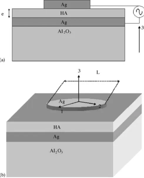
The botton electrode (Ag) was screen printed on the Al2O3
substrate and fired at 850◦C for 1 h. On the fired elec-trode, a HA layer was screen printed and sintered at for 1 h. After firing the dielectric layer, the upper electrode (Ag) was deposited, and after that dried and fired at the same temperature-time regime as for the bottom electrode. The obtained films usually had thickness that ranged from 20 to 400m (m = 10−6m), depending on the number of layers.
All the films used in these measurements were composed of two layers. For the films in the series HA3G(Y) A (see Table 1), the film was subjected to the firing process: 100◦
C for 1 h + 400◦
C for 1 h + 700◦
C for 1 h (first layer), 100◦ C for 1 h + 400◦C for 1 h + 700◦C for 1 h (second layer).
Fig. 1. A rectangular coordinate assigned to the sample for the measurement of piezoelectric and dielectric constant in the thick film structure.
2.5. X-ray diffraction
The X-ray diffraction (XRD) patterns were obtained at room temperature (300 K) by step scanning using powdered samples. We used five seconds for each step of counting time, with a Cu K␣tube at 40 kV and 25 mA using the geometry of Bragg-Brentano. The analysis of the crystallite size (Lc)
of the HA phase has been done for all samples using the Scherrer’ equation,
Lc= kλ βcosθ
wherekis the shape coefficient (value between 0.9 and 1.0);λ, the wave length;β, the full width at half maximum (FWHM) of each phase andθ, the diffraction angle. For this purpose, we chose the single peak near 25.8 degree within the pattern and according toP63/mspace group of HA. We have used
the LaB6(SRM 660—National Institute of Standard
Technol-ogy) powder standard pattern to determine the instrumental width (winst= 0.087◦) and afterward to calculate the
crystal-lite size via Eq. (1). Theβparameter has to be correct using the following equation:
β=
w2exp−w2inst (1)
wherewexpcorrespond to experimental FWHM obtained for
each sample. The crystallite size for the milled ceramic and for the film was obtained, assuming coefficientk= 1.
2.6. Scanning electron microscopy
The photomicrograph of the films of HA, were obtained on a Scanning Electron Microscope, Phillips XL-30, operating with bunches of primary electrons ranging from 12 to 20 keV, in rectangular lyophilized samples, covered with a layer of carbon of 30 nm of thickness.
2.7. Raman spectroscopy
2.8. Infrared spectroscopy
The infrared spectra (IR) were measured using KBr pellets made from a mixture of powder for each glass composition. The pellet thickness varied from 0.5 to 0.6 mm. The IR spectra were measured from 400 to 4.000 cm−1with a Nicolet 5ZPX
FT-IR spectrometer.
2.9. Dielectric measurements
The dielectric measurements were obtained from a HP 4291 A Material Impedance Analyzer in conjunction with a HP 4194 Impedance Analyzer, which jointly cover the region of 100 Hz to 1.8 GHz. InFig. 1, one has the sample geometry we used for the dielectric measurements. Rectangular coordi-nates are assigned to the samples as shown inFig. 1. The 1–2 plane is the sample plane, and the 3 axis is perpendicular to the plane of the sample. The electrodes are circular (Ag) pre-pared using the screen-printing technique. Our study is trying to understand the dielectric properties of the HA thick films. We prepared different samples with different glass concen-tration on the HA films. The glass concenconcen-tration was changed from 5 to 25% in the film preparation (seeTable 1). For the HA powder one prepare a nanocrystalline powder prepared by mechanical alloying. We did a study of the dielectric per-mittivity (K) and loss (D), films. The role played by firing process of the film and the role played by the amount of glass in the structural properties of the film is also discussed.
3. Results and discussion
3.1. X-ray diffraction
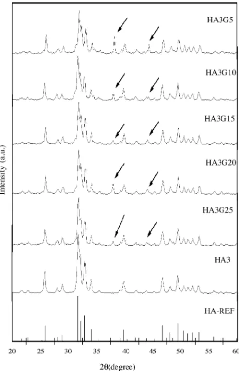
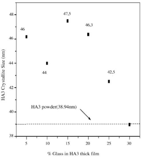
Fig. 2shows X-ray diffraction patterns of the films to-gether with the XRD of the powder (HA3) used in the film preparation (seeTable 1). The XRD of the powder HA3 shows that all the peaks associated to HA is present (seeTable 1). For this ceramic the crystallite size is estimated in 38.9 nm (seeTable 1). In the same figure, one starts with the XRD of sample HA3G5. For this sample one can easily notice all the peaks associated to HA. However, the crystallite size associ-ated to HA is around 46 nm (seeTable 1). One can associate the increase of the grain size to the firing process that the film was submitted. One can also notice the presence of two little peaks (indicated by arrows in the figure), that are prob-ably associated to the presence of the flux material (powder glass) that was used to improve the adhesion between the paste and the substrate. These peaks are probably associated to the presence of the glass in the film structure. If one starts increasing the presence of the glass (G= 10, 15, 20 and 25%) these peaks are still present (seeFig. 2). One can also con-clude the HA crystallite size is in average around 46 nm for all the series (seeTable 1andFig. 3). The HA crystallite size seems to be less affected by the presence of the flux material.
Fig. 2. XRD patterns of the ceramic HA3 and thick films HA3G5, HA3G10, HA3G15, HA3G20 and HA3G25 and literature data for HA[13].
One can also associate the increase of the grain size to the firing process that the film was submitted. The crystallite size of the HA is around 46 nm in the films of this series.
3.2. Scanning electron microscopy
Fig. 3. Crystallite size of the HA in the ceramic HA3 and thick films HA3G5, HA3G10, HA3G15, HA3G20 and HA3G25 (data fromFig. 1).
phosphorus and calcium. For the films HA3G5, HA3G10 and HA3G15 one has the same elements. The EDS of a crystal, present in the ceramic HA3 showed a mass ratio of Ca/P around 2.1 (seeTable 1). The theoretical expected value for HA is around Ca/P = 2.15. For the film with higher glass content (HA3G10 and HA3G15) it was observed a Ca/P ratio around 2.3 (seeTable 1). For the HA3G5 film the Ca/P ratio is around 1.62, which is below the expected value of 2.15. The presence of others phases in the HA film (detected in the X-ray analysis) could be the reason for this deviation. For the
Fig. 4. Scanning electron photomicrograph of the HA3G5 thick film (5000×).
Fig. 5. Scanning electron photomicrograph of the HA3G10 thick film (5000×).
HA3G15 (seeTable 1andFig. 8), the mass ratio expected is around Ca/P = 2.15 and one actually has Ca/P = 2.37, which is a reasonable agreement with the expected value.
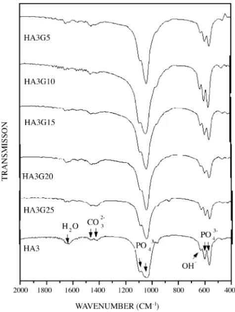
In Fig. 9, one has the IR spectra of the thick films HA3G5, HA3G10, HA3G15, HA3G20, HA3G25 along with the spectrum of HA ceramic HA3. In this spectra, the characteristic absorption bands of HA are observed[22,23]. The bands at 565 cm−1(ν
4), 603 cm−1(ν4), 1040 cm−1(ν3),
a shoulder at 961 cm−1(ν
1), can be attributed to the PO43−
ion. The band at 874 cm−1attributed to CO
32−. Vibrations
associated to OH−are detected by the band at 634 cm−1. The
bands at 1419 cm−1and 1452 cm−1arise from vibrations of
the CO32−ions (seeTable 2). The presence of carbon modes
in commercial sample is an indication that carbon is also an
Table 2
IR lines and Raman lines obtained from the samples HA3, HAG5, HAG10, HAG15, HAG20 and HAG25 compared with data of references
HA[27] Carbonated apatite[27] HA3 HA3G5 HA3G10 HA3G15 HA3G20 HA3G25
Raman (cm−1)
ν3(PO4) 1075 1075 1079 1080 1080 1081 1074 1073
ν3(PO4) 1046 1046 1047 1052 1052 1053 1047 1049
ν1(PO4) 962 962 963 967 967 967 962 962
ν4(PO4) 593 592 591 597 596 596 590 589
ν4(PO4) 581 585 585 584 579 579
ν2(PO4) 447 448 – – –
ν2(PO4) 432 432 430 436 434 438 427 430
IR (cm−1)
ν3(CO3−2) 1500 1467 1461 1465 1461 1461 1463
ν3(CO3−2) 1415 1421 1433 1415 1433 1425 1421
ν3(PO4−3) 1097 1091 1093 1091 1089 1091
ν3(PO4−3) 1065 1060 1047 1043 1047 1043 1043 1045
ν1(PO4−3) 962 961 962 968 962
ν2(CO3−2) 873 874 875
OH− 631 634 634 632 632 632 636 634
ν4(PO4−3) 602 605 603 603 603 603 601 601
ν4(PO4−3) 565 568 568 569 569 569 569 570
impurity in this sample from the preparation process, which is not detected in the X-ray.
IR spectra of reaction 3 show the absorption associated to CO32−at mode 1467 cm−1 and 1421 cm−1. The modes
565 cm−1(ν
4), 603 cm−1(ν4) are also in a very broad band
centered at 562 cm−1. InTable 2, one has the IR and Raman
modes of HA and carbonated HA and the modes observed in this work.
In Fig. 10, one has the Raman spectra of the HA3 ceramic together with the Raman spectra of the thick films. The space group of HA has been determined by X-ray diffraction methods to beP63/m, the same as fluorapatite,
but theoretical considerations suggests the space group of HA to be P63[24]. The spectrum of HA, contained bands
associated to internal vibrational modes and bands due to
Fig. 7. Scanning electron photomicrograph of the HA3G25 thick film (5000×).
hydroxyl ion stretching and librational modes [23,25–27]. At room temperature apart from the hydroxyl bands, one has ν1(PO4) bands, ν2(PO4), ν3(PO4) bands, and ν4(PO4)
bands, see Fig. 3and Table 2. The internal Raman vibra-tions of phosphate carbonate and hydroxyl ions in apatite appear above 400 cm−1. Bands below this value are lattice
Fig. 9. Raman spectra of ceramic HA3 (milled for 60 h) and films HA3G5, HA3G10, HA3G15, HA3G20, HA3G25.
(external) modes (LM). The Raman spectrum of HA has been reported previously[28–30]. It was observed that the Raman spectrum of theν1(PO4) band at 959 cm−1was very
intense and characteristic of HA. This mode is associated to the totally symmetricν1(PO4)A1 stretching mode of the
’free’ tetrahedral phosphate ion. Theν2(PO4)E associated to
symmetric bend modes andν3(PO4),ν4(PO4) are T2modes
associated to antisymmetric stretch and bend modes, respec-tively. InFig. 10, one has the Raman spectra of the HA3. The phosphate modes at 1046 cm−1 and 1072 cm−1 (ν
3(PO4)),
959 cm−1 (ν
1(PO4)), 590 cm−1 (ν4(PO4)), and 432 cm−1
phosphate modes (ν2(PO4)). All the modes associated to
the phosphate were observed in the thick films with good agreement with the HA3 powder. The infrared and Raman spectra are in good agreement with the data reported in the literature. The major lines associated to HA were identified in our samples with good agreement with the X-ray analysis.
3.3. Dielectric measurements
InFig. 1, one has the sample geometry we used for the di-electric measurements. Rectangular coordinates are assigned to the samples as shown inFig. 1. The 2–1 plane is the sam-ple plane, and the 3 axis is perpendicular to the plane of the sample. The thickness of each sample could be found in Table 1.
Fig. 10. Infrared spectra of ceramic HA3 (milled for 60 h) and films HA3G5, HA3G10, HA3G15, HA3G20, HA3G25.
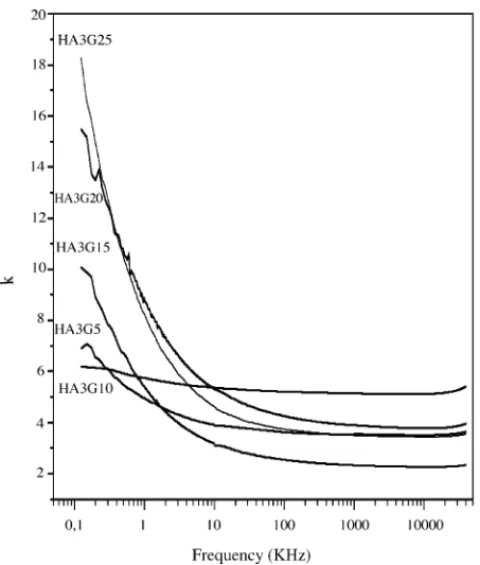
InFig. 9, one has the dielectric constant (DC) measure-ments of the films (seeTable 1). One can notice that, for all the films there is a decrease of the DC with the increase of the frequency. The DC was studied in the frequency range of 100 Hz–40 MHz (seeFigs. 11 and 12). At low frequency (1 kHz) the DC is lower for HA3G5 film (seeTable 1),K= 4.9 and increase slightly with the increase of the glass concentra-tion. For the film HA3G20 one hasK= 8.7. This is an interest-ing behavior that could be associated to the micro structural behavior of the film that was observed in the SEM analysis. In the presence of the glass, a spherical morphology for the synthesized particles in film HA3G5 was observed (Fig. 4). With the increase of the presence of the glass the grains are aggregating together forming plates for sample HA3G10 and HA3G20. This microstructural process seems to be very crit-ical in the electrcrit-ical properties of the films.
Fig. 11. Dielectric permittivity (K) as a function of frequency of the HA3GY series.
frequencies (1 MHz) the loss is lower, and for all films it is around (seeFig. 10) 10−2these values of DC and loss are
similar to those of Al2O3which is used conventionally for
microwave applications[26].
Fig. 12. Dielectric loss (D) as a function of frequency of the HA3GY series.
4. Conclusions
In this paper, we did a study on the structural and electrical properties of bioceramic hydroxiapatite (HA) thick films. The films were prepared in two layers using the screen-printing technique on Al2O3substrates. Mechanical alloying has been
used successfully to produce nanocrystalline powders of hy-droxyapatite (HA) to be used in the films. We also look for the effect of the grain size of the HA in the final properties of the film. The samples were studied using X-ray diffraction, scanning electron microscopy (SEM), electric and loss mea-surements, infrared and Raman scattering spectroscopy. We did a study of the dielectric permittivity and the loss of the films in the radio-frequency of the spectra.
The X-ray a diffraction (XRD) pattern of the films indi-cates that all the peaks associated to HA phase is present in the films. Extra peaks that are probably associated to the pres-ence of the flux material (powder glass) were observed. One can also notice an increase of the crystallite size to the firing process that the film was submitted. The crystallite size of the HA in the films are around 46 nm. The particle morphology of the films was investigated by means of SEM. The pres-ence of the glass is leading to a spherical morphology for the synthesized particles in the film. With the increase of the pres-ence of the glass the grains are aggregating together forming plates. The kind of grain clustering behavior will be very crit-ical in the electrcrit-ical properties of the films. Energy-dispersive spectroscopy analysis showed that the main elements of the HA film were carbon, oxygen, phosphorus and calcium. For the film with higher glass content it was observed, from the EDS analysis, that the Ca/P ratio around 2.3. The theoret-ical expected value for HA is around Ca/P = 2.15 which is reasonable agreement with the expected value. The infrared and Raman scattering spectroscopy results suggest that the firing process did not change much the optical properties of the thick films.
One can notice that, for all the films there is a decrease of the DC with the increase of the frequency. The values of the dielectric constant of the films are in between 4 and 9 (at 1 kHz), as a function of the flux concentration.
The loss is decreasing as we increase the frequency for all the films. The higher loss was observed for the high concen-tration of the flux material, withD= 0.7 at 1 kHz. The lower loss was obtained for low flux concentration (D= 0.1). For higher frequencies (1 MHz) the loss is lower, and for all films it is around 10−2. These values of DC and loss are similar to
those of Al2O3which is used conventionally for microwave
applications. This strongly suggests that the screen-printing HA thick films are good candidates for applications in bio-compatible coatings of implant materials.
Acknowledgements
References
[1] C. Lavernia, J.M. Schoenung, Bull. Am. Ceram. Soc. Ceram. Bull. 70 (1991) 95.
[2] V. Sergo, O. Sbaizero, D.R. Clarke, Biomaterials 18 (1997) 477. [3] B.R. Constantz, I.C. Ison, M.T. Fulmer, et al., Science 267 (1995)
1796.
[4] M.J. Yaszemsk, et al., Biomaterials 17 (1996) 175. [5] H.S. Liu, et al., Ceram. Int. 23 (1997) 19.
[6] G. Felicio Fernandes, et al., Quimica Nova 23 (2000) 441. [7] G. Heimke, Angew. Chem. 101 (1989) 111.
[8] L.L. Hench, J. Am. Ceram. Soc. 74 (1991) 1487. [9] M.R. Bet, et al., Quimica Nova 20 (1997) 475. [10] P. Ducheyne, et al., Biomaterials 11 (1990) 244. [11] M. Wei, et al., J. Biomed. Mater. Res. 45 (1999) 11.
[12] S. Ban, et al., Jpn. J. Appl. Phys. Part 2, Lett. 32 (10B) (1993) 1577. [13] C.M. Cotell, Appl. Surf. Sci. 69 (1993) 140.
[14] L. Torrisi, et al., Appl. Phys. Lett. 62 (1993) 237.
[15] L.D. Piveteau, et al., J. Mater. Sci. Mater. Med. 10 (1999) 161.
[16] T. Brendel, et al., J. Mater. Sci. Mater. Med. 3 (1992) 175. [17] E. Ruckenstein, et al., J. Colloid Interface Sci. 63 (1983) 245;
P. Baerti, et al., Appl. Surf. Sci. 54 (1992) 210. [18] C.M. Cotell, et al., J. Appl. Biomater. 3 (1992) 87. [19] R.K. Singh, et al., Biomaterials 15 (1993) 522.
[20] R.S. de Figueiredo, A. Messai, A.C. Hernandes, A.S.B. Sombra, J. Mater. Sci. Lett. 17 (1998) 449.
[21] I.F. Vasconcelos, et al., J. Mater. Sci. Lett. 18 (1999) 1871. [22] I.F. Vasconcelos, J. Mater. Sci. 36 (2001) 587.
[23] M.N. Taravel, Biomaterials 16 (11) (1995) 865–871. [24] S. Hontsu, et al., Thin Solid Films 295 (1997) 214.
[25] D.M. Liu, Q. Yang, T. Troczynski, Biomaterials 23 (2002) 691; Y. Mizutani, et al., J. Eur. Ceram. Soc.,www.sciencedirect.com, in press.
[26] A.J. Moulson, J.M. Herbert, Electroceramics, Chapman and Hall, 1990;