Gulrej Ahmed
1and Rajendra Kumar Baghel
2Department of Electronics and Communication Engineering, Maulana Azad National Institute of Technology (MANIT), Bhopal, India
A
BSTRACTThis paper presents the design of 6-bit flash analog to digital Converter (ADC) using the new variable switching voltage (VSV) comparator. In general, Flash ADCs attain the highest conversion speed at the cost of high power consumption. By using the new VSV comparator, the designed 6-bit Flash ADC exhibits significant improvement in terms of power and speed of previously reported Flash ADCs. The simulation result shows that the converter consumes peak power 2.1 mW from a 1.2 V supply and achieves the speed of 1 GHz in a 65nm standard CMOS process. The measurement of maximum differential and integral nonlinearities (DNL and INL) of the Flash ADC are 0.3 LSB and 0.6 LSB respectively.
K
EYWORDSVariable switching voltage, threshold inverter quantization, comparator, Flash ADC.
1. I
NTRODUCTIONAnalog-to-digital converter (ADC) has become essential structure for most of the electronics and communication systems. Comparator constitutes the main component in analog to digital conversion (ADC). It is basically the first stage in ADC, which converts the signal from analog to digital domain. The Flash ADC is the fastest ADC among all types of available ADC
architectures. An N-Bit Flash ADC employs the 2N-1 comparators for data conversion. However,
these comparators consume large power as they work simultaneously in parallel fashion. The Flash ADC also requires resistor ladder circuit or capacitor array circuit for reference voltage generation [2], which again makes the converter more power hungry & therefore Flash ADC consumes highest power among all types of ADCs. For low power data conversion circuits, the power dissipation has become one of the most important limitations. In reality, power efficiency has been considered as an essential design criterion in many battery employed applications such as wireless sensor node, pacemakers and other implanted RFID chips as biomedical imaging devices in the human body [4]. The objective in such cases is minimum power consumption for maximum battery life time. The designed 6-Bit Flash ADC in this paper meets the requirement for such low power applications.
2. R
ELATEDR
ESEARCHW
ORKresearch work under discussion contains only Flash ADC design using threshold voltage scaling of the comparator. In [5], a static inverter circuit has been explored as programmable logical buffer circuit and it has been suggested that the logic threshold voltage of CMOS inverter can be programmed to different specific logical voltages. These variable logical voltages can be evaluated mathematically. In [7], the thorough theoretical background of static CMOS inverter is elaborated. Using the aforementioned concept, a CMOS inverter has been realized as a threshold inverter quantization (TIQ) comparator [6]. The design of proposed TIQ comparator is a simpler as compared to traditional analog differential comparator. The basic thought is to simply apply the digital inverter as an analog voltage comparator. This also eliminates the resistive reference voltage circuit in Flash ADC. Thereby, static power consumption by resistive ladder circuit is removed. Inspired by the threshold voltage scaling, a reduced kickback comparator has been reported in literature [9]. Basically, it is a differential type of comparator, which can be designed with inbuilt threshold voltages. The design presented in [10] explored the TIQ comparator for 6-bit Flash ADC. It was basically implemented for system on chip (SOC) applications. The designed ADC was simpler and faster than other Flash ADCs. In this paper, the same research has been extended with the modified version of the comparator. The simulation results are better than the earlier reported works and the design 6-bit Flash ADC excels in terms of speed and power consumption.
3. C
OMPARATORThe function of a comparator is to generate an output voltage, which is high or low depending on whether the amplitude of the input is greater or lesser than a reference signal. It produces a binary output whose value is based on a comparison of two analog inputs. Typical comparators have differential type of architecture, and they can be further divided into open-loop and dynamic comparators. The open-loop comparators are fundamentally operational amplifier [4]. Dynamic comparators use positive feedback similar to flip-flops to accomplish the comparison of the magnitude between input and the external reference signal. However these differential types of comparator are intrinsically complex in design and consume high amount of power. On the other hand, single ended comparator architecture may be deployed as an analog comparator instead of using a whole analog block of comparator. The threshold inverter quantization (TIQ) comparators have been used to design the Flash ADC. The TIQ inverter based comparator consists of two cascaded inverters as shown in figure 1.
The inverter requires lesser number of transistors as compared to traditional comparator. In fact, a traditional comparator requires two input signal, while inverter based comparator requires only one input signal. The logic reference or switching voltage is generated by the inverter itself [5]. Graphically, the switching voltage can be identified at the intersection of the input voltage (Vin) and the output voltage (Vout) signal. At this point, both the transistor PMOS and NMOS are in the saturation region. By equating the drain current of devices, the switching threshold voltage can be determined. The mathematical formula for these switching voltages is given by the following equation [7].
= V − V k w w + V
kww + 1 1
Wherein, k denotes the mobility ratio of hole and electron, w & w are the channel width of PMOS (Mp1) & NMOS (Mn1) respectively, V & V are the threshold voltages of the devices Mn1 and Mp1 respectively. Further the equation can be simplified in terms of the channel width ratio of Mp1 and Mn1.
= V − V k w + V
k w + 1 2
Where, w is the ratio of channel width of devices Mp1 and Mn1. While driving the equation of
switching voltage, it has been assumed that both transistors PMOS & NMOS have the same channel length. The logic threshold voltage of a CMOS inverter is determined by the channel
width ratio W of the PMOS and NMOS transistors. However at 65nm standard CMOS process,
the switching voltage is not governed by the equation (2), it is due to the fact that short channel devices do not follow the square law relation and in such case, the switching voltage is controlled by effective resistance of the devices [8], it is therefore given by following equation.
= r r+ r 3
Where r and r are the effective switching resistances of NMOS (Mn1) and PMOS (Mp1)
transistors of the first stage inverter at channel length (L) =65nm, respectively. The resistance
r and r are the function aspect ratio (W/L) of the devices, thus the switching voltages can be programmed to specific values by varying the aspect ratio.
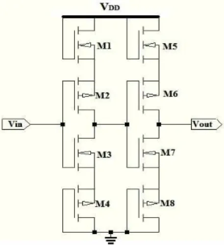
3.1. VARIABLE SWITCHING VOLTAGE COMPARATOR
Figure 2. Proposed VSV Comparator
This causes reduction in the drain current of Mn1 and Mp1 of the first stage. This in turn decreases the power consumption of the first stage. The same remark is applied to the second stage of the comparator. In fact, the second stage provides sharper switching of the logical voltages and it is used to invert the output of the first stage. Note that the devices M1, M4, M5 and M8 are always in saturation because drain and gate terminals are at the same potential i.e. VG=VD. The saturated device offers an active resistance, which can be determined by its transconductance ($%).For the NMOS device, it is given by the following equation.
$%=&&'
( = )2 *
+
,-./. 012I 4
This can be further simplified in terms of the aspect ratio (56.) and process transconductance (7.8) of NMOS device.
$%= 256.7.8I 5
Similarly for the PMOS device, the transconductance ($%) may be given as.
$%= 256:7:8' 6
The switching voltage of first stage of the proposed comparator can be evaluated in the same manner as in equation 3.
= 1 r <+ 1g > g + r ?+ r <+ 1g >
Comparator
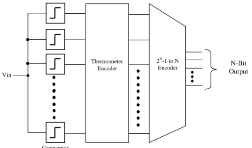
Vin
Thermometer Encoder
2N-1 to N
Encoder N-Bit
Output Where 1Ag & 1Ag > are the active resistance of M1 and M4 respectively, while r ? & r < are the effective switching resistances of M2 and M3 transistors. Since the switching resistance of a transistor depends on its channel width, therefore the width of the devices M1, M2 and M3, M4 is varied to obtain the 63 different switching voltages as shown in figure 3.
Figure 3. Switching voltages of 6-bit Flash ADC
Using the proposed comparator, a low-power 6-bit Flash ADC is designed and simulated. A comparative analysis is also presented to justify the power reduction in the proposed comparator.
3.2 FlashADC
The generalized block diagram of N-bit Flash ADC is shown in the figure 4. A 6-bit Flash ADC requires 63 numbers of comparator at the input side of the block diagram. An analog input voltage (Vin) goes through each comparator, the comparators compare the input voltage with internal reference voltages, which are determined by the aspect ratio of CMOS transistors of VSV Comparator. These comparators work simultaneously. The comparator’s output will be either ‘1’ or ‘0’ depending on internal reference voltage of the comparator.
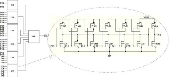
For 6-bit Flash ADC, the digital switching signals (thermometer codes) are produced by the array of 63 comparators. The thermometer codes are converted into intermediate codes to minimize the bubble error in the code. The output of the thermometer encoder is shown in figure 6.
Figure 5. Second Stage Encoder
Figure 6. Waveform of 63 Intermediate codes
The intermediate codes are fed to 2N-1 to N encoder block. The encoder performs second step of
encoding as shown in figure 5. Basically, it encodes the single bit. There are as such 6 encoder blocks associated with each bit for performing the encoding process. Table 1 summarizes this final encoding process for all 6-bits.
Table 1. Encoder Input Combinations
Encoder Input Encoder Output
E5 E4 E3 E2 E1 E0
P5 I37 I21 I13 I13 I11 I11 P6 I38 I22 I14 I14 I14 I13 P7 I39 I23 I15 I15 I15 I15 P8 I40 I24 I24 I20 I18 I17 P9 I41 I25 I25 I21 I19 I19 P10 I42 I26 I26 I22 I22 I21 P11 I43 I27 I27 I23 I23 I23 P12 I44 I28 I28 I28 I26 I25 P13 I45 I29 I29 I29 I27 I27 P14 I46 I30 I30 I30 I30 I29 P15 I47 I31 I31 I31 I31 I31 P16 I48 I48 I40 I36 I34 I33 P17 I49 I49 I41 I37 I35 I35 P18 I50 I50 I42 I38 I38 I37 P19 I51 I51 I43 I39 I39 I39 P20 I52 I52 I44 I44 I42 I41 P21 I53 I53 I45 I45 I43 I43 P22 I54 I54 I46 I46 I46 I45 P23 I55 I55 I47 I47 I47 I47 P24 I56 I56 I56 I52 I50 I49 P25 I57 I57 I57 I53 I51 I51 P26 I58 I58 I58 I54 I54 I53 P27 I59 I59 I59 I55 I55 I55 P28 I60 I60 I60 I60 I58 I57 P29 I61 I61 I61 I61 I59 I59 P30 I62 I62 I62 I62 I62 I61 P31 I63 I63 I63 I63 I63 I63
In the conventional Flash ADC, all the comparators are identical and reference voltages are generated by resistor ladder circuit. On the other hand, In the VSV comparator based Flash ADC, the desired internal reference voltage is generated by comparator itself just like TIQ comparator based Flash ADC. Therefore 2N-1 different sizes of comparators are needed for generation of 2N-1 reference voltages and resistor ladder network is not required for the external reference voltage generation.
4. R
ESULTS& D
ISCUSSIONFigure 7. Power comparison of VTV comparator & TIQ comparator
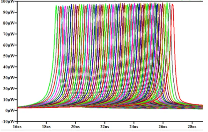
The comparison of power consumption between TIQ comparator and proposed VSV comparator is shown in figure 7. For 6-bit Flash ADC, the power consumption of TIQ comparator array and proposed VSV comparator array are shown in figure 9 and 10 respectively.
Figure 8. Power consumption of TIQ comparators array
Using the proposed comparator, a 6-Bit Flash ADC has been designed and simulated at 65nm standard CMOS process. The design is simpler than the conventional Flash ADC and it does not require the resistive ladder for reference voltage generation.
Figure 10. Transient analysis of the 6-bit Flash ADC
The transient analysis of the ADC is made by giving a ramp input signal ranging from 562mV to 680 mV and each LSB voltage level is of 2.1mV. The digital codes are obtained correctly for 6-bit ADC as shown in figure 10. The plot of the measured differential nonlinearity (DNL) for the designed ADC is shown in figure 11.
Figure 11.Measurement of DNL of the 6-Bit Flash ADC
The measurement of integral nonlinearity (INL) is drawn in the figure 12. It is clear from the plot that, the measured INL is lesser than 0.6 LSB. This shows functional correctness of the designed 6-bit Flash ADC
Table 2. Comparison Summary of Simulation Results
Parameter Proposed
work Reported work [1] Reported work [2] Reported work [3] Reported work [10]
Resolution 6-bit 6-bit 6-bit 6-bit 6-bit
Architecture Flash Flash Flash Flash Flash
Technology 65 nm 90 nm 130 nm 65 nm 250 nm
DNL (LSB) 0.3 0.5 0.4 0.5 --
INL (LSB) 0.6 0.96 0.6 0.5 --
Voltage Supply 1.2 V 0.9 V 1.2 V 1.2 V 2.5 V
Power Dissipation 2.1 mW 98 mW 90 mW 12 mW 66.8 mW
Samples/sec. 1G 3.5G 600M 800M 1G
Ladder Network No Yes Yes Yes No
The different parameters obtained for 6-bit Flash ADC are compared with earlier reported work in Table 2. For transparent comparison, only Flash ADC architectures of 6-bit resolution have been selected. It can be observed from the above table that the proposed comparator based Flash ADC consume the lowest power at the speed of 1 GHz. The measured DNL and INL are also lesser than 1 LSB. This guarantees that, the designed 6-bit flash ADC is monotonic in nature.
5. C
ONCLUSIONA 6-bit Flash ADC has been designed by employing the proposed VSV comparator. The design has been carried out in digital 65nm standard CMOS technology. Further lower feature size and smaller supply voltage can be incorporated in the design. At 1 GHz speed, the Flash ADC dissipates peak power of 2.1mW and average power of only 244 W. The measured maximum differential and integral nonlinearities (DNL and INL) for a ramp input are found to be 0.3 LSB & 0.6 LSB respectively. The parameters DNL & INL are improved as compared to earlier reported works. The designed 6-bit Flash ADC exhibits significant improvement in terms of power and speed of previously reported Flash ADCs. This makes it highly suitable ADC for high speed and low power application.
R
EFERENCES[1] Deguchi, K., Suwa, N., Ito, M., Kumamoto, T., & Miki, T. (2008) “A 6-bit 3.5-GS/s 0.9-V 98-mW flash ADC in 90-nm CMOS. IEEE Journal of Solid-State Circuits”, Vol. 43, No. 10, pp2303-2310.
[2] Kuttner, A. S. T. H. F., Sandner, C., & Clara, M. (2005) “A 6bit, 1.2 gsps low-power flash-adc in 0.13 µm digital cmos”, IEEE Journal of Solid-State Circuits Vol. 40, No.7.
[3] Chen, C. Y., Le, M. Q., & Kim, K. Y. (2009) “A low power 6-bit flash ADC with reference voltage and common-mode calibration”, IEEE Journal of Solid-State Circuits, Vol. 44, No. 4, pp1041-1046.
[5] Segura, J., Rossello, J. L., Morra, J., & Sigg, H. (1998) “A variable threshold voltage inverter for CMOS programmable logic circuits”, IEEE Journal of Solid-State Circuits, Vol. 33, No.8, pp1262-1265.
[6] Tangel, A., & Choi, K. (2004) “The CMOS Inverter as a comparator in ADC designs”, Analog Integrated Circuits and Signal Processing, Vol. 39, No.2, pp147-155.
[7] Rabaey, J. M., Chandrakasan, A. and Nikolic , B. (2003) “Digital Integrated Circuits”, 2nd Edition. [8] Baker, R. J. (2005) “CMOS: Circuit Design, Layout and Simulation”, IEEE Press Wiley India
Edition.
[9] Torfs, G., Li, Z., Bauwelinck, J., Yin, X., Van der Plas, G., & Vandewege, J. (2011) “ Low-power 4-bit flash analogue to digital converter for ranging applications”, Electronics letters, Vol. 47, No.1, pp 20-22.
[10] Yoo, J., Choi, K., & Tangel, A. (2001). “A 1-GSPS CMOS flash A/D converter for system-on-chip applications”, In Proceedings of IEEE Computer Society Workshop on VLSI, pp. 135-139.
[11] Nuzzo, P., Van der Plas, G., De Bernardinis, F., Van der Perre, L., Gyselinckx, B., & Terreni, P. (2006) “ A 10.6 mW/0.8 pJ power-scalable 1GS/s 4b ADC in 0.18 m CMOS with 5.8 GHz ERBW”, In Proceedings of the 43rd annual Design Automation Conference ,pp. 873-878.
[12] Park, S., Palaskas, Y., & Flynn, M. P. (2007) “A 4-GS/s 4-bit flash ADC in 0.18- m CMOS”, IEEE Journal of solid-State Circuits, IEEE Journal of Vol. 42, No.9, pp1865-1872.
[13] Sundström, T., & Alvandpour, A. (2010) “A 6-bit 2.5-GS/s flash ADC using comparator redundancy for low power in 90 nm CMOS”, Analog Integrated Circuits and Signal Processing, Vol. 64, No.3, pp215-222.
[14] Van der Plas, G., Decoutere, S. & Donnay, S. (2006) “A 0.16 pJ/conversion-step 2.5 mW 1.25 GS/s 4b ADC in a 90nm digital CMOS process”, IEEE International Solid-State Circuits, Digest of Technical Papers, p. 2310.
[15] Choi, M., & Abidi, A. A. (2001) “A 6-b 1.3-Gsample/s A/D converter in 0.35- m CMOS”, IEEE Journal of Solid-State Circuits, vol. 36, no. 12, pp. 1847-1858.
AUTHORS
Gulrej Ahmed has received his B.E. (Electronics and Instrumentation Engineering) in 2001 from the SGSITS, Indore, India. He has received M. E. (Digital Communication) in 2006 from I.E.T. DAVV, Indore. He is currently pursuing PhD from MANIT, Bhopal, India. His research interest includes Low Power Design of VLSI circuits, Data Converters and Mixed Signal Design.
![Figure 1. TIQ Comparator [6]](https://thumb-eu.123doks.com/thumbv2/123dok_br/17166091.240991/2.918.318.583.749.992/figure-tiq-comparator.webp)

![Table 2. Comparison Summary of Simulation Results Parameter Proposed work Reported work [1] Reported work [2] Reported work [3] Reported work [10]](https://thumb-eu.123doks.com/thumbv2/123dok_br/17166091.240991/10.918.186.741.223.545/comparison-simulation-parameter-proposed-reported-reported-reported-reported.webp)
