APPLICATION NOTE
DESIGN NOTES ON PRECISION PHASE LOCKED SPEED
CONTROL FOR DC MOTORS
ABSTRACT
There are a number of high volume applications for DC motors that require precision control of the motor’s speed. Phase locked loop techniques are well suited to provide this control by phase locking the motor to a stable and accurate reference frequency. In this paper, the small sig-nal characteristics, and several large sigsig-nal effects, of these loops are considered. Models are given for the loop with design equations for determining loop bandwidth and stability. Both voltage and current motor drive schemes are addressed. The design of a loop for a three phase brushless motor is presented.
PHASE LOCKING GIVES PRECISION SPEED
CONTROL
The precise control of motor speed is a critical function in today’s disc drives. Other data storage equipment, includ-ing 9 track tape drives, precision recordinclud-ing equipment, and optical disc systems also require motor speed control. As the storage density requirements increase for these media, so does the precision required in controlling the speed of the media past the read/write mechanism. One of the best methods for achieving speed control of a mo-tor is to employ a phase locked loop.
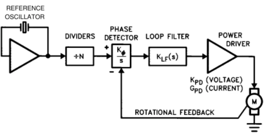
With a phase locked loop, a motor’s speed is controlled by forcing it to track a reference frequency. The reference input to the phase locked loop can be derived from a pre-cision crystal controlled source, or any frequency source with the required stability and accuracy. A block diagram of the phase locked loop is shown in Figure 1.
REFERENCE OSCILLATOR
In Figure 1, a precision crystal oscillator’s frequency is digitally divided down to provide a fixed reference frequen-cy. Alternatively, the motor could be forced to track a vari-able frequency source with zero frequency error. The mo-tor speed is sensed by either a separate speed winding or, particularly in the case of the DC brushless motor, a Hall effect device. The two signals, motor speed and ref-erence frequency, are inputs to a phase detector. The de-tector output is a voltage signal that is a function of the phase error between the two inputs. The transfer function of the phase detector, K+, is expressed in volts/radian. A 1/s multiplier accounts for the conversion of frequency to phase, since phase is the time integral of frequency.
Following the phase detector is the loop filter. This block contains the required gain and filtering to set the loop’s overall bandwidth and meet the necessary stability criteria. The output of the loop filter is the control input to the mo-tor drive. Depending on the type of drive used, voltage or current, the driver will have respectively, a VOUT/VIN transfer characteristic, or an louT/Vr~ transconductance.
At first glance, it seems that the motor has simply re-placed the VCO (voltage controlled oscillator), in the clas-sic phase locked loop. In fact, it is a little more complicat-ed. The mechanical and electrical time constants of the motor come into play, making the transfer function of the motor more than just a voltage-in, frequency-out block. In order to analyze the loop’s small and large signal behav-ior it is essential to have an equivalent electrical model for the motor.
A SIMPLE ELECTRICAL MODEL FOR A DC
MOTOR
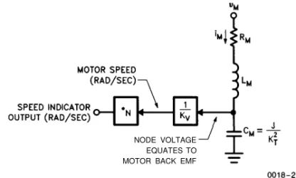
Figure 2 is an electrical representation of a DC motor. The terms used are defined here:
LM Motor winding inductance in henrys HM Motor winding resistance in as
J Total moment of inertia of the motor in Nm-set? (Note: 1 Nm = 141.6 oz-in)
KT Motor torque constant in Nm/Amp
Kv Voltage constant (back EMF) of motor in voltage-sec/rad
Figure 1. Precise motor speed control is obtained by phase locking
NODE VOLTAGE EQUATES TO MOTOR BACK EMF
*N = Number of speed sense cycles per motor revolution
Figure 2. This simple electrical model is useful for determining the small and large signal characteristics of the motor. Capacitor, CM is used to model the mechanical energy storage of the motor.
In this model the winding inductance and resistance ele-ments correlate directly with the corresponding physical parameters of the motor, with values taken directly off the manufacturer’s data sheet. The capacitor, CM, models the mechanical energy storage of the motor. Current into the capacitor equates, via motor constant KT, to motor torque, and the voltage across the capacitor is equal to the motor back EMF. The back EMF voltage equates to motor ve-locity through the inverse of Kv. In the model, the term N is simply a multiplier equal to the number of feedback cy-cles obtained per revolution of the motor. For example, in a 4 pole brushless DC motor the commutation Hall effect device outputs will be at twice the rotational frequency of the motor, making N equal to 2.
The equation for the capacitor, given in Figure 2, has the units of Farads if J and KT are expressed in SI units. In modeling the overall transfer characteristic, it is important that the moment of inertia of the load on the motor be added to the moment of inertia of the motor itself.
It is worthwhile to note that the current into the motor, mi-nus idling current, is proportional to acceleration of the motor. This is easily seen from the model by realizing that the time derivative of the capacitor voltage relates directly to acceleration. The effects of loads on the motor can be modeled by including a current source across the capaci-tor for constant capaci-torque loads, or a resiscapaci-tor for loads that are linearly proportional to motor speed.
TRANSFER FUNCTIONS FOR VOLTAGE AND
CURRENT DRIVEN MOTORS
Using the electrical model, the small signal transfer func-tion of the motor is easily derived. Equafunc-tions 1a and 1b give the small signal frequency response for both the cur-rent and voltage driven cases respectively.
The transfer function given in equation (1a) describes the small signal response of motor speed, OM(s), to changes in the drive current. Equation (1b) relates the dependence of motor speed to motor drive voltage.
The small signal response of the motor for the current driven case has a DC pole that results from the relation-ship of motor torque to velocity, that is, motor velocity is proportional to the integral of motor torque over time. In the current driven motor neither the winding resistance nor inductance appear in the transfer function. This is be-cause these elements are in series with the current source output of the driver stage. As long as the output impedance of the driver remains large relative to the im-pedance of these elements, the resistance and induc-tance of the motor will have a negligible effect on the small signal response.
The voltage driven response has a second order charac-teristic that results from the interaction of the series RLC. In many cases the transfer function of the voltage driven case can be simplified. If the quality factor of the series RLC of the motor model is much less than one, as de-fined in equation 2, then the response of the motor can be accurately approximated by equation 3.
CONSIDERING THE WHOLE LOOP
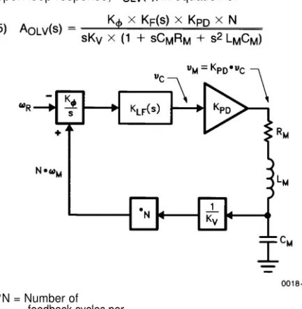
Figure 3 shows the complete speed control loop for the current driven case. The overall open loop response, AoLc, is easily written.
“N = Number of feedback cycles per motor revolution
Figure 3. In this phase locked loop, with current mode drive to the motor, the motor winding resistance and inductance can be ignored as long as the current driver maintains a high output impedance.
(5)
For this loop, note that there are two poles in the re- For this motor, the model capacitor, CM, is calculated us-sponse at DC, i.e., s = 0. One pole is due to the reus-sponse ing the equation in Figure 2 to be equal to 4.4 Farads. If of the current driven motor, the second pole is from the we calculate the quality factor of the series RLC, using frequency to phase transformation of the phase detector. equation 2, we find it is equal to 42.4 x 10 -3. This is The 180 degrees of phase shift this pair of poles intro- considerably less than one, and the response closely ap-duce force a phase lead configuration of the loop filter in proximates the non-complex response of equation 3 with order to obtain a loop phase margin greater than zero. poles at 0.014 Hz and 199 Hz.
The complete voltage loop is shown in Figure 4, and its open loop response, AoLv(s), in equation 5.
Typical loop bandwidths will fall well inside this range of frequencies. As long as this is true, the loop response with a voltage driven motor can be approximated by:
This expression is the same as the current driven re-response equation 4, with the transconductance of the cur-rent drive stage, GPD, replaced by the gain of the voltage
drive stage divided by the motor winding resistance,
*N = Number of
feedback cycles per motor revolution
Figure 4. With voltage mode drive to the motor the electrical time constant of the motor plays a part in the small signal response of the speed control loop.
This response has only one pole at DC, although the total number of poles is three versus two for the current driven case. For most motors, particularly those used in constant velocity applications, this transfer function can be simpli-fied by applying the results of equations 2 and 3. This is best illustrated by looking at an example. Consider the fol-lowing motor, (typical 3-phase brushless for disc drive ap-plications):
KT . . . .1.5 X 10-Z Nm/Amp Kv . . . .1.5 X 10-Z V-sec/rad J (including platters) . . . 1 X 10-s Nm-sec2 RM . . . ..2.5R
LM 2mH
CLOSING THE LOOP
When it comes to closing the loop the goal is to have a stable loop with the required loop bandwidth. The vari-ables that must be considered are:
1) The motor
2) The power driver, type and gain 3) The phase detector gain 4) Loop bandwidth
5) The loop filter
The first four of the above variables are usually dictated by conditions other than the stabilizing of the loop. This leaves the loop filter as the tool for achieving the small signal loop requirements.
NORMALIZED FREQUENCY
0018-5
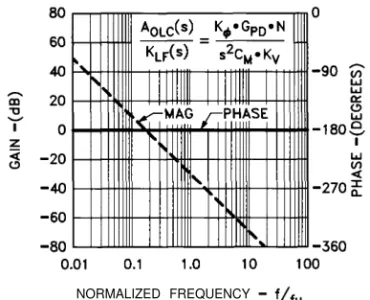
Figure 5. A Bode plot of the combined gain and phase response of the motor, motor drive, and phase detector is useful in determining the requirements on the loop filter. This plot is normalized to the desired open loop unity gain frequency.
From Figure 5 two restrictions on the loop filter are readily apparent. First, since the remaining portion of the loop has 180° of phase shift over the entire frequency range, the loop filter must have a phase lead at the unity gain frequency and at all frequencies below the unity gain fre-quency. By meeting this restriction the small signal loop will be unconditionally stable.
Secondly, in order to achieve the desired loop bandwidth, the loop filter must have a voltage gain at the desired uni-ty gain frequency of 30 dB. This level is simply the inverse of the remaining loop’s voltage gain at the unity gain fre-quency.
A loop filter configuration that will meet these restrictions is shown in Figure 6. Also shown in this figure is the small signal response equation for the filter. The response starts out from DC with a flat inverting gain that breaks upward at the zero frequency, OZ, and then flattens out again at the pole, op. The pole in this response is neces-sary to prevent excess feedthrough of residual reference frequency that is present at the outputs of many digital type phase detectors–in fact, as will be discussed in the design example, a separate reference filter is normally re-quired.
A good choice for the relative positioning of the pole and zero of the loop filter response is to space them apart by 1 decade of frequency, and center them around the unity gain frequency. Figure 7 shows the Bode plots of this sug-gested positioning applied to the case illustrated in Figure 5. As shown, a phase margin of about 45° is obtained with this configuration.
Figure 6. This loop filter configuration provides the required phase lead and gain at the loop crossover frequency.
0.01 0.1 1.0 10 100
NORMALIZED FREQUENCY - f/f”
0 0 1 8 - 7 Figure 7. Using the criteria set forth for the design of the loop
filter, the resulting Bode plot indicates a phase margin of 45°.
If the above results are acceptable, then the following simple steps can be applied to pick the loop amplifier component values. Referring to Figure 6.
1) Pick R3 to be as high in value as acceptable for the Op-Amp and board restrictions.
2) Rt = (R3 x 3.33)/10x/*0, where X is the voltage gain, in dB, required at the unity gain frequency.
3) R2 = RI/~, sets a 10:1 ratio for op to OZ.
4) Cl = (277 x R2 x 3.33 x f,) - 1, where f, is the loop unity gain frequency.
Using this simple procedure the small signal loop is easily closed for stable static operation.
A DESIGN EXAMPLE
As an example, let us take a look at the complete design of a constant velocity speed control loop for a disc drive application. The performance characteristics for the circuit can be summarized as:
Motor speed . . . 3600 rpm ± 60 ppm (0.006%) Speed stability . . . .± 50 ppm Start-up lock time . . . 10 seconds Input voltage . . . .12 Volts Motor idling current . . . .0.5 Amps
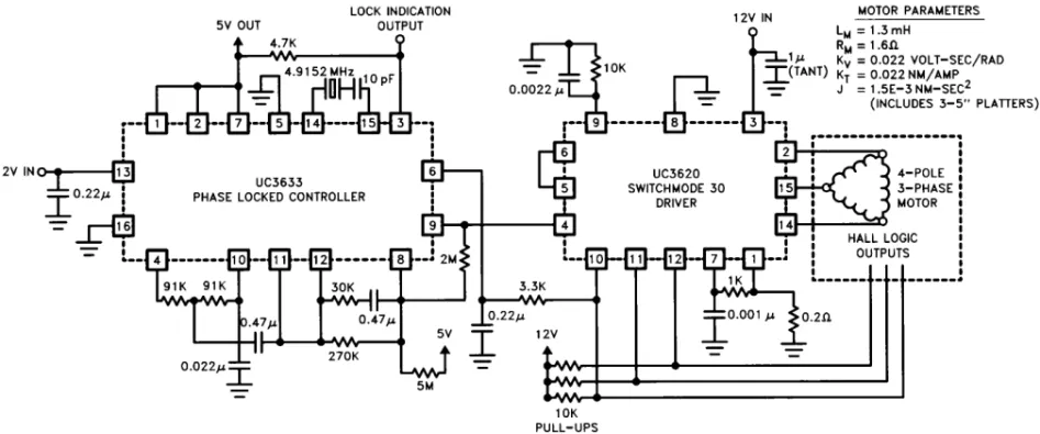
The schematic for this design is shown in Figure 8. The motor is a 4 pole 3-phase brushless with the electrical and mechanical specifications given in the figure. The mo-tor is current mode driven with the UC3620 3-phase Switchmode Driver. The speed control function is realized with the UC3633 Phase Locked Controller.
0 0 1 8 - 8
POWER DRIVER STAGE
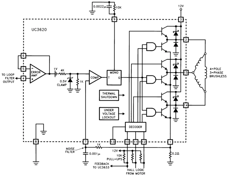
a chopping frequency of well over 20 kHz under normal operating conditions.In Figure 9 a detail of the driver IC and the associated cir-cuitry is shown. The UC3620 is a current-mode, fixed off-time, chopper. Three 2-Amp totem pole output stages with catch diodes drive the three motor phases. The outputs are enabled by the internal commutation logic that re-sponds to the three Hall logic signals from the motor. The motor is equipped with open collector Hall devices making the three 10k pull-up resistors on the UC3620 Hall inputs necessary.
Current is controlled by chopping the lowside drive to the phase winding under the command of the UC3620’s cur-rent sense comparator. The RC combination on the timing pin of the driver sets the off-time at 22 ps. This results in
The transconductance of the driver is set by the value of current sense resistor used at the emitter pin of the UC3620. With a value of 0.2R the transconductance from the error amplifier output to the driver outputs is 1 Amp/ Volt. The UC3620 error amplifier is configured here as a unity gain buffer, thus the drive control signal is applied at the non-inverting error amplifier input with the same over-all transconductance. An internal 0.5V clamp diode at the current sense comparator input results in a 2.5 Amp maxi-mum drive current. There is a 1V offset internal to the UC3620 that is reflected to the drive control input at zero current. This offset combines with the 0.5 Amp idling cur-rent level of the motor to set the steady state DC voltage at the driver control input to be 1.5V.
Figure 10. Phase locking the motor to a precision reference frequency is achieved with the UC3633. The double edge sensing option on this device doubles the loop gain and allows twice the reference frequency to be used for a given motor RPM by forcing the phase detector to respond to both edges of the Hall feedback signal.
PHASE LOCKED CONTROL CIRCUIT
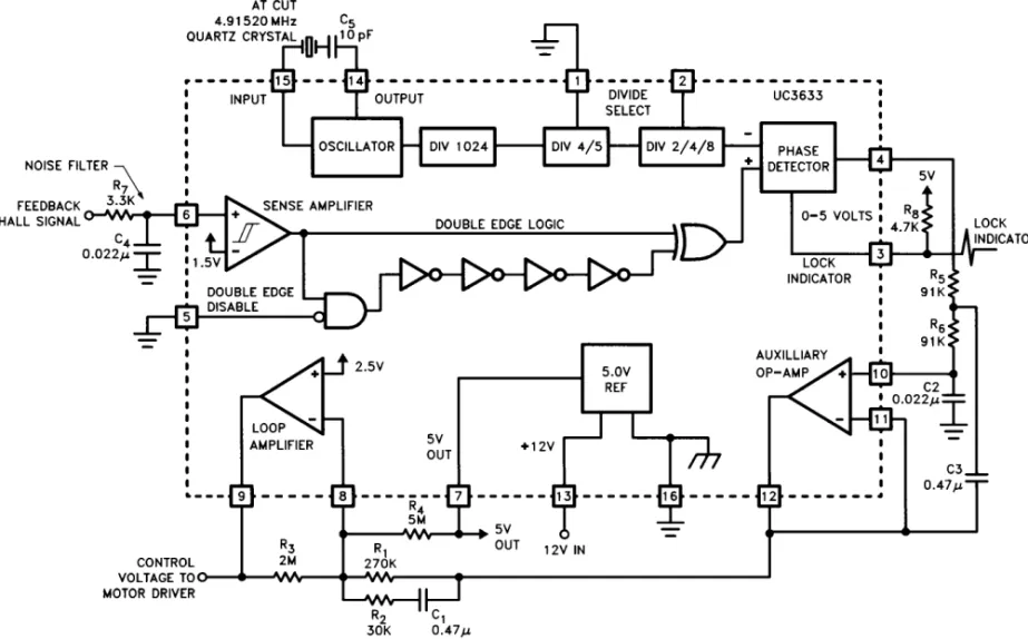
A detail of the phase locked control portion of the design is given in Figure 10. The UC3633 contains all of the cir-cuitry required for this function including: a crystal oscilla-tor, programmable reference dividers, a digital phase de-tector, and op-amps for the required filtering. The UC3633 receives velocity feedback from the Hall signal applied at its sense amplifier input pin. The sense amplifier has a small amount of hysteresis that provides fast rising and falling input edges to the following logic. A double edge option is available on the UC3633 sense amplifier. When this option is enabled, as it is in this design, the phase de-tector is supplied with a short pulse on both the rising and falling edges of the feedback signal, effectively doubling the loop gain and reference frequency.
The required reference frequency for this loop is 240 Hz, given by the product of the motor rotation of 3600 rpm (60 Hz), the number of cycles/revolution at the Hall out-puts (two for a 4 pole motor), and a factor of two as a result of the double edge sensing. The divider options on the UC3633 are set up such that standard microprocessor crystals can be used. In this instance, a 4.91520 MHz ( ± 50 ppm) AT cut crystal is divided by 20,480 to realize a 240 Hz reference frequency input to the phase detector.
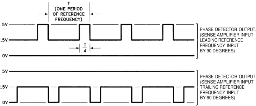
PHASE DETECTOR OUTPUT, (SENSE AMPLIFIER INPUT LEADING REFERENCE FREQUENCY INPUT BY 90 DEGREES)
PHASE DETECTOR OUTPUT, (SENSE AMPLIFIER INPUT TRAILING REFERENCE FREQUENCY INPUT BY 90 DEGREES)
0 0 1 8 - 1 1 Figure 11. The phase detector on the UC3633 is a digital circuit that responds to phase error with a pulsed output at the reference frequency
rate. The width and polarity of the pulses depend respectively on the phase error magnitude and polarity. If any static frequency error is present, the detector will respond with a constant 0 Volt or 5 Volt signal depending on the sign of the error present.
The pulses are always 2.5V in magnitude and are refer-enced to 2.5V at the detector output. The polarity of the output pulses tracks the polarity of the input phase error. This operation is illustrated in Figure 11. The resulting phase gain of the detector is 2.5V/2~ radians, or about 0.4V/rad, with a dynamic range of f 2~ radians.
The phase detector also has the feature of absolute fre-quency steering. If any static frefre-quency error exists be-tween the two inputs, the output of the detector will stay in a constant high, or low state; 5V, if the feedback input rate is greater than the reference frequency and 0V, if the opposite frequency relationship exists. The lock indicator output on the UC3633 provides a logic low output when any static error exists between the feedback and refer-ence frequencies.
A unity gain bandwidth of 4 Hz was chosen for this loop. This unity gain frequency is well below the effective sam-pling frequency, the 240 Hz reference, and is sufficiently high to not significantly affect the start-up lock time of the drive system. The design of the loop filter follows the guidelines described earlier. The magnitude of the loop gain, minus the loop filter, at 4 Hz is equal to:
This dictates that the loop amplifier has a gain of 28.6 dB at 4 Hz. A value for the loop amplifier feedback resistor, Rs, of 2 MR was chosen. The values for RI, R2 and Cl were calculated as follows.
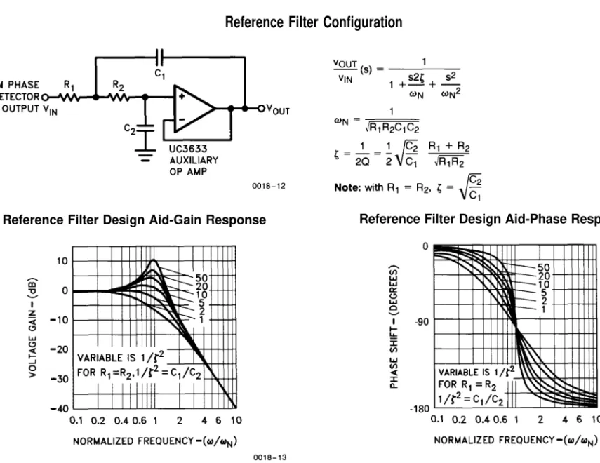
The additional op-amp on the UC3633 is used to realize a second order active filter to attenuate the reference com-ponent out of the phase detector. The filter is a standard quadratic with a natural frequency of 17.2 Hz and a Q of about 2.3. This circuit provides 46 dB of attenuation at 240 Hz while adding only 5° of phase shift at the 4 Hz loop crossover frequency. In Figure 12 design guidelines and response curves for this filter are given.
Reference Filter Configuration
Reference Filter Design Aid-Gain Response Reference Filter Design Aid-Phase Response
Figure 12. To keep feedthrough of the residual reference frequency at the phase detector output to a minimum, a simple quadratic filter can be used. The design of this filter is easily accomplished with the above equations and response curves.
As mentioned earlier, a separate reference filter is re-quired in this type of phase locked loop to attenuate the reference frequency feedthrough at the output of the phase detector. With the active filter following the phase detector, the feedthrough to the loop amplifier is kept to less than 20mV,, under the worst case condition of f ~(180”) phase error. This is small compared to the 1.25V DC signal out of the detector at this phase error. If the reference ripple into the loop amplifier becomes large compared to the averaged phase error term, large signal instabilities may result. These are primarily the result of the unidirectional nature of the motor drive.
the 5V reference sets the zero phase operating voltage at the loop filter output to 1.5V. This matches the nominal operating voltage required at the UC3620 control input, taking into account the 0.5 Amp idling current of the mo-tor and the 1V offset of the driver. This cancellation is subject to variations due to shifts in DC operating levels, so, while it does significantly reduce static reference feed-through, it can not be expected to reliably set exactly zero phase operation.
The oscilliscope traces in Figure 13 show the Hall input to the UC3633 along with the output waveform of the digital phase detector under static phase locked conditions. No-tice that the phase detector output is alternating between positive and negative output pulses. This is a result of a slight asymmetry on the Hall input signal in conjunction with the use of the double edge sensing being used. In
this case, the asymmetry is due to differences in the rising and falling edges of the Hall signal that result from the RC filter at the sense amplifier input. This filter is required to keep high frequency noise from the motor drive out of the phase detector.
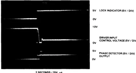
The startup response of the motor is pictured in Figure 14. Shown are the voltage waveforms at the lock indicator output, the loop amplifier output, and the phase detector output of the UC3633. At the moment the lock indicator goes high the motor has reached its operating velocity. The absolute frequency steering of the phase detector forces a slight overshoot in frequency that delays the set-tling of the loop by about 1 second. Without the frequency steering feature the phase detector would command a much lower average drive signal during startup, extending the start time by over 50%.
0 0 1 6 - 1 5
Figure 13. This oscilloscope trace shows the static waveforms at the Hall sensor input, and phase detector output of the UC3633. The static phase error has been adjusted, with R4 in Figure 10, to be very small. The alternating positive and negative pulses at the output of the phase detector is due to an asymmetry in the Hall signal.
0 0 1 8 - 1 6
Figure 14. The startup lock time of the motor is minimized with the absolute frequency steering feature of the phase detector, keeping lock times under 10 seconds.
Unitrode Corporation makes no representation that the use or interconnection of the circuits described herein will not in-fringe on existing or future patent rights, nor do the descriptions contained herein imply the granting of licenses to make, use or sell equipment constructed in accordance therewith.
© 1987 by Unitrode Corporation. All rights reserved. This bulletin, or any part or parts thereof, must not be reproduced in any form without permission of the copyright owner.
NOTE: The information presented in this bulletin is believed to be accurate and reliable. However, no responsibility is as-sumed by Unitrode Corporation for its use.
any product or service without notice, and advise customers to obtain the latest version of relevant information to verify, before placing orders, that information being relied on is current and complete. All products are sold subject to the terms and conditions of sale supplied at the time of order acknowledgement, including those pertaining to warranty, patent infringement, and limitation of liability.
TI warrants performance of its semiconductor products to the specifications applicable at the time of sale in accordance with TI’s standard warranty. Testing and other quality control techniques are utilized to the extent TI deems necessary to support this warranty. Specific testing of all parameters of each device is not necessarily performed, except those mandated by government requirements.
CERTAIN APPLICATIONS USING SEMICONDUCTOR PRODUCTS MAY INVOLVE POTENTIAL RISKS OF DEATH, PERSONAL INJURY, OR SEVERE PROPERTY OR ENVIRONMENTAL DAMAGE (“CRITICAL APPLICATIONS”). TI SEMICONDUCTOR PRODUCTS ARE NOT DESIGNED, AUTHORIZED, OR WARRANTED TO BE SUITABLE FOR USE IN LIFE-SUPPORT DEVICES OR SYSTEMS OR OTHER CRITICAL APPLICATIONS. INCLUSION OF TI PRODUCTS IN SUCH APPLICATIONS IS UNDERSTOOD TO BE FULLY AT THE CUSTOMER’S RISK.
In order to minimize risks associated with the customer’s applications, adequate design and operating safeguards must be provided by the customer to minimize inherent or procedural hazards.
TI assumes no liability for applications assistance or customer product design. TI does not warrant or represent that any license, either express or implied, is granted under any patent right, copyright, mask work right, or other intellectual property right of TI covering or relating to any combination, machine, or process in which such semiconductor products or services might be or are used. TI’s publication of information regarding any third party’s products or services does not constitute TI’s approval, warranty or endorsement thereof.