Article
J. Braz. Chem. Soc., Vol. 26, No. 12, 2545-2557, 2015. Printed in Brazil - ©2015 Sociedade Brasileira de Química 0103 - 5053 $6.00+0.00
A
*e-mail: [email protected]
NIR Luminescence from Sol-Gel Er
3+Doped SiO
2
:GeO
2Transparent Gels,
Nanostructured Powders and Thin Films for Photonic Applications
Lauro J. Q. Maia,*,a Rogéria R. Gonçalves,b Anderson S. L. Gomesc and Sidney J. L. Ribeirod
aInstituto de Física, UFG, Campus Samambaia, CP 131, 74001-970 Goiânia-GO, Brazil
bDepartamento de Química, Faculdade de Filosofia, Ciências e Letras de Ribeirão Preto, USP,
Av. Bandeirantes, 3900, 14040-901 Ribeirão Preto-SP, Brazil
cDepartamento de Física, UFPE, Cidade Universitária, 50670-901 Recife-PE, Brazil
dDepartamento de Química Geral e Inorgânica, Instituto de Química, UNESP,
CP 355, 14801-970 Araraquara-SP, Brazil
Samples of (1 – x)SiO2:xGeO2 compositions, containing x = 10 and 20, and doped with Er3+, were prepared by a simple sol-gel route. Homogeneous and transparent gels were synthesized and xerogels were obtained by gel annealing from 700 ºC to 1100 ºC. Films exhibiting high transmittance in the visible and near infrared were deposited by spin-coating technique using the colloidal precursors. The materials were characterized structurally and microstructurally by some techniques. Spherical completely amorphous and tetragonal GeO2 nanocrystals from 3.7 nm to 25.0 nm in diameter embedded in silica-rich amorphous phase materials were obtained. The optical properties were studied by transmission spectra from ultraviolet to near infrared region, photoluminescence measurements in the infrared region, and the average lifetime of the metastable state 4I
13/2 of Er3+ ions were determined. The 1 mol% Er3+ doped host with x = 20 have an infrared emission 4.9 times higher than the compound containing x = 10, and the Er3+4I
13/2 level present lifetime between 15.0 ms and 7.5 ms. The optical band gap and refractive index values were determined, as well as the Sellmeier parameters. Finally, rib channel waveguides using femtosecond laser etching technique on silica substrates were obtained with width of 15 mm. The 1 mol% Er3+ doped 80SiO2:20GeO2 compounds can be applicable in integrated optical systems.
Keywords: Er-doped SiO2:GeO2, simple sol-gel route, nanocomposite, optical and structural properties, optical waveguide
Introduction
Growing demand of optical systems and their future potentialities stimulate research for photonic devices development, which are characterized by a network system with excellent flexibility and larger information capacities at much faster rates. Among several devices in telecommunication systems, the invention of optical amplifiers can be compared to that of the transistors in electronics in terms of its technological impact.1 The
technology to directly amplify the light signal without the conversion of light/electricity/light has been achieved with rare earth doped fibers which realize ideal amplification with high gain and low noise.2 Optical properties of
rare-earth ions incorporated in glass hosts are of great interest in opto-electronic technology.3 Rare earth trivalent
ions in some solid compounds emit light at characteristic wavelengths due to intra-4f or internal 4f-5d transitions. In the case of Er3+, the emission at 1540 nm corresponds
to a dipole forbidden intra 4f transition from 4I
13/2 to 4I15/2,
coinciding with the low-loss window of standard optical telecommunication silica fiber, allowing its use in optical amplifiers for C telecommunication band.
Recently, remarkable progress has been achieved in the development of single-mode Er-doped optical fiber amplifiers and lasers.4-6 Development of Er-doped
are required than in Er-doped fiber amplifiers (EDFAs). However, due to the onset of concentration quenching at low doping levels in silica hosts, the relatively low gains/unit length which can be achieved has made such development difficult. Consequently, SiO2 is an unsuitable
host in small, compact amplifiers due to the low erbium solubility.
However, there is a great interest to insert other elements into the SiO2 host, for example GeO2, resulting
in (1 – x)SiO2:xGeO2 binary system, which is promising
for integrated optics due to low propagation losses in the visible and infrared regions and their photosensitivity that allow the channel waveguides and Bragg mirrors photo-inscription using ultraviolet light.9,10
Furthermore, there is a motivating aspect for the use of homogeneous glassy or nanostructured thin films as waveguides because there are no grain boundaries, which can cause a high optical loss as in polycrystalline films. Recent results presented on the literature confirm that ceramic laser materials became an attractive alternative to single crystal due to their easy manufacture and low cost.11
In this way, the nanostructured Er3+ doped SiO
2:GeO2 host
are interesting materials for integrated amplifiers and laser medium.
The sol-gel process allows the preparation of bulk materials, thin films as well as powders, which can be used to prepare glasses, glass-ceramics and ceramics. The major advantages of this low temperature chemical route are the large variety of materials exhibiting not only a multicomponent host but also can be doped to modify their properties, the excellent control of the chemical purity, low cost of fabrication and possibility to obtain nanostructured powders with a controlled size particle for transparent ceramics manufacture. Since thin sol-gel films can be easily made through dip-coating or spin-coating techniques, this method is considered ideal for the fabrication of active integrated optical devices like optical waveguide lasers and amplifiers.12-15
The sol-gel process has been used for the preparation of SiO2:GeO2 compounds.16-20 Jing et al.16 studied thick films
of 30SiO2:70GeO2 obtained from tetraethylorthogermanate
(Ge(OC2H5)4, TEOG) and diethylorthosilicate (DEOS).
Jang et al.18 have used TEOG and tetraethylorthosilicate
(Si(OC2H5)4, TEOS) to obtain thin films by spin-coating
technique. Ge-doped SiO2 glasses was synthesized by
sol-gel process using TEOS and 3-trichologermanium propanoic acid (Cl3GeCH2CH2COOH) as starting
materials.19 Acid-catalyzed solutions of γ
-glycidoxypropyl-trimethoxysilane mixed with germanium isopropoxide are used as matrix precursors to prepare Nd3+ doped SiO
2:GeO2
thin films by spin-coating technique.20 Also, glasses of
90SiO2:10GeO2 composition, in mol%, have been prepared
by the sol-gel method in which TEOS and TEOG were used as starting materials.17 In all these procedures, the authors
have used germanium alkoxides, which are very reactive with water molecules, promoting very fast hydrolysis and condensation reactions, and consequently, an atmosphere control is required for obtaining a transparent, homogeneous and nanostructured material.
Recently, Sigoli et al.21 have published results on the
Er3+ and Yb3+ co-doped SiO
2:GeO2 planar waveguide onto
silica on silicon substrates obtained by the sol-gel process combined with a spin-coating technique. The compositions of studied samples were 95.8SiO2:4.2GeO2 doped with
0.1-2.0 mol% of Er3+ and 0.7-1.4 mol% of Yb3+, which is
based in a low Ge content host. For the sample preparation, firstly silica nanoparticles were prepared by hydrolysis of tetraethyl orthosilicate (TEOS) in basic media, and the germanium precursor solution was obtained by adding GeO2 into ethylene glycol with NH4OH. The SiO2-GeO2
precursors mixture were doped with different amounts of Er and Yb chloride salts, followed by addition of 30 wt.% aqueous solution of polyvinyl alcohol (PVA), resulting in a transparent sol. The films were prepared using a multilayer process, followed by a posterior heat treatment at 1150 oC
for 60 s using a rapid thermal annealing (RTA) furnace. As a conclusion, the authors claimed that the rapid thermal annealing under nitrogen flows avoided the crystallization of the films and the rare-earth cluster formation, being effective for material densification, however the effect of the Ge content on the Er3+ emission was not evaluated.
In this paper, we present the development of a simple and relatively low cost sol-gel route for obtaining homogeneous Er3+ doped (1 – x)SiO
2:xGeO2 with x = 10
and 20 nanometer-sized powders and transparent thin films, which are cracks and porous free with relatively thick layers. We describe and discuss the thermal, structural, micro-structural, optical transmission properties and their correlation and influence on the near infrared (NIR) emission of Er3+ ions from the samples. Besides, the paper
reports on the preparation of planar and channel waveguides based on Er3+ doped 80SiO
2:20GeO2. This work contributes
to establish a new sol-gel route, without requirement of a specific atmosphere control, which can be used to prepare materials containing germanium.
Experimental
Sample preparation
Crystalline GeO2 has mainly two crystalline structures:
GeO2 is somewhat soluble in water (0.453 g per 100 g
of water, 25 °C), while tetragonal GeO2 is insoluble.22
On the other hand, GeO2 is soluble in H2SO4/NH4OH
basic solutions at pH around 9-10,22 but insoluble in acid
solutions.23 Based on these information, initially we tested
several possibilities to mix TEOS in the germanium oxide (GeO2) previously dissolved in a solution of pH ca. 10, but
a fast precipitation takes place in all tests. Another chemical route was dissolve GeO2 in an aqueous solution containing
ethylenediamine in which could be obtained a transparent and stable sol, but a fast precipitation takes place when TEOS is included. Finally, we could prepare a stable sol with tetramethylammonium hydroxide (TMAH) solution (aqueous solution containing 25% in mass of TMAH). The TMAH solution is very efficient to dissolve GeO2, and it
allowed include TEOS, as will show below.
Sols preparation
The starting solutions was prepared using the tetraethylorthosilicate (TEOS, Si(OC2H5)4, Alfa Aesar,
99% purity), germanium oxide (GeO2, Sigma-Aldrich,
99.999% purity), erbium chloride (ErCl3, Reacton, 99.9%
purity), tetrametylammonium hydroxide solution (TMAH, (CH3)NOH, Sigma-Aldrich, solution of 25 wt.% in water),
isopropanol (iPrOH, Chemis, P.A.), and D-sorbitol
(Sigma-Aldrich, 99% purity).
F i r s t l y, t h e T E O S w a s p r e - h y d r o l y s e d (1Si(OC2H5)4:2H2O, molar ratio) during 1 h, for x = 10
and x = 20 was used 3.838 mL and 1.706 mL of TEOS, respectively (named Sol1). 200 mg of GeO2 was diluted
in 2 mL of TMAH solution, 2 mL of iPrOH, and 2 mL of deionized H2O (named Sol2). Considering the addition
of rare-earth chlorides (as ErCl3, YbCl3 or EuCl3) in
basic medium was necessary include a small amount of
D-sorbitol to prevent rare earth hydrolysis and precipitation.
The ErCl3 was dissolved in D-sorbitol and deionized water
(1ErCl3:5D-sorbitol:500H2O, molar ratio) named Sol3. A
mixture of Sol1, Sol2, and Sol3 were performed under vigorous stirring during 1 h and aged for 24 h. During the aging period occurs the formation of some precipitates. Finally, 1 mL of deionized water was added under vigorous stirring for around 30 min, and we could obtain a transparent and stable sol. All procedure was performed in atmospheric air, and did not require special atmosphere.
Films deposition
The sols were filtered with Millipore 0.2 mm and used for thin films deposition at 25 oC. Before the
film depositions, the substrates were cleaned with a
detergent (biodegradable anionic surfactant), rinsed with deionized water and placed inside a HNO3 + HCl solution
(16 HNO3 + 28 HCl + 56 H2O, molar ratio) during 5 min.
The substrates were then rinsed once again in deionized water, ethyl alcohol and dried with anhydrous air.
Thin films were deposited on sodalime glass substrates using the spin-coating technique. Rotation speed and spin time were fixed at 1500 rpm, and 10 s, respectively. Before further coating, each layer was annealed in air for 2 h at 400 °C using a heating rate of 2 °C min-1. The final films
were obtained after 3 coatings and heat-treated at 700 °C during 2 h using a heating rate of 5 oC min-1 in atmospheric air.
Gels and powders preparation
In parallel, the sol obtained after films preparation was maintained in an oven at 45 oC during 6 days in atmospheric
air, to obtain transparent monoliths (transparent dried gels). Next, the samples were heat treated 100 °C for around 24 h, annealed in an electrical furnace at 400 °C for 5 h, and 900 °C for 2 h or 1100 oC for 2 h using a heating rate
of 5 °C min-1 in atmospheric air, to obtain nanocomposite
powders.
Characterization
The dried gels at 45 oC during 6 days, were subjected to
thermal analysis using an SDTQ600 TA Instruments Model thermoanalyzer which records differential thermal analysis (DTA) and thermogravimetry (TGA) simultaneously. Samples (25 mg) were put into α-alumina crucibles, using calcined α-alumina as a reference material. The heating rate was 10 °C min-1 and the thermal analysis was carried out
in flowing synthetic air (50 mL min-1) as the measurements
were taken.
The gel and powder samples were mixed with dried KBr and pressed into pellets, and the corresponding Fourier transform infrared (FTIR) spectra were collected in the 4000-400 cm-1 range using a FTIR Perkin Elmer 2000
spectrometer with 4 cm-1 resolution.
The crystalline phases were analyzed by X-ray diffraction (XRD) technique. XRD measurements were performed at room temperature in a transmission geometry using a Siemens D5000 equipped with a nickel filter using Cu Kα radiation (λ = 1.5406 Å) and a graphite
monochromator. XRD scans were collected from 5 to 60o
(2θ) using a scan rate of 0.6 degree min-1 and an increment
of 0.02°.
Optical transmission spectra in the UV-Visible-NIR near regions (200-2000 nm) were recorded at room temperature using a Cary 500 spectrophotometer (600 nm min-1,
resolution of 0.5 nm).
The photoluminescence (PL) spectra at room temperature were registered on a spectrofluorometer (SpectraPro 300i, Roper Scientific), equipped with an InGaAs detector (ID-441C) and a double monochromator with resolution of 1.8 nm (Spex 212L). The excitation source was the 488 nm line of an Ar+ laser (500 mW) (Innova 300C, Coherent Inc.).
The lifetime at room temperature was acquired with a InGaAs detector using the 488 nm line of an Ar+ laser
(500 mW) (Innova 300C, Coherent Inc.), a chopper (SR540, Stanford Research Systems Inc.) operating at 10 Hz, a digital oscilloscope (54600B, Hewlett Packard), and an optical filter RG1000 to eliminate the excitation signal.
Channels were written onto the surface of films deposited on silica substrates using a femtosecond laser etching technique. To this end, an 800 nm Ti-sapphire laser emitting 150 fs, 76 MHz mode-locked pulses was focused on the film surface with an objective lens. The spot size of the focused beam was 5 mm at the focal point, and the average power of the laser was 10 mW. The scanning speed was 0.5 mm s-1. 3D surface image of the channel waveguide
was measured on a FORMTRACER profilometer from Taylor Hobson Precision model SV-C525.
Results and Discussion
Thermal properties
Figure 1 presents the TGA and DTA curves of the 90SiO2:10GeO2 (x = 10) and 80SiO2:10GeO2 (x = 20) gels
doped with 1 mol% of Er3+. As can be seen, a mass loss
(16.5% for x = 10, and 12.5% for x = 20) was observed between 35 and 160 oC due to desorption of the adsorbed
moisture and the evaporation of solvents and dehydration. The samples showed a mass loss of approximately 33.8% for x = 10 and 45.5% for x = 20 between 160 and 330 oC
due to an elimination of residual solvents (peak at 210 oC
for x = 10 and x = 20) and combustion/oxidation process (exothermic peaks at 264 and 317 oC for x = 10, and at 244,
264 and 297 oC for x = 20). From 330 to 500 oC, exothermic
reactions was observed centered at 371 and 423 oC for
x = 10, and at 350, 450 and 480 oC for x = 20, with mass loss
of 2.1% for both samples, due to final oxidation process. Between 500 and 700 oC, any reactions occurred.
Structural properties
In order to better understand the structural changes from gels (45 oC and 100 oC) and amorphous powders
(900 oC) to partially crystallized powders (1100 oC) for
x = 10, FTIR spectroscopy was used. IR spectra are reported in Figure 2 between 4000 and 400 cm-1. For x = 20 only
0 100 200 300 400 500 600 700
40 50 60 70 80 90 100
Temperature /oC
M a s s / % TGA x = 20 x = 10
exo -0.15 -0.10 -0.05 0.00 0.05 0.10 DTA
x = 20 x = 10
DT As igna l/ µ V
Figure 1. TGA and DTA curves for gels dried at 45 oC during 6 days of (1 – x)SiO2:xGeO2 with x = 10 and 20 compositions. Reference and sample crucibles of alumina, air atmosphere and heating rate of 5 oC min-1.
400 600 800 1000 1200 1400 3500 4000
x = 10 x = 10 900oC 1100oC x = 10
In te n s it y / a .u .
Wavenumber / cm-1
45oC
100oC
900oC 1100oC
x = 10 x = 20 x = 20
0 200 400 600 800 1000 1200
0 20 40 60 80 100 A re a o f th e a b s o rp ti o n a t ca . 3 4 3 0 cm -1 / %
Temperature /oC
x = 10 (a)
(b)
Figure 2. (a) FTIR spectra for gels dried at 45 oC during 6 days and powders of (1 – x)SiO2:xGeO2 with x = 10 and 20 compositions heat treated 100, 900 and 1100 oC; (b) area of the absorption at ca. 3430 cm-1 as a function of temperature for x = 10.
0 100 200 300 400 500 600 700
40 50 60 70 80 90 100
Temperature /oC
M a s s / % TGA x = 20 x = 10
exo -0.15 -0.10 -0.05 0.00 0.05 0.10 DTA
x = 20 x = 10
DT As igna l/ µ V
400 600 800 1000 1200 1400 3500 4000
x = 10 x = 10
900oC
1100oC x = 10
In te n s it y / a .u .
Wavenumber / cm-1
45oC
100oC
900oC 1100oC
x = 10 x = 20 x = 20
0 200 400 600 800 1000 1200
0 20 40 60 80 100 A re a o f th e a b s o rp ti o n a t ca . 3 4 3 0 cm -1 / %
Temperature /oC
x = 10 (a)
samples heat-treated at 900 oC and 1100 oC were presented
and compared with x = 10 composition.
The bands at 595, 1404 and 1490 cm-1 in the spectra
of x = 10 at 45 oC and 100 oC are due to absorptions of
C−C, C−CH2, N−O and N−CH3 groups stretching, and CH
and CH2 groups deformation. These organic compounds
were completely eliminated after annealing at 700, 900 and 1100 oC. In the 1400-400 cm-1 range, the most intense
bands refer to the SiO2 network vibrational modes. Besides
that, vibrational modes related to Si−OH, Si−O−Ge, and Ge−O−Ge vibrational modes also appear in this region. The SiO2 network can be characterized by three main
Si−O−Si vibrational modes, which can be observed in detail in Figure 2, at 460, 800 and 1090 cm-1. The peak at
460 cm-1 is attributed to transverse-optical (TO) rocking
motions perpendicular to the Si−O−Si plane of the oxygen bridging two adjacent Si atoms. The second one located at 800 cm-1 is due to the TO symmetric stretching of the
O atom along a line bisecting the Si−O−Si angle. The broad band at 1090 cm-1 corresponds to the back and forth
motion of the oxygen atom along a line parallel to the Si−Si axis, which results in a TO antisymmetric stretching. The latter band is accompanied by a shoulder at 1250 cm-1,
characteristic of an admixture of TO and LO (longitudinal optical) components, which is more intense in porous materials.24,25 In the case of the samples annealed at low
temperature, the bands around 1030 and 1200 cm-1 show
a shift and broadening in comparison with the samples annealed at higher temperature, corroborating with the presence of organic groups and an incomplete hydrolysis and condensation process, originating a porous material.
Concerning the presence of germanium oxide, in the literature is well reported that the infrared absorption band of GeO2 show a broad band centered at 900 cm-1, attributed to
Ge−O vibrations in GeO4 tetrahedral in which every oxygen
atom is bonded to another germanium atom.26 In Figure 2,
a shoulder at 1000 cm-1 and 900 cm-1 appears increasing in
intensity with the germanium content, and can be attributed to the Ge−O−Ge and Si−O−Ge vibrational modes. The presence of GeO2 can be also attested analyzing the spectra region
between 500-650 cm-1. Vibrational modes attributed to the
Ge−O links in this regionare also reported in the literature, and can be seen in the samples annealed at higher temperatures. Bands at 1670 cm-1 and 3440 cm-1 are also observed due
to vibrational modes of the water molecules or hydroxyl groups that aware reduced gradually by increasing the annealing temperature, as previously observed in the TGA results and discussions. For the samples heat treated at 45 and 100 oC, a vibrational mode attributed to the Si−OH
groups (silanols) appears at around 950 cm-1, which
disappear at higher temperatures.24,25
Similar FTIR spectra of compounds with x = 10 and x = 20 annealed at 900 oC were observed, suggesting the
presence of structure similarity. However, increasing the temperature to 1100 oC, peaks at 592 and 665 cm-1 for
x = 10 and 20 appears, which can be attributed to GeO2
particle formation in silica host. On the other hand, the band at 808 cm-1 for 900 oC shifts to 792 cm-1 for 1100 oC
(x = 10) and from 802 cm-1 for 900 oC to 792 cm-1 for
1100 oC (x = 20), which indicates some contribution of
Ge−O to the band around 800 cm-1.
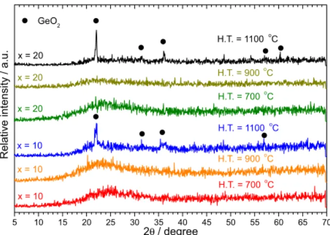
In Figure 3 are shown the XRD patterns for x = 10 and 20 doped with 1 mol% of Er3+ heat treated at 700,
900 and 1100 oC, where the peaks are indentified and
compared with those reported in the literature. A structural change clearly occurs as a function of the heat treatment temperature, which denotes a direct dependence of the crystalline phase contents. A large background between 15º and 35º in 2θ was detected in all diffractograms, which corresponds to the amorphous silica-based host, as also observed by Ferrari et al.27 for SiO
2-Ta2O5 compounds. In
accordance with JCPDS card number 73-1306, the peaks at 22.5; 31.5; 36.1; 48.7; and 57.1 degree are due to (101); (102); (112) and (200); (212); (213) and (301) planes of GeO2 nanocrystals with tetragonal structure (space group
P41212 (92)) and the cell parameters are a = 4.99 Å, and
c = 7.06 Å (C = 1.4148 and Z = 4). From the XRD results, the GeO2 crystals into the silicate host appear only after
heat treatment at 1100 oC.
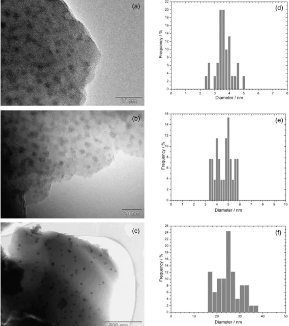
Morphological properties
Figures 4a and 4d show TEM images of the compounds annealed at 900 oC for 2 h containing x = 10, in which
spherical GeO2 nanoparticles of 3.7 ± 0.1 nm in diameter
is dispersed into the silicate host (which were not detected by XRD results). For the compounds with x = 20 annealed
5 10 15 20 25 30 35 40 45 50 55 60 65 70
H.T. = 900o
C
H.T. = 700o C
H.T. = 900o C x = 20
x = 20
x = 20
x = 10
x = 10
x = 10
H.T. = 1100o
C
H.T. = 1100oC
GeO2
R
e
la
ti
v
e
in
te
n
s
ity
/
a
.u
.
2θ/ degree
H.T. = 700o C
Figure 3. X-ray diffraction patterns for powders of (1 – x)SiO2:xGeO2 with x = 10 and 20 heat treated at 700, 900 and 1100 oC.
5 10 15 20 25 30 35 40 45 50 55 60 65 70
H.T. = 900o C
H.T. = 700o C
H.T. = 900o
C x = 20
x = 20
x = 20
x = 10
x = 10
x = 10
H.T. = 1100o
C
H.T. = 1100oC
GeO2
R
e
la
ti
v
e
in
te
n
s
ity
/
a
.u
.
2θ/ degree
H.T. = 700o
at 900 oC, Figures 4b and 4e, spherical GeO
2 nanoparticles
of around 4.6 ± 0.2 nm in diameter can be observed, and for x = 20 heat-treated at 1100 oC the diameter size increase to
25.0 ± 0.8 nm (Figures 4c and 4f). In fact, the diameter size of GeO2 nanocrystals is almost the same as the content of
the germanium oxide increases, at least for concentration of 10 and 20 mol%. Due to low crystallinity and the small size of the GeO2 nanoparticles, they were not detected by XRD
patterns (Figure 3) after annealing at 900 oC. Increasing the
annealing to 1100 oC for x = 20, GeO
2 nanoparticles with
higher diameter were crystallized and consequently could be detected by XRD patterns (Figure 3).
All the samples show GeO2 nanoparticles with diameter
lower than λ/20, considering as λ the wavelength of the
Er3+ pumping (λ = 980 nm, λ/20 = 49 nm) and emission
(λ = 1540 nm; λ/20 = 77 nm) used in telecommunication systems as optical amplifiers. Therefore, the presence of GeO2 nanoparticles will not reduce significantly the NIR
propagation signal, i.e., the contribution to the losses due to volume scattering is not significant considering these compositions in waveguides for infrared light.28,29 Besides,
films heat-treated around 700 oC could be even better for
waveguide application, since at these temperatures any GeO2 nanoparticles are distributed in the silicate host.
To evaluate the dispersion behavior of Er3+ ions in x = 20
compounds heat-treated at 900 oC and 1100 oC, were used
can see in Figure 5. For 900 oC, note that a higher erbium
peak intensity in GeO2 nanoparticles in comparison to that
in silicate matrix region. However, for 1100 oC in which
nanoparticles have diameter of around 25.0 ± 0.8 nm, a much higher concentration of Er3+ ions around/into the
GeO2 nanoparticles than in silica-rich matrix is observed,
indicating that Er3+ solubility in GeO
2 nanoparticles
are higher than in silicate host, especially at higher temperatures.
The chemical procedure developed here allows obtaining stable and uniform −Si−O−Ge−O−Si− network in sols, gels and films as well as powders synthesized at relative low temperatures. With heat-treatment phase separation was observed. It is well known that different ions segregate in silica network, as shown for SiO2-ZrO2,28,30
SiO2-TiO2,31 and SiO2-Ta2O527,29 leading to nanocrystals.
The same effect occurs for SiO2-GeO2 system studied here.
Increasing the energy (heat-treatment temperature) and the Ge content into the matrix, more ions quantity are expelled
from SiO2 network progressively and due to this the GeO2
particles into silica matrix increase in size significantly only at 1100 oC. On the other hand, the literature have mentioned
that rare-earth solubility in silica is < 1018 ions cm-3,32 and
we have shown in this work that larger amounts of Er3+
are located around/into GeO2 particles by EDX results,
confirming the Er3+ migration in samples heat treated at
high temperatures.
Optical properties
Gels
An illustrative image of the obtained gel is included in the Figure 6 took by a digital camera. Also, in Figure 6 we present a UV-Vis-NIR spectrum of the 90SiO2:10GeO2
gel doped with 1 mol% of Er3+. Similar results were
obtained for different concentrations of Er3+ and for x = 20
(not shown here). The gels were well transparent with high mechanical resistance allowing be handled. The f-f transitions of the Er3+ ions were detected at 269, 322, 366,
378, 406, 452, 489, 521, 547, 653, 886, 981 and 1490 nm from 4I
15/2 level to 4G9/2, 2P3/2, 2G9/2, 4G11/2, 2H9/2, 4F3/2, 4F7/2, 2H
11/2, 4S3/2, 4F9/2, 4I9/2, 4I11/2 and 4I13/2 level, respectively. The
bands centered at 1161, 1226, 1339, 1350, 1363, 1600, 1664, 1703, 1720, 1745, 1782, 1812, 1857, and 1937 nm are due to organic compounds (CH3, CH2, C−H, C−C, C=C,
C−O, C=O, C−N, C=N, O−H, N−H, N-O, and/or N=O, etc.) into the gel from precursor compounds.
Powders
Photoluminescence emission spectra in the near infrared region under excitation at 488 nm from the different powders changing composition and doping levels were obtained. In Figure 7a is illustrated the PL emission due to 4I
13/2→4I15/2
transition of Er3+ ions in the 90SiO
2:10GeO2 powders
heat-treated at 900 oC for different Er3+ concentrations, in the
0 1000 2000 3000 4000 5000 6000 7000
Er
Er Si
Ge
O
Nanoparticle (black spheres) Matrix In te n s it y / a .u .
Energy / eV x = 20 H.T. 900oC
0 1000 2000 3000 4000 5000 6000 7000
x = 20 H.T. 1100oC
In te n s it y / a .u .
Energy / eV
Nanoparticle (black spheres) Matrix Ge Er Si Er O (a) (b)
Figure 5. EDX spectra of x = 20 doped with 1 mol% of Er3+ heat-treated at 900 oC and 1100 oC. The thin lines are EDX spectra in a light gray region (matrix) and the thick lines are EDX spectra in a dark gray region (nanoparticles = black spheres) measured by TEM (Figures 4b and 4c,
respectively). 200 300 400 500 600 1000 1200 1400 1600 1800 2000
0 10 20 30 40 50 60 70 80 90 100 16 15 4 3 2 T ra n s m it ta n c e / %
Wavelength / nm 1 7 8 10 12 1314 17 18 19 20 21 22 23 24 25 26 27 5 6 9 11
Figure 6. Transmission spectrum in the UV-Vis-NIR regions for gels with x = 10 doped with 1 mol% of Er3+ and dried at 45 oC during 6 days.
0 1000 2000 3000 4000 5000 6000 7000
Er
Er Si
Ge
O
Nanoparticle (black spheres) Matrix In te n s it y / a .u .
Energy / eV
x = 20 H.T. 900oC
0 1000 2000 3000 4000 5000 6000 7000
x = 20 H.T. 1100oC
In te n s it y / a .u .
Energy / eV
Nanoparticle (black spheres) Matrix Ge Er Si Er O (a) (b)
200 300 400 500 600 1000 1200 1400 1600 1800 2000 0 10 20 30 40 50 60 70 80 90 100 16 15 4 3 2 T ra n s m it ta n c e / %
inset were included the integrated band intensity of these spectra as a function of Er3+ concentration. Note that the
PL emission increase from 0.05 to 0.5 mol% Er3+, and
higher concentrations the PL emission decrease gradually, showing that for x = 10 and annealing at 900 oC the best
rare-earth doping is around 0.5 mol%, being for this matrix the solubility limit. Increasing the heat treatment to 1100 oC
(Figure 7b), the PL emission maximum is observed for 0.8 mol% (almost the same intensity of 0.5 mol% sample) but the emission intensities are lower than that observed for 900 oC.
This is an indication that the Er3+ ions have higher
solubility around/into GeO2 in comparison with silicate host.
This is supported by EDX results (Figure 5) that show high concentrations of Er3+ ions around/into GeO
2 nanoparticles
at 1100 oC. However, increasing the temperature, it can
favor Er−O−Er clusters formation, which increases energy migration. Besides, the crystallization process, in which Ge−O−Ge, Si−O−Ge and Si−O−Si links breakdown, leads to the formation of defects and non-binding oxygens that favor Er3+ ions non-radiative de-excitation and reduce its
infrared emission. Probably the energy migration (due to Er−O−Er cluster formation) combined with presence of defects are the main contributions to the observed decrease in intensity for the samples containing higher than 0.8 or 0.5 mol% Er3+.
Note that, the annealing temperature is fundamental to activate Er3+ ions in the 90SiO
2:10GeO2 host, in fact
the 900 oC is the most appropriate temperature, when
compared to 1100 oC, being limited to 0.5 mol% of
Er3+ and presenting 30 nm of FWHM (full width at half
medium). This concentration limit value is higher than of Er3+ doped silica, aluminates and phosphates materials.33-35
The SiO2:GeO2 compositions have potential use as optical
amplifiers in integrated systems. In addition, their refractive index are slightly higher than that of silica allowing low losses in silica optical fibers coupling, and the presence of germanium enable diffraction gratings recording using UV lasers by photo-contraction phenomenon.9,10
At 1100 oC the FWHM of the emission centered at
1535 nm is around 13 nm, which are smaller than those observed for 900 oC, due to the presence of Er3+ ions around/
into GeO2 nanoparticles with higher size and crystallinity
(Figures 3 and 4).
Besides, when the GeO2 concentration is increased to
x = 20 (80SiO2:20GeO2) and doped with 1 mol% is observed
an emission 4.9 times superior than for x = 10, as presented in Figure 7c. Also, the NIR emission spectra were collected for both samples x = 10 and 20 containing 1 mol% of Er3+
and heat-treated at 1100 oC under excitation at 980 nm light
from a diode laser (spectra were not shown here), in which was observed the same emission intensity relation among both samples and same spectral shape in comparison to those spectra collected under 488 nm excitation. In previous EDX results, it was observed a higher erbium concentration around/into GeO2 nanoparticles, leading us to think that
GeO2 crystalline nanoparticles possess higher erbium
solubility in comparison to silicate host, preventing clustering 1480 1500 1520 1540 1560 1580 1600
0 100 200 300 400 500
0.0 0.2 0.4 0.6 0.8 1.0 1.2 1.4 1.6 1.8 2.0 0 2000 4000 6000 8000 10000 12000 14000
H.T. 900oC
x = 10
Intens
ity
/
a.u.
Wavelength / nm
2 mol% Er 1 mol% Er 0.8 mol% Er 0.5 mol% Er 0.3 mol% Er 0.1 mol% Er 0.05 mol% Er
B a n d a re a / a .u .
Er concentration / mol%
1480 1500 1520 1540 1560 1580 1600 0 10 20 30 40 50 60 70
0.0 0.2 0.4 0.6 0.8 1.0 1.2 1.4 1.6 1.8 2.0 0 200 400 600 800 1000 1200 1400 1600 1800 In te n s it y / a .u .
Wavelength / nm
2 mol% Er 1 mol% Er 0.8 mol% Er 0.5 mol% Er 0.3 mol% Er 0.1 mol% Er 0.05 mol% Er
H.T. 1100o C
x = 10
B a n d a re a / a .u .
Er concentration / mol%
1480 1500 1520 1540 1560 1580 1600 0 50 100 150 200 250
H.T. 1100o C
1 mol% Er
x = 20 x = 10
In te n s it y / a .u .
Wavelength / nm
10 20 0 1000 2000 3000 4000 5000 6000 B a n d a re a / a .u . x value 4.9x (a) (b) (c)
Figure 7. PL emission spectra under 488 nm excitation for powders doped with different erbium concentrations of: (a) x = 10 composition, and heat-treated at 900 oC; (b) x = 10 composition, and heat-treated at 1100 oC; (c) x = 10 and 20, doped with 1 mol% of Er3+, and heat-treated at 1100 oC.
1480 1500 1520 1540 1560 1580 1600
0 100 200 300 400 500
0.0 0.2 0.4 0.6 0.8 1.0 1.2 1.4 1.6 1.8 2.0 0 2000 4000 6000 8000 10000 12000 14000
H.T. 900oC
x = 10
Intens
ity
/
a.u.
Wavelength / nm
2 mol% Er 1 mol% Er 0.8 mol% Er 0.5 mol% Er 0.3 mol% Er 0.1 mol% Er 0.05 mol% Er
B a n d a re a / a .u .
Er concentration / mol%
1480 1500 1520 1540 1560 1580 1600
0 10 20 30 40 50 60 70
0.0 0.2 0.4 0.6 0.8 1.0 1.2 1.4 1.6 1.8 2.0 0 200 400 600 800 1000 1200 1400 1600 1800 In te n s it y / a .u .
Wavelength / nm
2 mol% Er 1 mol% Er 0.8 mol% Er 0.5 mol% Er 0.3 mol% Er 0.1 mol% Er 0.05 mol% Er
H.T. 1100o
C
x = 10
B a n d a re a / a .u .
Er concentration / mol%
1480 1500 1520 1540 1560 1580 1600
0 50 100 150 200 250
H.T. 1100o
C
1 mol% Er
x = 20 x = 10
In te n s it y / a .u .
Wavelength / nm
and formation of Er−O−Er links (at least for the samples containing Er3+ concentration lower than 0.5 mol%).
Since the luminescence intensity for the both samples (x = 10 and x = 20) annealed at 900 oC doped with 1 mol%
of Er3+ are similar in NIR region, it was presented in Figure 7
only emission spectra concerning the x = 10 samples. However, when the samples are annealed at 1100 oC the
x = 20 sample have higher emission intensity in comparison with that containing x = 10. This can be explained by the hydroxyl groups reduction and relevant portion of Er3+
ions migration to nanocrystals (as shown by EDX results). Moreover, GeO2 compounds have lower phonon energy
(740 cm-1)36 than SiO
2 compounds (1075 cm-1)27 favoring an
improvement of the Er3+ NIR emission. The EDX technique
has no high precision to determine the exact Er3+ position,
i.e., it is not known exactly if they are in higher quantity into or around GeO2 particles. Also, in samples with x = 20
heat-treated at high temperatures (1100 oC) occurs the formation of
higher crystalline GeO2 particles size than for x = 10, which
gives a different light scattering (in excitation and emission), but a higher Er3+ solubility associated to low phonon energy
can compensate some intensity decrease due to scattering. Likewise, to study the heat treatment effect and GeO2
content, the PL decay curves were measured at 1535 nm from 4I
3/2 level of Er3+, the medium lifetime values were
listed in Table 1. In x = 10 with 1 mol% of Er3+ occurs
the lifetime changes from 15.0 ± 0.5 ms for 900 oC
to 7.5 ± 0.5 ms 1100 oC, but when GeO
2 is increased
(x = 20) the lifetime is about 12.8 ± 0.5 ms for 1100 oC,
corroborating with our previous results and discussions, i.e., low GeO2 concentration associate to high temperature
promote some Er−O−Er clustering or defects generation that reduce active Er3+ ions, and high temperatures with
higher GeO2 concentration increase active Er3+ ions. In
fact, the Er3+ infrared PL emissions, lifetime values and
structural properties of the host are strongly correlated.
The lifetime value for 4I
13/2 level of Er3+ ions in the x = 20
composition heat-treated at 1100 oC is comparable to those
values measured by Sigoli et al.21 for 95.8SiO2:4.2GeO2
host, which changed between 13.2 and 11.3 ms depending on the Er3+ and Yb3+ contents.
Thin films
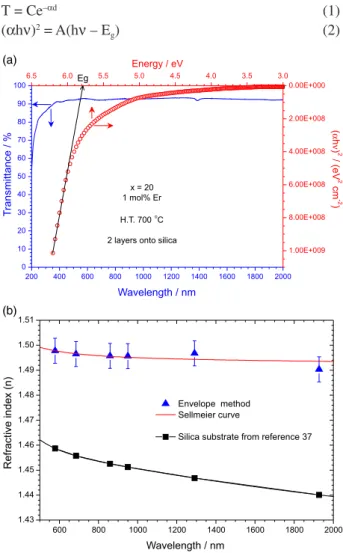
Optical transmission spectra of the 80SiO2:20GeO2 films
doped with 1 mol% of Er3+ were measured continuously from
200 nm to 2000 nm with an UV-Vis-NIR spectrophotometer. Figure 8a displays the transmission spectra of film with 3 layers heat-treated at 700 oC. A high transparency in
the visible and infrared regions was detected, higher than 92% at 632.8 nm (the He-Ne laser wavelength used as reference). Other optical property, such as the band gap, was obtained indirectly. Considering the high absorption region, the transmittance (T)followed a simple correlation with absorption coefficient,37 equation 1, where C is
approximately equal to the unity at the absorption edge and dis the thickness of the thin films. The relation between the absorption coefficient αand incident photon energy hν for allowed direct transition can be written as equation 2,37 where
Ais constant and Eg is the direct band gap.
T = Ce–αd (1)
(αhν)2 = A(hν – E
g) (2)
Table 1. Lifetime value for 4I
13/2 level of Er3+ ions in the compositions with x = 10 and 20, and heat-treated at 900 or 1100 oC
Sample Er3+ doping / mol%
Heat treatment / oC
Er3+4I 13/2 lifetime / ms
x = 10 1.0 900 15.0 ± 0.5
x = 10 1.0 1100 7.5 ± 0.5
x = 20 1.0 1100 12.8 ± 0.5
200 400 600 800 1000 1200 1400 1600 1800 2000
0 10 20 30 40 50 60 70 80 90 100
Wavelength / nm
T
ransmittance / %
x = 20 1 mol% Er
H.T. 700o C
2 layers onto silica
6.5 6.0 5.5 5.0 4.5 4.0 3.5 3.0
1.00E+009 8.00E+008 6.00E+008 4.00E+008 2.00E+008 0.00E+000
Energy / eV
(
α
h
ν
) 2
/(
eV
2
cm
-2
)
Eg
600 800 1000 1200 1400 1600 1800 2000
1.43 1.44 1.45 1.46 1.47 1.48 1.49 1.50 1.51
Envelope method Sellmeier curve
Silica substrate from reference 37
Refr
a
ct
ive
in
d
e
x
(n
)
Wavelength / nm
(a)
(b)
Figure 8. (a) Transmission spectra in the UV-Vis-NIR region for film with x = 20 doped with 1 mol% of Er3+, deposited by spin-coating onto silica substrate (3 layers), and heat-treated at 700 oC; (b) refractive index values dispersion and Sellmeier curve for x = 20 and values for silica substrate.
200 400 600 800 1000 1200 1400 1600 1800 2000
0 10 20 30 40 50 60 70 80 90 100
Wavelength / nm
T
ransmittance / %
x = 20 1 mol% Er
H.T. 700o
C
2 layers onto silica
6.5 6.0 5.5 5.0 4.5 4.0 3.5 3.0
1.00E+009 8.00E+008 6.00E+008 4.00E+008 2.00E+008 0.00E+000 Energy / eV
(
α
h
ν
) 2
/(
eV
2
cm
-2
)
Eg
600 800 1000 1200 1400 1600 1800 2000
1.43 1.44 1.45 1.46 1.47 1.48 1.49 1.50 1.51
Envelope method Sellmeier curve
Silica substrate from reference 37
Refr
a
ct
ive
in
d
e
x
(n
)
Wavelength / nm (a)
The (ahν)2versus hν plot for the thin film is shown in
Figure 8a. A linear behavior can be observed in a certain range of the curves, supporting the interpretation of direct Egband gap for thin film.37 Therefore, the Egband gap can
be obtained by extrapolating relation (2) around 5.79 eV (214 nm). This value is comparable with those reported by Jing et al.16 of 5.5 eV (225 nm) for 30SiO2:70GeO2
thick films. On the other hand, works on glasses with 90SiO2:10GeO2 composition developed by Nishii et al.38
and Shigemura et al.17 obtained an optical band gap of
ca. 7.1 eV (175 nm), and ca. 6.0 eV (207 nm), respectively. All these values is influenced by the GeO2 nanosized into
the matrix and an absorption band at ca. 5 eV (248 nm) assigned to different kinds of intrinsic germanium-related oxygen-deficient centers in glasses, which consist of neutral oxygen monovacancy [(NOMV)≡Ge−Ge≡ or ≡Ge−Si≡] and neutral oxygen divacancy [(NODV)-Ge2+].16,17,39 In
our optical transmission spectra (Figure 8a) was not observed the band associated to these defects, indicating that we have films with high optical quality without structural defects.
The refractive index (n) and film thickness could be determined from the interference fringes by the envelope method, using the expression reported by Manifacier et al.40
and modified by Peng and Desu,41 equation 3, where N is
defined with equation 4. Tmax and Tmin are the transmission
maximum and the corresponding minimum at a wavelength
λ of the interference fringes (Figure 8a), while ns is the
substrate refractive index silica at the same wavelength.42
The refractive index values, n, calculated from equations 3 and 4, are shown in Figure 8b for 80SiO2:20GeO2 films
annealed at 700 oC. The refractive index results have been
fitted with the following Sellmeier curve,43 equation 5.
( )
[ 2 21/2]1/2
s n N N
n = + − (3)
( ) ( )
( max min)
min max 2
. 2
1 5 . 0
T T
T T n n
N= + s + s − (4)
2
3 2
3 2
10 10
− −
+
= λ
λ C D
B A
n (5)
The fit of the experimental results with equation 5 provides the following set of parameters: A = 2.2315; B = 0.0040; C = 0.0030; and D = 0.0005 (λ in nm). This Sellmeier curve is shown in Figure 8b. The calculated refractive index presents a good dispersion and it can be well fitted by the Sellmeier relation. The extrapolated values of the Sellmeier curves can be used to calculate the
admittance angle and coupling angle when 80SiO2:20GeO2
amorphous is used in waveguiding experiments.
Another application of transmission spectra is the film thickness estimation. The thickness d of the layer can be calculated from two adjacent maxima or minima of interference fringes at λ1 and λ2 by equation 6,41 where λ1,
n(λ1) and λ2, n(λ2) are the corresponding wavelengths and
refractive indexes calculated above by the envelope method. The average value of d determined by the equation 6 is 1214 ± 35 nm.
(
)
( )
( )
[
1 2 2 1]
2 1
. .
2
.
λ λ λ λ
λ λ
n n
d
−
= (6)
The refractive index of the bulk glass material is 1.489 at 589.3 nm wavelength.44 In this work we obtained a refractive
index of 1.498, which is similar than that of 80SiO2:20GeO2
glass, indicating a high density of our films annealed at 700 oC. This film heat-treated at 700 oC is very important
for waveguide design; in the present case, one has a high
∆n = 0.040 at 589.3 nm, ∆n= 0.040 at 632.9 nm, ∆n= 0.050 at 1535 nm wavelengths between the waveguiding layer and the SiO2 buffer layer (or cladding), such that a guiding layer
thickness of 787 nm is already sufficient for single mode propagation (TE0 or TM0 mode) at 1535 nm. To excite the
second mode (TE1 or TM1), it is necessary to have a film with 2790 nm thickness (these thickness limit values were calculated by relation in the reference 25).
Sigoli et al.21 have obtained a refractive index of
ca. 1.453 at 1550 nm for the film thermally treated at 1150 oC with an average thickness of ca. 3.9 mm. The
refractive index was lower than that obtained in our work (ca. 1.49) because we used larger amounts of GeO2 that
allow prepare thinner films to have only one guided mode, i.e., thickness of ca. 1.2 mm is enough to guide the first mode (TE0 or TM0 mode) in the films of 80SiO2:20GeO2
matrix. Probably, films of x = 20 composition having thickness around ca. 2500 nm (6 layers) should be adequate to be applied as waveguides in the NIR region.
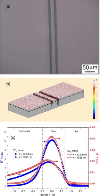
An 800 nm Ti-sapphire laser emitting 150 fs, 76 MHz mode-locked pulses was focused on the film surface by an objective lens. The spot size of the focused beam was 5 mm at the focal point, and the average power of the laser was 10 mW. The scanning speed was 0.5 mm s-1. Optical
grooves there is the waveguide consisting of the Er-doped 80SiO2:20GeO2 ribs on silica substrate. The air grooves
with a width around 10 mm and a depth of 5 mm, were created by the laser irradiation and the shape and structure of channels are highly reproducible and sharply defined (Figures 9a and 9b). The width and depth of the channels can be tailored changing the position of the spot of the focused beam in order to produce mono or multimodal channel waveguides. In our preliminary experiment we obtained ribs with width of 15 mm.
On the basis of the film thickness and refractive index values, the confinement coefficient of the film
was estimated. Figure 9c shows the squared electric and magnetic field profiles of the TE0 and TM0 modes of the
waveguides containing with x = 20 at 632.8 and 1535 nm wavelengths. The values represent the ratio of the integrated intensity, i.e., the square of the electric or magnetic field in the waveguide to the total intensity for each wavelength. The total intensity also includes the squared evanescent fields.30 A light confinement above 82% can be seen for
the waveguides excited at 632.8 nm. For the 1535 nm wavelength, the TE0 and TM0 confinement are ca. 50%
and ca. 46%. Higher confinement coefficients for TE0 and
TM0 modes are expected by increasing the film thickness
and it is possible to obtain a well confined single mode at 1535 nm, which is the wavelength of interest in integrated optical systems as amplifiers.
The differences between the refractive index of the rib channel waveguide and silica optical fibers are crucial to its application as waveguide amplifiers in telecommunication systems, as well as the rib channel waveguide thickness. The losses by coupling with silica optical fibers increases in compounds with high refractive index and low thickness. In fact, it is necessary to tailor the refractive index and thickness of the rib channel in relation to the commercial optical fibers. But, the refractive index of the rib channel cannot be low, because they are deposited onto silica (same material of the optical fibers), if not the pump and emitted light did not maintain confined. On the other hand, the losses in this sol-gel based planar waveguides are not only due to these parameters. During sol synthesis and film deposition undesirable impurities can be incorporated and/or not be eliminated by heat-treatments, resulting in waveguides with losses of about 1.0 dB cm-1.28 Although
full densification is always achieved together with initial crystallization process, crystalline size need be controlled.25
Surface roughness should be considered as another source of losses, to reduce these losses the homogeneous and crack-free films should be prepared. Finally, the best composition reported in our work (80SiO2:20GeO2) is
close in composition to other systems in the literature, for example, those containing ZrO2,28,30 TiO2,31 and T2O5,27,29
however present lower refractive index.
Conclusions
In summary, we have used a simple sol-gel route to prepare stable and transparent sols, gels and films. The gels decompositions to form powders were evaluated by TGA and DTA techniques, and endothermal and exothermal events were analyzed. The materials show mass loss from room temperature to around 500 oC.
Between 500 and 700 oC, no reactions were observed. The Figure 9. (a) Optical surface image; (b) 3D image of the 15 mm width
organic and hydroxyl compounds into the matrix were evaluated by FTIR that reduce gradually by increasing the annealing temperature. At 700 oC, the materials are
completely amorphous, but at higher temperatures a silica-rich amorphous phase and GeO2 nanocrystals with
tetragonal structure were obtained. The HRTEM images reveal spherical GeO2 nanoparticles of around 3.7, 4.6
and 25.0 nm in diameter for x = 10 at 900 oC, x = 10 and
x = 20 at 1100 oC, respectively. EDX results show high
concentrations of Er3+ ions around GeO
2 nanoparticles at
1100 oC. In fact, the GeO
2 nanoparticles formation can
allow incorporate higher concentration of active Er3+ ions.
For x = 10, higher infrared emissions occur in the matrix doped with 0.5 mol% of Er3+, at 900 oC and 1100 oC. But
the 1 mol% of Er3+ doped 80SiO
2:20GeO2 compound have
an infrared emission around 4.9 times higher than that for 1 mol% Er3+ doped 90SiO
2:10GeO2. The Er3+4I13/2 level
has a lifetime between 15.0 ms and 7.5 ms depending on the GeO2 content and heat-treatment. The optical
band gap of 5.79 eV and refractive index values were determined, being ca. 1.498 at wavelength of 589.3 nm, and the Sellmeier parameters were estimated. Films deposited by spin-coating technique present ca. 1214 nm thickness, as calculated by the envelope method. Rib channel waveguides were obtained with width of 15 mm using femtosecond laser radiation, and a light confinement above 82% can be achieved for these waveguides when excited at 632.8 nm.
The chemical procedure using as a precursor TEOS, GeO2, TMAH is easy, doesn’t require special atmosphere,
and has relatively low cost. As a final conclusion, the 1mol% of Er3+ doped 80SiO
2:20GeO2 compounds are
potentially applicable in integrated optical systems, specially as miniaturized optical amplifiers.
Supplementary Information
Supplementary data (PL spectra) are available free of charge at http://jbcs.sbq.org.br as PDF file.
Acknowledgements
The authors are grateful for the financial support provided by CAPES, CNPq, FAPEG, FAPESP and FUNAPE/UFG Brazilian agencies.
References
1. Henmi, N.; Aoki, Y.; Ogata, T.; Saito, T.; Nakaya, S.;
J. Lightwave Technol.1993, 11,1615.
2. Krokhin, O. N.; Laser Phys.2005, 15,1303.
3. Mukhopadhyay, S.; Ramesh, K. P.; Kannan, R.; Ramakrishna, J.;
Phys. Rev. B2004, 70,224202.
4. Polynkin, O.; Temyanko, V.; Mansuripur, M.; Peyghambarian, N.;
IEEE Photon. Technol. Lett. 2004, 16,2024.
5. Cheng, C.; Xiao, M.; Opt. Commun. 2005, 254, 215. 6. Dejneka, M. J.; Hanson, B. Z.; Crigler, S. G.; Zenteno, L. A.;
Minelly, J. D.; Allan, D. C.; Miller, W. J.; Kuksenkov, D.; J. Am. Ceram. Soc. 2002, 85, 1100.
7. Bulla, D. A. P.; Li, W. T.; Charles, C.; Boswell, R.; Ankiewicz, A.; Love, J. D.; J. Lightwave Technol. 2005, 23, 1302.
8. Armelao, L.; Gross, S.; Obetti, G.; Tondello, E.; Surf. Coat. Technol. 2005, 190, 218.
9. Nunzi-Conti, G.; Berneschi, S.; Brenci, M.; Pelli, S.; Sebastiani, S.; Righini, G. C.; Tosello, C.; Chiasera, A.; Ferrari, M.; Appl. Phys. Lett.2006, 89, 121102.
10. Pita, R. K.; Yu, S. F.; Tjin, S. C.; Kam, C. H.; Appl. Phys. Lett.
2006, 89, 071105.
11. Qin, G.; Lu, J.; Bisson, J. F.; Feng, Y.; Ueda, K. I.; Yagi, H.; Yanagitani, T.; Solid State Commun. 2004, 132, 103. 12. Schubert, U.; Arpac, E.; Glaubitt, W.; Helmerich, A.; Chau, C.;
Chem. Mater. 1992, 4, 291.
13. Liu, J.; Lam, Y. L.; Chan, Y. C.; Zhou, Y.; Que, W. X.; Ooi, B. S.; Appl. Phys. A1999, 69, 649.
14. Chang, C. C.; Chen, W. C.; Chem. Mater. 2002, 14, 4242.
15. Zourob, M.; Mohr, S.; Fielden, P. R.; Goddard, N. J.; Lab Chip
2005, 5, 772.
16. Jing, C.; Hou, J.; Zhang, Y.; J. Phys. D: Appl. Phys. 2006, 39, 1174.
17. Shigemura, H.; Kawamoto, Y.; Nishii, J.; Takahashi, M.; J. Appl. Phys. 1999, 85, 3413.
18. Jang, J. H.; Koo, J.; Bae, B. S.; J. Non-Cryst. Solids1999, 259, 144.
19. Yang, H.; Yao, X.; Wang, X.; Gu, X.; Wang, F.; Opt. Mater. 2007, 29, 631.
20. Que, W.; Wang, L. L.; Chen, T.; Sun, Z.; Hu, X.; J. Cryst. Growth
2006, 288, 75.
21. Sigoli, F. A.; Messaddeq, Y.; Ribeiro, S. J. L.; J. Sol-Gel Sci. Technol.2008, 45, 179.
22. Jing, C.; Hou, J.; Zhang, Y.; J. Am. Ceram. Soc. 2007, 90, 3646.
23. Siemens A. G.; Coating Germanium Crystals with a Water Insol Germanium Oxide, US pat. 3,525,650-A1965 (CA 842735-A).
24. Miller, S. E.; IEEE J. Quantum Electron. 1972, QE-8 part 2, 199.
25. Lee, D. L.; Electromagnetism Principles of Integrated Optics; Wiley: New York, USA, 1986.
26. de Pietro, G. M.; Pereira, C.; Gonçalves, R. R.; Ribeiro, S. J. L.; Freschi, C. D.; Cassanjes, F. C.; Poirier, G.; J. Am. Ceram. Soc., in press, DOI: 10.1111/jace.13555.
28. Gonçalves, R. R.; Guimarães, J. J.; Ferrari, J. L.; Maia, L. J. Q.; Ribeiro, S. J. L.; J. Non-Cryst. Solids2008, 354, 4846.
29. Ferrari, J. L.; Lima, K. O.; Maia, L. J. Q.; Ribeiro, S. J. L.; Gomes, A. S. L.; Gonçalves, R. R.; J. Nanosci. Nanotechnol.
2011, 11, 2540.
30. Cunha, C. S.; Ferrari, J. L.; Oliveira, D. C.; Maia, L. J. Q.; Gomes, A. S. L.; Ribeiro, S. J. L.; Gonçalves, R. R.; Mater. Chem. Phys.2012, 136, 120.
31. Almeida, R. M.; Marques, A. C.; Pelli, S.; Righini, G. C.; Chiasera, A.; Mattarelli, M.; Montagna, M.; Tosello, C.; Gonçalves, R. R.; Portales, H.; Chaussedent, S.; Ferrari, M.; Zampedri, L.; Philos. Mag.2004, 84, 1659.
32. Maia, L. J. Q.; Mastelaro, V. R.; Hernandes, A. C.; Fick, J.; Ibanez, A.; Thin Solid Films2009, 517, 6584.
33. Melkumov, M. A.; Laptev, A. Y.; Yashkov, M. V.; Vechkanov, N. N.; Guryanov, A. N.; Bufetov, I. A.; Inorg. Mater.2010, 46,
299.
34. van den Hoven, G. N.; Polman, A.; Van Dam, C.; Van Uffelen, J. W. M.; Smit, M. K.; Appl. Phys. Lett. 1996, 68, 1886. 35. Kik, P. G.; Polman, A.; MRS Bull. 1998, 23, 48.
36. Jha, A.; Richards, B.; Jose, G.; Teddy-Fernandez, T.; Joshi, P.; Jiang, X.; Lousteau, J.; Prog. Mater. Sci.2012, 57, 1426.
37. Maia, L. J. Q.; Bernardi, M. I. B.; Feitosa, C. A. C.; Mastelaro, V. R.; Zanatta, A. R.; Hernandes, A. C.; Thin Solid Films2004,
457, 246.
38. Nishii, J.; Kitamura, N.; Yamanaka, H.; Hosono, H.; Kawazoe, H.; Opt. Lett. 1995, 20, 1184.
39. Jang, J. H.; Koo, J.; Bae, B. S.; J. Am. Ceram. Soc. 2000, 83,
1356.
40. Manifacier, J. C.; Gasiot, J.; Fillard, J. P.; J. Phys. E: Sci. Instrum. 1976, 9, 1002.
41. Peng, C. H.; Desu, S. B.; J. Am. Ceram. Soc. 1994, 77, 929.
42. Mazurin, O. V.; Streltsina, M. V.; Shvaiko-Shvaikovskaya, T. P.; Handbook of Glass Data: Part A-Silica Glass and Binary Silicate Glasses; Elsevier: New York, USA, 1983.
43. Vázquez, R. M.; Osellame, R.; Marangoni, M.; Ramponi, R.; Diéguez, E.; Opt. Mater. 2004, 26, 231.
44. Doweidar, H.; J. Non-Cryst. Solids2011, 357, 1665.
Submitted: June 15, 2015 Published online: September 1, 2015