Strained In
1-xGa
xAs
yP
1-y/InP Quantum Well Heterostructures
Grown by Low-Pressure Metalorganic Vapor Phase Epitaxy
Wilson de Carvalho Jr
a*, Ayrton André Bernussi
a, Mário Tosi Furtado
a,
Ângelo Luiz Gobbi
a, Mônica A. Cotta
baAssociação Brasileira de Luz Síncrotron,
Fundação Centro de Pesquisa e Desenvolvimento em Telecomunicações, Laboratório de Optoeletrônica, 13088-061 Campinas - SP, Brazil bUniversidade Estadual de Campinas, Instituto de Física Gleb Wattagin
Laboratório de Pesquisa em Dispositivos, 13083-970 Campinas - SP, Brazil *e-mail: [email protected]
Received: February 27, 1998; Revised: December 7, 1998
We have investigated the optical and the structural properties of strained In1-xGaxAsyP1-y/InP and strain compensated In1-xGaxAsyP1-y/In1-zGazAsqP1-q/InP multi-quantum well heterostructures grown by low-pressure metalorganic vapor phase epitaxy at different growth conditions. Our results indicate an increase of the compositional fluctuation of quaternary materials as the alloy composition moves from the outer spinodal isotherm into the miscibility gap region. In1-xGaxAsyP1-y layers grown at high tensile strained values exhibit a three-dimensional-like growth mode. Strain compen-sated structures revealed the presence of a broad photoluminescence emission band below the fundamental quantum well transition, well defined elongated features along the [011] direction and interface undulations. All these effects were found to be strongly dependent on the growth temperature and the number of wells.
Keywords: InGaAsP, InP, MOCVD, strain, multiple quantum wells, epitaxial growth
1. Introduction
In recent years In1-xGaxAsyP1-y/InP quaternary alloys
emitting in the near infrared spectral region have proved to be of fundamental technological importance, particularly due to their role as active layers in semiconductor laser diodes, photodetectors, optical amplifiers and modulators for teleco mmunication applications. The development of advanced epitaxial techniques such as Molecular-Beam Epitaxy (MBE), Chemical-Beam Epitaxy (CBE) and Meta-lorganic Vapor Phase Epitaxy (MOVPE), enabled the fab-rication of superior performance InGaAs(P)/InP strained quantum well heterostructures devices1-3. These new struc-tures also provide a great degree of freedom in the selection of chemical composition of In1-xGaxAsyP1-y alloys with a
considerably wide range of the optical spectral emission wavelengths varying from 1000 nm up to 2000 nm.
In this work, we investigated the optical and the struc-tural properties of strained In1-xGaxAsyP1-y /InP
heteros-tructures grown by low-pressure (LP) MOVPE at different
growth temperatures and with mismatches (ε) ranging from -0.75% to +1%, as well as strain compensated In1-xGa
x-AsyP1-y/In1-zGazAsqP1-q/InP multi-quantum well (MQW)
2. Experiment
The In1-xGaxAsyP1-y epitaxial layers were grown on
InP:S (100)-oriented substrates by LP-MOVPE at 70 Torr and growth temperature (TG) in the range of 640-670 °C.
Trimethylindium (TMIn) and triethylgallium (TEGa) or-ganometallic compounds were used as In and Ga sources, respectively, and phosphine (PH3) and arsine (AsH3)
hy-drides as P and As sources, respectively. The V/III ratios used were 280 for compressive layers and 380 for tensile layers.
We investigated three different types of heterostruc-tures: i) Type-I: strained In1-xGaxAsyP1-y (λ ~ 1670 nm, ε = +1% and λ ~ 1300 nm, ε = -0.5%) 30 nm thick followed by a InP cap layer 3 nm thick; ii) Type-II: tensile and compressive In1-xGaxAsyP1-y/InP-MQW structures, and iii)
Type-III: In1-xGaxAsyP1-y/In1-zGazAswP1-w/InP-MQW with
strain compensation. Type-I structures were used to calibrate the composition and the growth rate of single quaternary layers. The layer thickness of 30 nm was chosen in order to avoid strain relaxation and consequently the generation of dislocation defects. This thickness value is below the critical thickness for all layers analyzed in this work. The MQW type-II structures were used to evaluate the structural (inter-faces) and the optical quality of thin (8 and 4 nm) quaternary layers. Finally, the type-III structures consisted of strain com-pensated In1-xGaxAsyP1-y/In1-zGazAswP1-w/InP multilayers.
All the samples were analyzed by conventional optical microscopy, 300 K and 77 K photoluminescence, 300 K photoluminescence microscopy imaging, double crystal X-ray diffraction in both (400) and (200) reflections, and atomic force microscopy (AFM). The In1-xGaxAsyP1-y alloy
compositions were determined by combining the results of X-ray and PL measurements.
3. Results and Discussion
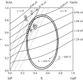
The In1-xGaxAsyP1-y alloy can be considered as a solid
solution, composed by four binaries: InP, InAs, GaAs and GaP. However, the large difference between the binary bond lengths gives rise to a solid miscibility gap region represented by a range of compositions and temperatures where the solid is thermodynamically unstable with a ten-dency to decompose into GaP- and InAs-rich phases7,8. Epitaxial layers grown close or inside the miscibility gap region may exhibit optical and structural proprieties infe-rior to those grown in the outer isotherm region. As a result, the device performance based on these materials may be strongly affected if the InGaAsP epitaxial layers were grown inside or in the vicinity of the miscibility gap region. Figure 1 shows the calculated composition diagram of InGaAsP alloys taking into account the strain effects on the band gap energy9. The solid and dashed straight lines represent constant strain compositions lattice matched and mismatched to InP, respectively. The small circles shown
in Fig. 1 represent the material compositions of In-GaAsP/InP samples analyzed in this work. The details of the sample structures are shown in Table 1. The calculated isoenergy line discontinuities, when these curves cross the lattice one, were attributed to the change in the optical transition energy from heavy- to light-hole with strain. The large elliptical regions represent the thermally unstable gap for TG = 640 °C (outer ellipse) and TG = 670 °C (inner
ellipse). The region inside the ellipse denotes the miscibil-ity gap for the quaternary system. The lower the growth temperature the higher is the miscibility gap region. As can be observed from Fig. 1 the tensile (ε < 0) strained layers analyzed in the present work were obtained inside or in the vicinity of the miscibility gap. However, the compressively (ε > 0) strained layers were grown outside the spinodal decomposition isotherm region.
Figure 2 shows the X-ray rocking curve for (200) re-flection and the photoluminescence spectra at T = 77 K of two different samples: i) compressive and ii) tensile layers with nominal strain values (ε) of +1% and -0.5%, respec-tively. The magnitude of the strain in each sample was directly evaluated from the X-ray spectra (Fig. 2a) by measuring the separation between the InP substrate peak and the layer ones. The obtained strain values were ε = -0.6% and ε = +1.1% for tensile and compressive layers, respectively. The PL spectra of compressive and tensile strained layers (Fig. 2b) exhibited a single emission band centered around E = 0.765 eV (λ = 1621 nm) and E = 0.986 eV (λ = 1258 nm), with PL linewidths (FWHM) of 18 meV
and 27 meV, respectively. The solid composition, deter-mined from the combination of PL and X-ray data, yields: i) x = 0.247, y = 0.870, for ε = +1.1% and ii) x = 0.419, y = 0.717 for ε = -0.6%.
The observed difference in the PL linewidth values (see Fig. 2b) of both samples suggests that the material grown under tensile strain has a larger density of defects and/or a larger compositional fluctuation when compared to the
Figure 2. X-ray diffraction pattern (a) and 77 K photoluminescence spectra (b) of compressive and tensile strained samples.
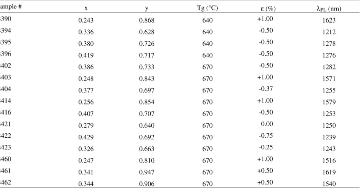
Table 1. Solid composition, nominal strain and PL wavelength peaks (at T = 77 K) for all samples shown in Fig. 1.
Sample # x y Tg (°C) ε (%) λPL (nm)
B390 0.243 0.868 640 +1.00 1623
B394 0.336 0.628 640 -0.50 1212
B395 0.380 0.726 640 -0.50 1278
B396 0.419 0.717 640 -0.50 1276
B402 0.386 0.733 670 -0.50 1282
B403 0.248 0.843 670 +1.00 1571
B404 0.377 0.697 670 -0.37 1255
B414 0.256 0.854 670 +1.00 1579
B416 0.407 0.707 670 -0.50 1253
B421 0.279 0.640 670 0.00 1250
B422 0.429 0.692 670 -0.75 1239
B423 0.326 0.663 670 -0.25 1243
B460 0.247 0.810 670 +1.00 1516
B461 0.341 0.947 670 +0.50 1619
material grown under compressive strain. In order to further understand this behavior, we show in Fig. 3 the PL spectra (normalized to unity) of the same tensile sample analyzed in Fig. 2 under four orders of magnitude of excitation power levels (Iexc). As can be seen from Fig. 3 the PL spectra are
strongly dependent on the excitation power level. At the lowest excitation power level the PL emission line is rela-tively broad (FWHM ~ 46 meV) and at least two peaks can be distinguished. At this excitation condition the intensity of the low energy emission band is slightly larger than the high energy one. As the excitation power increases the spectra become narrower and the high-energy peak domi-nates the spectra whereas the low-energy emission band practically disappears. A minimum value of FWHM = 25.3 meV was obtained at Iexc = 0.01Io (Io ~ 100 W/cm2). Above
this excitation power level the PL spectra starts to broaden again and reaches a maximum value of FWHM = 56.5 meV at Iexc = 0.32 Io. The double peaks observed in Fig. 3 at low
excitation power levels suggests the existence of an incom-plete segregation of InGaAsP into InAs-rich regions as a result of the alloy spinodal decomposition (see Fig. 1)10. As a consequence, the PL linewidth broadens due to the vari-ation of the InGaAsP alloy composition. As the excitvari-ation power level increases the recombination at the lower energy gap region (InAs-rich) saturates and favors the recombina-tion at the nominal alloy region. The competirecombina-tion between the two emission peaks explains the blue shift observed in Fig. 3 at increasing power densities. At high excitation power levels (Iexc > 0.01 Io) the high-energy side of the PL
spectrum broadens due the increase of lattice temperature at high pumping densities. The same type of analysis was used to investigate the effect of the excitation intensity on the PL spectra of the compressively strained sample. In this
case, only a single emission band was observed and the PL linewidth is essentially independent of the pumping power density in the excitation level range of 3.2 x 10⁻⁵ Io < Iexc < 1 x 10⁻² Io. The weak dependence of the PL
spectra on the excitation power and the significantly nar-rower linewidth of the compressive strained material sug-gest a reduced alloy fluctuation in this material. This behavior was attributed to the growth conditions of the compressive strained layers that were grown with compo-sition and temperatures outside the corresponding miscibil-ity gap region (see Fig. 1).
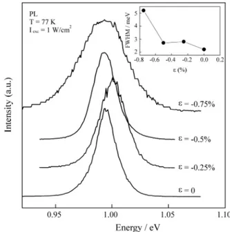
Another strong evidence of the spinodal decomposition effect on the properties of tensile strained layers can be obtained from the PL spectra (normalized to unity) of samples with different strain values as shown in Fig. 4. The PL linewidth increases from 23 meV to 53 meV (see insert of Fig. 4 ) when the magnitude of the tensile strain values was varied from ε = 0 to ε = -0.75%, respectively. The large increase of the PL linewidth at high tensile strain values was attributed to a larger composition fluctuation of the alloy layer that occurs inside the miscibility gap region (see Fig. 1).
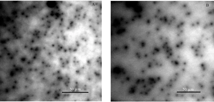
Room temperature integrated photoluminescence im-age microscopy was also used to investigate the properties of strained layer materials. Figures 5a and 5b show the PL image of a tensile (ε = -0.5%) and a compressive (ε = +1%,) strained layer, respectively. The PL images exhibit a high density of dark spots (4.7 x 105 cm-2 for the tensile layer and 3.4 x 105 cm-2 for the compressive strained layer) with an average diameter of 1 µm. These dark spots were attrib-uted to crystal defects that strongly quenches the
lumines-Figure 3. Photoluminescence spectra at T = 77 K of a tensile strained sample obtained at different excitation intensities.
cence around a distance of the order of the carrier diffusion length. There is no evidence of misfit dislocation cross hatching in the PL images of all samples investigated in this work. The origin of these nonradiative centers is not fully understood yet, but a previous study suggested a possible correlation with strain relaxation processes at the In-GaAsP/InP-cap interface11. Photoluminescence image measurements on samples with tensile strain values larger than ε = -0.6% resulted in completely dark areas due to an increased density of defects. The obtained results suggest a direct correlation between the PL image dark spots and defects generated during the spinodal decomposition proc-ess. However, additional experiments will be necessary to clarify the mechanism that generates such defects. This will be the subject of a forthcoming work.
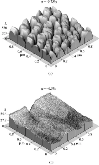
The surface analysis using atomic force microscopy shows a 3D-like columnar growth for samples with
ε = -0.75% and a planar growth for samples with ε = -0.5%, as shown in Figs. 6a and 6b, respectively. The planar surface is formed by two-dimensional layers with generation of steps with heights between 1 to 2 atomic monolayers (1ML ~ 0.293 nm). The columnar growth is formed by columns of 20 - 30 nm height with diameters ranging from 170 to 200 nm, randomly distributed over the crystal area, with a density of 4.5 x 109 cm-2. The shapes of surface features in this case do not resemble those of 3D islands commonly observed during Stranski-Krastanov growth12, indicating that the 3D growth occurred during the early steps of deposition. These results agree with the previous PL image observations and give additional evidence of the strong influence of the tensile strain on the crystal quality of InGaAsP layers.
Tensile and compressive strained In1-xGaxAsyP1-y/InP
MQW structures, of 10 periods (Nw) were grown with
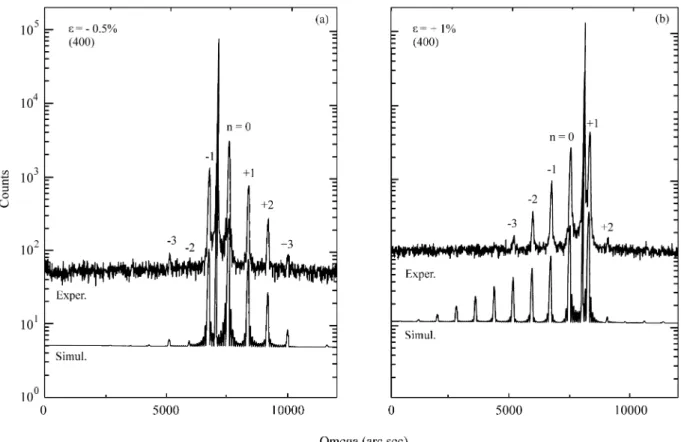
InGaAsP wells and InP barriers of nominal thicknesses of 8 nm and 4 nm, and 20 nm and 16 nm for tensile and compressive layers, respectively. All the samples analyzed here exhibited mirror-like surfaces. The simulated and ex-perimental X-ray diffraction patterns at the (400) reflection of the tensile and the compressive strained MQW In-GaAsP/InP structures, are shown in Fig. 7. The satellite peaks are narrow and strongly asymmetric due to the pres-ence of the biaxial strain. These peaks are shifted to the right side of the X-ray spectra main peak for tensile samples and to the left side for compressive ones. The X-ray FWHM of satellite peaks n = -1 and n = +1 are 80 arc sec for both samples. These results together with the observation of a large number of well-defined satellite peaks in the X-ray spectra clearly demonstrate the good crystalline quality of the strained layer MQW samples analyzed in this work. This is confirmed by the simulation of the X-ray data shown in Fig. 7, since no additional interfaces, composition vari-ations from layer to layer or period fluctuvari-ations were in-cluded in the kinematical model used13 to reproduce the experimental X-ray spectra. Photoluminescence measure-ments at T = 77 K on the same samples showed a PL linewidth of 26 meV and 18.8 meV for the tensile and the compressive strained samples, respectively. Despite that both structures exhibit a narrow and almost the same X-ray FWHM and mirror-like surfaces, the PL linewidth is larger for the tensile layer when compared to the compresive strained one. The above results suggest that the InP barrier layer smooths the InGaAsP/InP interfaces, but the
nary alloy still exhibits composition fluctuations giving rise to broad PL emission bands.
The last set of samples consisted of MQW structures with tensile (ε = -0.5%) quaternary barriers and compres-sive (ε = +1%) quaternary wells. The combination of strain and thickness values enables the growth of balanced struc-tures where the total strain is null. The net strain in these structures, known as zero net strain (ZNS), can be estimated using the following relation:
ε=εB tB +εW tW
tB + tW (1)
where, εi and ti are the strain and the thickness values,
respectively, of the barrier (b) and the well (W) materials. Three ZNS structures were grown at TG = 640 °C with
Nw = 2, 5 and 10 wells and nominal values of εb = -0.5%,
tb = 14 nm, εw = +1% and tw = 7 nm. The surface
morphol-ogy of the Nw = 10 sample was completely rough whereas
the two other structures exhibited mirror-like surfaces. The 77 K PL spectra of these MQW structures are shown in Fig. 8 and they consisted of two main emission bands: i) a high-energy emission with PL FWHM ranging from 13 to 17 meV, corresponding to the fundamental transition (e1-hh1) in the quantum well and ii) a broad band (labeled as B) at the low-energy side of the spectrum with PL FWHM ranging from 40 to 61 meV. The nature of the PL broad band-B will be addressed below. The insert of Fig. 8 shows the ratio between the integrated intensity of the fundamen-tal quantum well transition (IQW) and the broad band (IB)
as a function of the number of wells. The low-energy PL emission band dominates the spectra of ZNS structures with Nw = 5 and Nw = 10. The ZNS structure with Nw = 2 shows
an integrated intensity ratio that is about 10 and 30 times greater than samples grown with Nw = 5 and Nw = 10,
respectively.
The AFM 2 x 2 µm2 scans of Nw = 2, Nw = 5 and Nw = 10
wells ZNS heterostructures are shown in Fig. 9. The surface morphologies of the analyzed samples exhibited a clear dependence on the number of wells. For Nw = 2 the
mor-phology is almost flat with a very weak thickness anisot-ropy (Fig. 9a). For Nw = 5 the morphology shows an
anisotropic and modulated behavior, with a period of ~25 nm (Fig. 9b). A strong anisotropic thickness modula-tion occurs along the [011] direcmodula-tion, while no modulamodula-tion takes place along the direction [0-11]. It is also possible to observe in Fig. 9b some localized collapsed regions. A similar modulation and anisotropy were observed on sam-ples grown by gas GSMBE4. In the case of Nw = 10 the
surface is strongly irregular and also shows some degree of anisotropy (Fig. 9c). This structure exhibits a large thick-ness fluctuation with a shorter modulation period when compared to ZNS structures grown with Nw = 5. The above
results corroborate with those obtained with X-ray and the PL measurements and reveal the presence of interface undulations and/or composition variations in these struc-tures.
In order to study the effect of the growth temperature on the optical and structural properties of ZNS heterostruc-tures, an additional sample (Nw = 5) was grown at 670 °C.
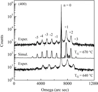
Figure 10 shows the X-ray diffraction patterns of two ZNS-structures (Nw = 5) grown at temperatures of 640 °C
and 670 °C. The X-ray simulation spectrum refers to the sample grown at 670 °C. The residual strain in both samples is lower than ε = ±0.01%. The X-ray pattern of the ZNS structure grown at 670 ºC (Fig. 10) exhibited narrower and more pronounced satellite peaks, when compared to the structure grown at 640 °C. The X-ray FWHM of n = +1 satellite peak is 180 arc sec and 380 arc sec for samples grown at 670 °C and 640 °C, respectively. The high X-ray
linewidth values observed for samples grown at low growth temperatures suggest the presence of interface undulations
and/or composition variations10 that strongly reduces the intensity and broadens the X-ray satellite peaks. In the case of InGaAsP/InP MQW structures (see Fig. 7) the InP barrier smoothes out all undulations at the InGaAsP surface and the interfaces are essentially flat5. However, InGaAsP/In-GaAsP-ZNS structures exhibit a pronounced undulation behavior as the number of well is increased giving rise to non-flat interfaces6,10,14,15.
The corresponding 77 K PL spectra of ZNS heterostruc-tures (Nw = 5) grown at 640 °C and 670 °C temperatures
are shown in Fig. 11. It can be clearly seen in this figure that the growth temperature strongly affects the PL spectra of ZNS structures. As the growth temperature increases from 640 °C to 670 °C the relative integrated intensity IQW/IB increases by almost an order of magnitude and the
PL linewidth is reduced from 16.7 meV to 11.4 meV, respectively. These results and those obtained from X-ray data shown in Fig. 10 suggest that the low energy emission PL band (B) is related to defects generated at the In-GaAsP/InGaAsP interfaces. When the growth temperature is increased from 640 °C to 670 °C the tensile strained InGaAsP layers are expected to experience reduced spino-dal decomposition effects, improving the crystalline quality of the quaternary interfaces.
Figure 7. Simulated and experimental X-ray diffraction pattern at (400) reflection of (a) tensile and (b) compressive strained MQW InGaAsP/InP structures.
Figure 8. Photoluminescence spectra at T = 77 K of MQW-ZNS struc-tures with 2, 5 and 10 wells. The insert shows the ratio between the integrated intensity of the fundamental quantum well transition (IQW) and
4. Conclusions
Strained InGaAsP/InP heterostructures grown by LP-MOVPE were analyzed using X-ray diffraction, photolu-minescence, photoluminescence microscopy imaging and atomic force microscopy. The obtained results revealed a strong influence of the strain in the optical, morphological and structural properties of the quaternary layers. Tensile InGaAsP layers show a broader PL linewith and rougher morphology when compared to compressive ones. The high linewidth values observed in the PL spectra of tensile
Figure 11. Photoluminescence spectra obtained at T = 77 K of ZNS structures with Nw = 5 and growth temperatures of 640 °C and 670 °C.
Figure 10. X-ray diffraction patterns of two ZNS-structures (Nw = 5)
grown at 640 °C and 670 °C. The X-ray simulation was carried out for the sample grown at 670 °C.
Figure 9. Atomic Force Microscopy of samples with (a) Nw = 2, (b) Nw
MQW structures were attributed to a high density of inter-face defects and/or composition fluctuations generated by the spinodal decomposition of the InGaAsP alloy. Strain compensated InGaAsP/InGaAsP-MQW structures exhib-ited a well-defined anisotropic surface morphology that is directly related to the number of wells and the growth temperature. Growth temperatures above 640 °C and a smaller number of wells reduce the strength of the low energy emission band bellow the fundamental quantum well emission peak observed in the PL spectra, and signifi-cantly improve the interface quality of ZNS heterostruc-tures.
Acknowldgments
This work was carried out under the contract P&D/DDR/150/97-TB between TELEBRAS R&D Center and Syncrotron Light National Laboratory from CNPq. The authors would like to acknowledge H. Gazetta Filho and Luiz. Carlos S. Vieira for the technical support.
References
1. Mathur, A.; Dapkus, P.D. IEEE Journal of Quantum Electronics, v. 32, n. 2, p. 222, 1996.
2. Otsuka N.; Kito, M.; Ishino, M.; Matsui, Y. Journal of Quantum Electronics, v. 32, n. 7, p. 1230, 1996. 3. Dong, J.; Ubukata, A.; Matsumoto, K. Jpn. Journal of
Applied Physics, v. 36, n. 9A, p. 5468, 1997. 4. Ponchet, A.; Rocher, A.; Emery, J.Y.; Starck, C.;
Goldstein, L. Journal of Applied Physics, v. 74, n. 6, p. 3778, 1993.
5. Goldman, R.S.; Feenstra, R.M.; Silfvenius, C.; Stal-nack, B.; Landgren, G. Journal of Vac. Sci. Technol. B, v. 15, n. 4, p. 1027, 1997.
6. Bangert, U.; Harvey, A.J.; Wilkinson, V.A.; Dieker, C.; Jowett, J.M.; Smith, A.D.; Perrin, S.D.; Gibbins, C.J. Journal of Crystal Growth, v. 132, p. 231, 1993. 7. Stringfellow, G.B. Journal of Electronic Materials, v.
11, n. 5, p. 903, 1982.
8. De Cremoux, B.; Hirtz, P.; Ricciardi, J. Inst. Phys. Conf. Ser., n. 56, p. 115, 1981.
9. Wang, T.Y.; Stringfellow, G.B. Journal of Applied Physics, v. 67, n. 1, p. 344, 1990.
10. La Pierre, R.R.; Okada, T.; Robinson, B.J.; Thompson, D.A.; Weatherly, G.C. Journal of Crystal Growth, v. 155, p. 1, 1995.
11. Zhou, X.; Charsley, P.; Smith, A.D.; Briggs, A.T.R. Inst. Phys. Conf. Ser., v. 138, p. 321, 1993.
12. Zangwill, A. Physics at Surface, chap. 16, p. 428-432, Cambridge University Press, Cambridge, UK, 1988. 13. Sperius, V.S. Journal Applied Physics, v. 52, n. 10, p.
6094, 1981.
14. Ponchet, A.; Le Corre, A.; Godefroy, A.; Salaün, S.; Poudoulec, A. Journal of Crystal Growth, v. 153, p. 71, 1995.