Universidade de Lisboa
Faculdade de Ciˆencias
Departamento de F´ısica
Electronics Design and Implementation of a
Compressed Sensing Instrument for Astronomy
Mestrado Integrado em Engenharia F´ısica
Raquel Bandarra Borges
Disserta¸c˜ao orientada por:
Prof. Dr. Andr´e Maria da Silva Dias Moitinho Almeida
Dr. Alberto Garcez de Oliveira Krone Martins
Abstract
Compressed sensing is a new concept that is attracting much research nowadays. The theory states that under certain conditions, only a relatively small number of samples need to be acquired for reconstructing an image or any signal in general [1]. In other words, compressed sensing enables signal compression at the acquisition stage. In contrast, with traditional methods the data is compressed after acquisition. An outstanding characteristic of compressed sensing (CS) is that signals can be reconstructed at sampling rates lower than those required in the framework of the Shannon-Nyquist sampling theory [2, 3].
This theory has been increasingly developed, in areas like computational mathematics, signal processing, among others [4]. Given that modern sensors are producing more and more in-formation, applications of CS start to appear in areas where data compression is an essential requirement. The most known early application is the Rice University single pixel camera [5]. Now, there are other instruments based on CS and applications to communications, medicine, astronomy and others research fields.
In this work we designed and implemented the electronic acquisition and control subsystems of a compressive imaging single pixel camera. The subsystem developed is composed of a Digital Micromirror Device (DMD) for coding the signal, a controller subsystem, an acquisition subsystem and a storage subsystem. These last two subsystems are integrated in a printed circuit board. The most important features of the system that we designed in this work is tahta it can provide good resolution with fast acquisition times, that it ensures synchronization between the modification of the signal encoding patterns and the signal acquisition, and that it is relatively a↵ordable and easy to reproductible.
The DMD is used for creating pseudorandom patterns that allows to encode an image with fewer samples than the image’s number of pixels. This camera uses only a single detection element, enabling the reduction of the complexity and the cost of the system. Similar systems can be used for high resolution imaging in wavelengths for which currently instruments are expensive, bulky or even impossible to build.
Keywords. Astronomy, compressed sensing, data acquisition, digital micromirror device, single-pixel camera.
Resumo
Aquisi¸c˜ao comprimida (tamb´em conhecida como compressed sensing) ´e um novo conceito que tem atra´ıdo muita investiga¸c˜ao nos dias de hoje. Esta teoria afirma que s´o ´e necess´ario adquirir um pequeno n´umero de medidas para reconstruir uma imagem ou qualquer outro sinal [1]. De outra forma, a aquisi¸c˜ao comprimida permite que a compress˜ao possa ser realizada durante a pr´opria obten¸c˜ao da imagem. Uma caracter´ıstica not´avel da aquisi¸c˜ao comprimida ´e que os sinais podem ser reconstru´ıdos com taxas de amostragens mais baixas que as impostas pela teoria da amostragem de Shannon-Nyquist [2, 3].
Esta teoria tem sido cada vez mais desenvolvida, tanto nos campos da matem´atica computa-cional como do processamento de sinal [4]. Dado que hoje em dia temos que armazenar cada vez mais informa¸c˜ao, tˆem come¸cado a aparecer aplica¸c˜oes onde a compress˜ao de dados ´e um requisito fundamental. Uma das aplica¸c˜oes mais conhecidas ´e a cˆamara de um pixel desenvolvida por investigadores da Universidade de Rice [5]. Agora h´a outros instrumentos baseados na aquisi¸c˜ao comprimida e tamb´em aplica¸c˜oes nas ´areas da comunica¸c˜ao, medicina, astronomia e outros campos de investiga¸c˜ao.
Neste trabalho foi projetada e implementada a parte eletr´onica de uma cˆamera de aquisi¸c˜ao comprimida de um s´o pixel. O subsistema desenvolvido ´e composto por um dispositivo digital de microespelhos (tamb´em conhecido por DMD - Digital Micromirror Device), para codificar o sinal, um subsistema de controlo, um subsistema de aqui¸c˜ao e um subsistema de armazena-mento. Estes dois ´ultimos subsistemas est˜ao integrados numa placa de circuito impresso. As caracter´ısticas mais importantes do sistema que desenvolvemos neste projecto s˜ao a possibil-idade de atingir boa resolu¸c˜ao om tempos de aquisi¸c˜ao r´apidos, o facto de que ele garante a sincroniza¸c˜ao entre a mudan¸ca de padr˜oes de modula¸c˜ao do sinal e a aquisi¸c˜ao do sinal, e que ele ´e relativamente acess´ıvel e facilmente reprodut´ıel.
O DMD ´e utilizado para executar padr˜oes pseudo-aleat´orios que permitem codificar uma im-agem com menos amostragens do que o n´umero de p´ıxeis dessa imagem. Esta cˆamara utiliza um ´unico elemento de detec¸c˜ao que permite reduzir tanto a complexidade como o custo deste sistema. Sistemas semelhantes podem ser usados para detectar com maior resolu¸c˜ao em com-primentos de onda para os quais os instrumentos de medida so caros, volumosos ou at´e mesmo imposs´ıveis de construir.
Palavras-Chave. Aquisi¸c˜ao comprimida, aquisi¸c˜ao de dados, astronomia, cˆamara de um pixel, dispositivo digital de microespelhos
Acknowledgements
First of all, I would like to thank my supervisors that guided me throughout this project. Prof. Doctor Andr´e Moitinho for making me work with him like two real engineers, because this is all about an engineering process. To Doctor Alberto Krone-Martins, thanks for showing me the real world of science and, of course, for his contributions.
To my master’s coordinator, I would like to thank for the support and for telling me I had the potential to do more.
All the people from the laboratory, where I had the opportunity to work, have here a special acknowledgement, because all together they create a great research/development environment, where is inspiring to work.
As this is a final work of my integrated master, I would like to thank my colleagues that became friends during all this years. A special mention goes to Rita, Rodrigo, Fraz˜ao and Gon¸calo. Each one has a special contribution for my growth as a student and mainly as a person. Thanks for the support.
My family was also fundamental as a supportive solid basis. They were great, understanding all the moments I had no time to spend with them and celebrating my victories with me.
And last, but not least, a special thank you Daniel for always be at my side discussing ideas and ideals, celebrating my achievements and also for never letting me give up.
Contents
Abstract ii Resumo iv Acknowledgements vi List of Figures ix Abbreviations xi 1 Introduction 11.1 Context and Motivation . . . 1
1.2 Traditional Imaging Framework . . . 3
1.3 Compressed Sensing . . . 3
1.4 Advantages of CS . . . 5
1.5 Applications of CS . . . 6
1.6 Document Roadmap . . . 8
2 Electronics of a Single Pixel Camera 9 2.1 Concept . . . 9 2.2 Detailed Design . . . 10 2.2.1 Photodiode . . . 10 2.2.2 Optical Modulator . . . 12 2.2.3 Acquisition System . . . 14 2.2.4 Storage System . . . 17 2.2.5 Control . . . 17 2.3 Procurement . . . 18 2.4 Implementation . . . 22 2.4.1 Acquisition System . . . 22 2.4.1.1 Photodiode . . . 22 2.4.1.2 Integrator . . . 22 2.4.1.3 Energy Sources . . . 25 2.4.1.4 A/D Converter . . . 27 2.4.2 Storage System . . . 32 2.4.3 Optical Modulator . . . 34
2.4.4 Printed Circuit Board . . . 38
2.4.5 Final Circuit and Control System . . . 41
3 Conclusions and Perspectives 45 3.1 Future Work . . . 46
A Parts and materials 49
A.1 List of materials . . . 49 A.2 Hardware . . . 50 A.3 Software . . . 50 B PCB and Schematics 53 C Programming codes 55 C.1 MATLAB Code . . . 55 C.2 Arduino Code . . . 59 Bibliography 65
List of Figures
2.1 Main execution flow of the system designed during this project. . . 9
2.2 Scheme of a PIN photodiode. Photodiodes are the preferred devices for high sensitivity and high speed at low cost. [26] . . . 11
2.3 Photosensitivity of the photodiode S1223 in the spectrum range [25]. . . 11
2.4 The Hamamatsu S1224 photodiode used in this project. . . 12
2.5 The DMD used in this project. . . 13
2.6 In a DMD, tilting micromirrors are responsible for the optical modulation. Adapted from [30] . . . 14
2.7 Schematics of the ICV102 integrator transimpedance amplifier [32]. . . 15
2.8 On the left is the IVC102 integrator and on the right is the LTC2440 ADC. . . 15
2.9 Block diagram of the ⌃ ADC [33]. . . 16
2.10 Procurement workflow. . . 19
2.11 Screen shot of the shopping page of Farnell. . . 20
2.12 Check list of some components. . . 21
2.13 Generated current (A) in order to luminosity. . . 22
2.14 Example of a breakout board with an IC soldered. . . 23
2.15 Schematics of the integrator in CadSoft EAGLEc. . . 23
2.16 Code section where the switches are controlled. . . 24
2.17 Reset and integration timing. Adapted from [32]. . . 25
2.18 Integrator’s voltage output vs di↵erent integration times. . . 26
2.19 Velleman’sc kit to built a power source. Before and after soldering components. 26 2.20 Power source and the adjacent coil. . . 27
2.21 Schematics of the ADC connections in the Fritzing software. . . 28
2.22 Setup part of the code to control the ADC. . . 29
2.23 Function SpiRead from the program to control the ADC (J. Beale) [49]. . . 30
2.24 Loop part of the code to control the ADC. . . 31
2.25 Comparison between the output value from the source and the digitalized value. 32 2.26 Setup part of the code to control the SD card. . . 33
2.27 Loop part of the code to control the SD card. . . 34
2.28 Initialization of the code to control both the DMD and the Arduino. . . 36
2.29 Code to generate the patterns that wil be sent to the DMD. . . 36
2.30 Code to filling the matrix of a RGB bitmap and to send the pattern to the DMD. 37 2.31 DLP disassemble - the before and after, respectively on the left and on the right. 37 2.32 Top (left) and bottom (right) layers of the printed circuit board. . . 38
2.33 Top layer of gerber file of the printed circuit board (real size board). . . 40
2.34 Bottom layer of gerber file of the printed circuit board (real size board). . . 40
2.35 Top and bottom layers of gerber file of the printed circuit board (real size board). 41 2.36 Breadboarding of the final circuit to be implemented in the PCB. . . 42
2.37 Comparison between the analogic and the digital signal from the acquisition. . 43
2.38 Code to perform the sampling process. . . 43
2.39 Code to talk to Arduino and control the signal acquisition. . . 43
2.40 Code in arduino to communicate with the ocntroller. . . 44
B.1 Top and bottom layers of gerber file of the printed circuit board. . . 53
Abbreviations
ADC Analog to Digital Converter BMP BitMaP
CMOS Complementary Metal-Oxide-Semiconductor CS Compressed Sensing
CSV Comma-Separeted Values DLP Digital Light Processing DMD Digital Micromirror Device
EAGLE Easily Applicable Graphical Layout Editor ESD ElectroStatic Discharge
FPGA Field Programmable Gate Array GND GrouND
HD High Definition IC Integrated Circuit
IDE Integrated Development Environment INL Integral NonLinearity
IP Internet Protocol IR Infra Red
I2C Inter-Integrated Circuit
LED Light Emitting Diode LF Line Feed
MATLAB MATrix LABoratory MISO Master Input Slave Output MOSI Master Output Slave Input PCB Printed Circuit Board PD PhotoDiode
PIN P-type Intrinsic N-type semiconductor RC Resistor-Capacitor
RGB Red Green Blue RMS Root Mean Square
RNDIS Remote Network Driver Interface Specification SCLK Serial CLocK
SD Secure Digital SDO Serial Data Output SDI Serial Data Input SMD Surface Mount Device
SOIC Small Outline Integrated Circuit SPI Serial Peripheral Interface SS Slave Select
SSOP Shrink Small Outline Package TCP Transmission-Control Protocol
TCP/IP Transmission-Control Protocol/Internet P rotocol TTL Transistor-Transistor Logic
UART Universal Asynchronous Receiver/Transmitter USB Universal Serial Bus
VCC Voltage Collector to Collector
WVGA Wide Video Graphics Array XOR eXclusive OR
Chapter 1
Introduction
1.1
Context and Motivation
Since ever, we humans try to reach the stars and many of the technology developed by hu-mankind is motivated by this inherent dream.
The observations and experiments are usually the first steps of the scientific method, so the humankind always tried to develop the best observation tools possible [6]. In Astronomy, however, one can only perform observations and hardly any experiment is possible: the objects of study are far away, and at least until now, completely out of the reach for in-situ experiments. Scientists need to work with telescopes and cameras to record images of the celestial bodies.
Nowadays, imaging with good resolution, sensibility and speed are easily accessible to the average user. However, in research and development environments, imagers must be at a higher level, usually with better features and certainly with much larger detection areas, thus producing each time more information [7]: we are now facing challenges at the Petabytes level, and in a few years, we are expected to cross the Exabyte scales.
Besides that, while consumer imaging devices operate in the optical wavelengths, Astronomy has wide interests in the infrared wavelengths (and also in other exotic regions of the electro-magnetic spectrum). Bodies in universe radiate in infrared (IR) ranges, and this region of the
spectrum allow us to probe through the dust, providing important astronomical information, for instance, about the birth of stars. Accordingly, it is important for Astronomy to have access to cameras with capability to detect IR emissions. This is, however, a feature that can quickly increase the cost and complexity of an instrument.
In recent years, an approach called compressed sensing1 emerged [1, 8], holding the promise
to solve both of the aforementioned challenges. One of the first proposed solutions of a real world application of this theory is to have a camera based on a single pixel detector instead of a detector array. Thereby, it would be only necessary to improve the features of a single pixel instead of a matrix of pixels.
The present work aims at designing and implementing the electronics subsystem of an a↵ord-able and simple, but widely flexible, camera based on the theory of compressed sensing (CS). This approach requires much less measurements than the number of pixels in the final image. The signal modulation is based on a Digital Micromirror Device (DMD) and the wavelength achievable is dependent on the characteristics of the chosen photodiode, that is used as a single pixel detector. To design and assemble the system, component by component, bring us the freedom to customize each of the instrument features.
Using only one photodiode instead of an usual pixel array allows to have a single-pixel camera and when upgrades are needed, it is only necessary to replace one pixel instead of an array of them, reducing the cost, the size and the complexity of the imaging device.
Also, compressed sensing theory is interesting because, unlike the traditional imaging frame-work, it compresses the signal during the acquisition stage. In the traditional model, it is necessary to have lots of memory space to store data, although some of that data will be useless after some compressing process. With CS, this can be avoided and one only need the memory space to the meaning data.
1In the literature this can also be refereed as compressive sensing, compressive sampling, compressed
3
1.2
Traditional Imaging Framework
Traditionally, imagining applications are based on the Shannon-Nyquist theorem. This theo-rem is, in fact, used in most real life signal processing acquisition applications. The Shannon-Nyquist theorem [2, 3], in terms of frequency, can be stated as: the sampling frequency should be at least twice the highest frequency contained in a bandwidth limited signal. In other words, this theorem states that the sampling rate should be higher than twice the bandwidth of the signal to be recovered [9].
The limitations of the traditional framework are that for some applications (e.g. applications needing to measure higher frequencies), much better acquisition hardware like ADCs with more bits of resolution are necessary. Also, in this framework, the compression of an image is only possible after all image acquisition is performed. However, as said in one of the seminal works of CS [1]: “Why go to so much e↵ort to acquire all the data when most of what we get will be thrown away? Can’t we just directly measure the part that won’t end up being thrown away?”. The solution is an imaging method using compressed sensing theory.
If an analog signal has a structure, it can be processed more efficiently than what is supposed with the Shannon-Nyquist theorem, since this theorem does not take the signal structure into account [4].
1.3
Compressed Sensing
Compressed sensing might become a revolutionary method to acquire and compress signals. Its only requirement is that the measured signal has some type of structure that can be represented in some basis [1, 8, 10, 11]. In this framework, the signal is represented by a measurement vector of length N where K measurements are nonzero, and where K ⌧ N. Thus the compression is naturally performed during the signal acquisition.
In order for CS to be possible, the signal has to be compressible or, in other words, it has to have a sparse structure in some basis. Therefore, sparsity is a fundamental concept in all CS related works. If a signal x is projected in some basis , the result is given by:
↵ = Tx
The signal x is called K-sparse in if there are only K⌧ N nonzero entries in the coefficient vector ↵. The non zero coefficients are those containing the significant information, and so one can obtain an efficiently approximation of signal x using only these significant coefficients. In fact, it has been shown in the literature that the recovery is exact under certain conditions [1, 8, 12].
During the measurement process only the values of these few coefficients must be preserved, so the measured signal will tend to be much smaller than the original signal. In the so called, non strict sparsity, one can consider the entries as zero when they are smaller than a certain threshold, and thus close to zero. This is the type of sparsity that is more likely happen in the real world, for instance, because of the added intrinsic noise from any measurement process.
In CS, the K significant coefficients of ↵ might not be measured directly. Rather, it is measured from M < N projections y of the signal on a new set of basis functions ✓, where M K. So, what is acquired is:
y = ✓x
After the signal acquisition, however, it is necessary to reconstruct the signal. There are exact and approximated solutions to this problem. Nevertheless, most of them are based on solving mathematical optimization problems. For instance, to solve an exact problem, one could use a minimization solution with a l1-norm optimization:
min↵||↵||l1 s.t. y = ✓⇤ ↵
Where ✓ is indexed by ⇤ since it forms a deterministic ensemble from a random selection of vectors from the basis ✓. Classical l2-norms can also be used, as well as more modern l0-norms.
It is possible to adopt more realistic models, considering the added noise to the equation and to the optimization constraints. In practical applications, this will be always the case.
5
Applying these methods, it is possible to obtain the value of x, performing the reconstruction of the signal. This reconstruction is only possible if the signal x is sparse in some representation, what is always the case for any signal of physical interest – only pure random noise will never be sparse in any basis.
1.4
Advantages of CS
The adoption of CS frameworks will likely allow the creation of systems capable of dealing with larger datasets with many more dimensions, and also performing faster data acquisition. They also enable instruments working on parts of the electromagnetic spectrum that were previously unreachable (like the single pixel THz imaging system [13] that explores an almost unreachable part of the electromagnetic spectrum).
Compressed sensing theory applied to imaging systems can o↵er some noteworthy features like universality, encryption, progressivity, computational asymmetry and scalability [5, 12]. Each of these features will be described below.
Random measurement basis are universal because they can be paired with any basis, so they can be used in any environment. This feature is also future-proof because if happens to be discovered a new sparsity basis, with the same acquired set of measurements it is possible to reconstruct the image with better quality.
CS imaging method can be seen as encryption because only who knows which pseudo-random projections were used can reconstruct the signal. To other observer, the measurements will look like noisy, meaningless data.
As measurements are random, they have equal priority in each one has more information, so they create a robust coding. This leads to a progressively better reconstruction each time a new measurement is added, improving the image quality. With this feature, the reconstruction survive even if some measurements were lost.
The computational asymmetry is about having the heaviest computational requirements in the decoder, letting the encoder relaxed, only having to compute the projections. This is
important because it is easier (and cheaper) to allocate resources to the decoder. In space instrumentation, this advantage have a special importance since the decoding step is performed by the ground segment, on Earth, where energy is usually not a problem.
Finally, it is possible to adaptively select how many measurement the system will compute, so the system is scalable. The bigger the number of measurements, the best the image quality. The trade o↵ to this image improvement is the acquisition time that also increases. But even with few measurements, depending on the sparsity of the signal, it is already possible to have images (without taking too long to acquire the image).
1.5
Applications of CS
With the advent of compressed sensing, real world applications started to appear in fields like imaging and communication systems [5, 14–18]. In the imaging area, the most explored fields were optics, signal processing, optimization and astronomy. In communications, CS is already part of the solution to some systems’ problems [17].
In this section, we will present some of the applications of compressed sensing and a brief description of each one.
The Rice single-pixel camera [5] was one of the first real world applications using compressed sensing and it is one of the main inspirations of this work. As the name says, this camera has only one pixel, so it means that it capture an image with a single detector. This imager uses a digital micromirror array to modulate the signal on a pseudorandom array, where the captured image is projected, before the combined intensity is measured by the detector. The CS optimization tools are finally applied in the image reconstruction process. One problem of this system is the time required to acquire the signal. During the integration the camera needs to be focused in the same object. It can be faster, but faster measurements increase the noise in each measurement, setting aside the possibility of video applications.
In Marcia et al. work [14] it is proposed a CS application using coded apertures, where if a coded aperture has a pseudorandom construction, the result will satisfy the Restricted
7
Isometry Property [19]. The structure of the resulting sensing matrix provides a speed rising relatively to common matrices, allowing fast computation. The random lens imaging [20] is an interesting architecture for practical and implementable compressive imaging because it capture all measurements at the same instance. So, it does not require a large and complex imaging assembly.
A random convolution step directly within CMOS electronics was been proposed in [21] and the main advantage is that the optics required in spatial light modulation step are removed, decreasing the imager size and lowering its cost. This architecture is very flexible because it could accept di↵erent basis and coefficients for the projection process.
A real time spectral imager was proposed in [15]. The idea is each pixel measurement is the coded projection of the spectrum in the corresponding spatial location in the data cube. This solves the trade o↵ that had to exist between spectral and spatial resolution, increasing the spectral imager’s performance.
Applied to biomedical imaging, CS was already implement in real life to fluorescence mi-croscopy [16]. The microscope built in that study was based on a dynamic structure wide-field illumination and a fast and sensitive single point detection. This allows the reconstruction of images of fluorescent cells and tissues using much lower sampling ratio than what was done until then, in other words, the number of pixels in the reconstructed image is much smaller than the number of measurements.
In communications systems, there are already several applications using compressed sensing theory as wireless channel estimation [22], network tomography [23], networked control [18], beside others. Hayashi et al. [17] made a survey where they present this applications. As wireless channels are sparse (channel’s sparsity is proportional to bandwidth), it is possible to make an estimation with less signals. Network tomography is used for estimations too, but in this case, link delays’ estimation. In network control, CS is basically used for signal compression because it has very tight rates of network used to the communication between the controller and the control plant.
Finally, CS based techniques may have important consequences and practical applications to astronomical studies in the future. One of these, and the only that was already tested in a real space mission, is the data compression characteristics of the CS measurements. As mentioned in the Introduction section of the present work, with the development of technology, Science is acquiring each time more data in ever shorter periods of time. In Bobin et al. [7], the authors propose a method for the transmission of astronomical images that is adapted to the Herschel space mission, using compressed sensing as coding-decoding architecture. The objective was to merge both the acquisition, compression and maybe one day the data processing system. In their paper, they proposed a method to perform the compression on board of the satellite and afterwards a new algorithm to solve the decoding problem as quickly and as accurate as possible.
1.6
Document Roadmap
This dissertation follows with a description of the conceptual design, detailed design, procure-ment, implementation and validation works that were performed towards the development of the electronics of a Single Pixel Camera. In sections 2.2 and 2.4, the camera description is divided in its several functional subsystems.
Finally the conclusions are presented in Chapter 3, including directions for future work and some ideas for improving the system.
Chapter 2
Electronics of a Single Pixel Camera
2.1
Concept
A single pixel camera based on CS is an imaging device that acquire an image using a single light sensitive element, thus naturally compressing the signal during the acquisition process. It relies on a single detection element and on some type of signal modulator.
Our single pixel camera concept is summarized in Fig. 2.1. There, we have the main compo-nents or subsystems of the electronics. The system is composed of a digital micromirror device (DMD) as optical modulator, a photodiode (PD) as single light detection element (pixel), an acquisition system that contains an integrator and an analog to digital converter (ADC), a storage device and finally a controller system.
Figure 2.1: Main execution flow of the system designed during this project.
Fig. 2.1, also shows the functional aspects of the concept. The system has two parallel flows. The red arrows follow the signal flow since its formation in the photodiode (PD) to the storage device and possible later reconstruction. The first small red arrow (leaving the PD) is a current signal, that is converted to a voltage signal and then to a digital signal in bits (second red arrow). Finally the storage device may send a signal to the controller indicating that the data is saved. The blue arrows are the commands from the controller that make the entire system to work.
Our main application of the single-pixel camera is for astronomy purposes, so it is relevant that the photodetector is sensible to infrared and/or visible light. In the signal acquisition from the photodetector, one has to assure that the signal has proper amplification to be read by an analog to digital converter (ADC). Also, an integration solution for low current values must be considered.
For the ADC component, the resolution and conversion speed are the most important charac-teristics. After having digitalized the signal, in order to be able to reconstruct the image at a later moment, a mechanism will be needed to store the digital data.
At the pattern generation component, it is important that the modulator provides the pos-sibility to project the signal over a large number of patterns. The higher the number of patterns, the best the final image resolution that can be obtained. Finally, a system to control this pattern generation and possibly the synchronization of all single-pixel camera elements is necessary.
2.2
Detailed Design
2.2.1 Photodiode
In the market today, a large variety of light detectors are available, for example: photodiodes, phototransistors, solar cells, photomultiplier tubes and charge-coupled devices (CCD) [24]. The latter is largely used in imaging, but in our specific case, we wanted a single pixel element
11
and opted for the photodiode, as our application requires only a single sensitive pixel, operating at low energy levels.
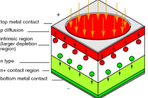
The photodiode adopted as the “single pixel” in this prototype is the Hamamatsu S1223 [25]. It is a PIN (P-Intrinsic-N) photodiode. It has a higher speed of current generation, because of the larger distance between P and N layers, than in common photodiodes.
Figure 2.2: Scheme of a PIN photodiode. Photodiodes are the preferred devices for high sensitivity and high speed at low cost. [26]
Figure 2.3: Photosensitivity of the photodiode S1223 in the spectrum range [25].
For this project a light detector is required that covers, at least the visible and and some infrared wavelengths. The photodiode also has to be sensitive to low luminosity (below ambient light). This photodiode fulfills the requirements of out project and it was also used in the Rice single-pixel camera project [5]. The photodiode choice defines the cameras wavelength range sensitivity. As mentioned before in this dissertation, our objective is to be able to capture light between infrared and visible range. Fig. 2.3 shows that the photo sensitivity of this photodiode and we can see that it has high sensitivity in the IR range (700 nm - 1 µm). The main features of the photodiode (shown in Fig. 2.4) are:
• High sensitivity in visible to near infrared range
• High reliability
• High-speed response: fc = 30 MHz
• Low capacitance
Figure 2.4: The Hamamatsu S1224 photodiode used in this project.
2.2.2 Optical Modulator
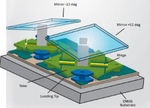
The component that allows the single pixel camera to modulate the signal, and thus to re-construct images with several pixels, is the Digital Micromirror Device (DMD). This device is a matrix of micromirrors that can be reconfigured, and thus each micromirror can reflect the light inside or outside a certain optical system. Thus, the DMD allows the creation of a multitude of patterns for encoding samples of an image for later reconstruction.
This component is an essential part of many devices in modern display technology, from projectors [27] to HD televisions [28, 29].
The DMD used in this work is a component of a Texas Instruments developers kit: the DLP LightCrafter Evaluation Module [27]. This kit is the basis of a common light projector and was created for facilitating research on the use, and the integration of, DMDs in industrial, medical and scientific applications.
Some of DLP3000 DLP 0.3 WVGA DMD main features are:
13
• 608 ⇥ 684 Array of Aluminum, Micrometer-Sized Mirrors O↵ering up to WVGA Reso-lution (854⇥ 480) Wide Aspect Ratio Display
• 7.6 µm Micromirror Pitch
• ±12 Micromirror Tilt Angle (Relative to Flat State)
• 5 µs Micromirror Crossover Time
• Highly Efficient in Visible Light (420 to 700 nm)
• Low Power Consumption at 200 mW (Typical)
• Dedicated DLPC300 Controller for Reliable Operation
• Supports High-Speed Pattern Rates of 4000 Hz (Binary) and 120 Hz (8-Bit)
• 15-Bit, Double Data Rate (DDR) Input Data Bus
• Integrated Micromirror Driver Circuitry
• Supports 0 C to 70 C
Figure 2.5: The DMD used in this project.
The resolution, the power consumption and the speed available are suitable to this single-pixel camera project. Associated with a good quality-price relation, this Texas Instruments kit was the best choice for the present prototype.
Each micromirror of the DMD is controlled separately and has two positions (+12 and 12 ). With an opto-mechanics system coupled, only one of the positions of the micromirrors will reflect the light into the detector, enabling the measurement of the signal projected on each pattern.
Figure 2.6: In a DMD, tilting micromirrors are responsible for the optical modulation. Adapted from [30]
2.2.3 Acquisition System
The acquisition system is composed by: a precision integrating amplifier IVC102 to amplify and convert the photodiode signal from current to tension; a 24-bit analog-to-digital converter LTC2440 to convert the integrated analog signal in tension to a digital signal in bytes; and a microcontroller Arduino [31] to control the integration and reset time of the IVC102 and to allow the A/D conversion by the LTC2440.
An integrator is an op amp circuit that generates a voltage proportional to the magnitude and duration of a certain input voltage with respect to a reference voltage, usually 0 V , the ground. A transimpedance amplifier is a circuit that amplifies the signal, converting it from current to voltage. The present project requires a component that performs all these functions: convert the signal from the PD from current to voltage, accumulate it and amplify it.
Among the di↵erent solutions available in the market, we selected the IVC102 from Texas Instruments/Burr-Brown Corporation. The IVC102 is a precision switched integrator tran-simpedance amplifier. It has an op amp to amplify and transform the current signal into voltage signal, and capacitors to integrate the signal. Our choice was motivated by the fact that it is a fast integrator and a lower noise in comparison to conventional transimpedance op amp circuits that require a very high value feedback resistor. One of its main applications in the literature [32] is precision low current measurements, exactly the case of a photodiode.
Its main features are:
15
• Gain programmed by timing
• Low input bias current: 750 fA max
• Low noise
• Low switch charge injection
• Fast pulse integration
• Low nonlinearity: 0.005 % typ.
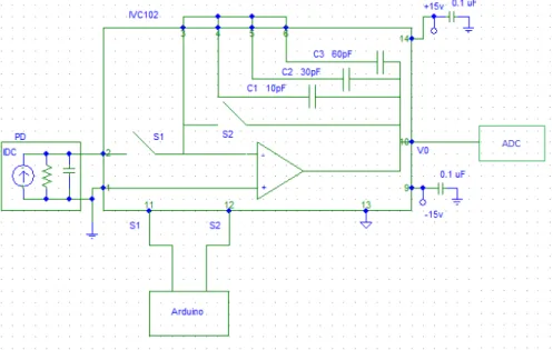
Figure 2.7: Schematics of the ICV102 integrator transimpedance amplifier [32].
From Fig. 2.7 we can understand the working process of this component. When the S1 (switch 1) is closed (low ) and S2 is open, the circuit start to integrate, accumulating signal in the capacitors. At some point, an order is given to S1 to open and the integrated signal is ready to be acquired. After the acquisition, S2 is closed and quickly open, resetting the system. To restart the process, S1 may be closed again.
Figure 2.8: On the left is the IVC102 integrator and on the right is the LTC2440 ADC.
An ADC (analog to digital converter) is a component that converts an analog signal to a digital signal. The conversion technology delta-sigma, or ⌃, is one of the most advanced
techniques. It produces a slope voltage in the output of the ADC when the input voltage is connected to the ADC input. Then this ramp is compared, using a comparator, to the ground voltage, acting like an 1 bit ADC. The output of the comparator is latched through a flip-flop D and the output returns to the start, making the feedback of the system and trying to take the integrator to have a 0 V output. The output in bits is ready after the signal passes the flip-flop. In Fig. 2.9 the schematics of the ⌃ ADC operation can be found.
Figure 2.9: Block diagram of the ⌃ ADC [33].
The ADC choice was driven by the speed of convertion and resolution in bits. After knowing that a fast method to digitalize a signal is the di↵erential ⌃ method, it also become a keyword to look for. The Linear Technology LTC2440 ADC corresponds to the requirements, being a 24 bit high speed di↵erential ⌃ ADC with selectable speed and resolution. One of the main applications of this ADC indicated by its datasheet [34] is high speed data acquisition. This component can connect to a microcontroller via SPI (serial port interface), thus simplifying its usage in complex projects.
Its main features are:
• Selectable speed/resolution
• 2 µV RMS Noise at 880 Hz output rate
• 200 nV RMS noise at 6.9 Hz output rate with simultaneous 50/60 Hz rejection
• 0.0005 % INL, no missing codes
• Autosleep enables 20 µA operation at 6.9 Hz
17
• Di↵erential input and di↵erential reference with GND to VCC common mode range
• No Latency, each conversion is accurate even after an input step
• Internal oscillator no external components
2.2.4 Storage System
The data flow from the ADC is stored on a 2 GB MicroSD memory card. The recording system used a break out board Stackable SD Card shield V3.0 from Adafruit that is compatible with the Arduino and the ADC via several interfaces: UART, I2C or SPI. After storing the data,
the signal can then be reconstructed with a computer.
Some features:
• Onboard 5 V > 3 V regulator provides 150 mA for power-hungry cards.
• Uses a proper lever shifting chip, not resistors: less problems, and faster read/write access.
• Push-push socket with card slightly over the edge of the PCB so it is easy to insert and remove.
• Simplified operation with Arduinos, with abundant literature examples (to see some examples: [35, 36]).
2.2.5 Control
To control the di↵erent parts of the single pixel camera, we used an Arduino Uno [31] and its open source Arduino Software (IDE). This software is based on Processing (an open source software, that uses a language similar to C) although the Arduino’s IDE is written in Java.
The Arduino is an inexpensive microcontroller for prototyping that can read inputs and gen-erate outputs. All this is possible by programming instructions in its dedicated software and connecting the Arduino pins toother electronics components, such as sensors or actuators. It
has analog and digital inputs/outputs, a power jack, a USB connection and it can communicate with other microcontrollers via UART TTL (5 V ) serial communication, SPI and I2C.
Algorithm 1 Pseudocode to control a single pixel camera using compressed sensing.
Require: k - number of measurements, M - pattern matrix, acquistiontime - time between the acquisition start and stop, changingtime - time the DMD is changing
Ensure:
1: while i < k do
2: savedtime1 currentime
3: if currentime > (savedtime1 + changingtime) then
4: AcqControl High
5: savedtime2 currentime
6: if currentime > (savedtime2 + acquistiontime) then
7: AcqControl Low
8: Signal read ADC
9: write the Signal in Memory Storage
10: nextpattern read next M line
11: send nextpattern to DMD
The pseudo code presented in Algorithm 1 shows how the measurement process is performed. In our project, it begins with a declaration of the number of measurements we want to make (k), and loops until that number is achieved.
Inside the loop there are four control parts. The first is related to integrator’s working process. To control the switches S1 and S2, refered in subsection 2.2.3, we have to code the functions presented in line 1-7 in Algorithm 1. It defines the start and stop of the integrator, establishing the acquisition/integration time. In line 8 of the same algorithm, there is the function to convert the signal from analog to digital. And in the next line, it is indicated that we have to save the digital signal that came from the ADC. The last control part is about the patterns of the DMD and when we have to change them to start a new measurement.
2.3
Procurement
Procurement is a very important phase of any project. Within the instrument requirements and budget constraints, one has to choose the best components possible and define priorities.
19
Although deserving a separate section in this dissertation, procurement is unavoidably an iterative process involving options in the detailed design and sometimes even in the conceptual design phase.
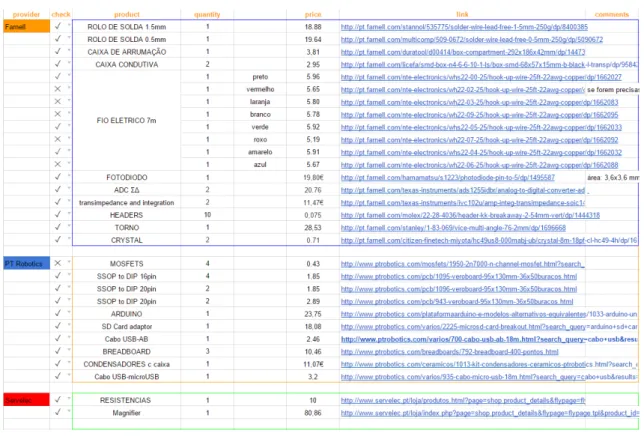
Finding the right components can be an hard task. It is important to check di↵erent providers if they have the products we are looking for, the prices, expedition time and, in the case of certain components, export restrictions.
Figure 2.10: Procurement workflow.
The workflow in Fig. 2.10 summarizes the procurement process from searching for the com-ponent to the testing and validation of it.
Once the general characteristics of each component are established, the search can start. A first triage starts by searching in the internet for components which satisfy our expectations.
The search focuses mainly on known electronics and optics companies like Texas Instruments [37], Thorlabs [38], Hamamatsu [39], Analog Devices [40], Linear Technology [34], Robert Mauser [41], Arduino [31] and some others.
Figure 2.11: Screen shot of the shopping page of Farnell.
After examining data sheets and finding components of interest, we look for them in some providers. There are many electronics/optics providers. We often select Farnell [42] because it is a well known high service distributor of technology products with a large variety, competitive prices and great delivery time (unfortunatelly, these products are always coming from foreign countries). We occasionally relied on a few portuguese eletronics shops, like PTRobotics [43], Servelec [44] and Inmotion [45], for some orders.
The next step is the validation of the choices by the MSc dissertation advisors. We have meetings where the choices are presented and justified. When agreement on components is reached, it passes to the order phase. If, for some technical or budget reason, the component is not approved, the process returns to phase one: research.
Before ordering the products, we have to confirm each one to be sure that we are selecting the correct component (sometimes, one letter in the name can change important characteristics
21
like surface-mount device vs. through-hole or a normal vs. a military component), check if the quantities are right and if the availability is still the same or at least not longer.
Figure 2.12: Check list of some components.
When the order arrives, it is important to make a check list to identify the items that were already received and the ones who are yet to come (example in Fig. 2.12). After receiving, we tested the components to ensure they meet the requirements announced. If everything is all right, it will be approved, but in other hand if some component did not come as intended, a complaint is send to the provider and the product is returned and replaced for the right one.
The procurement is finished when everything is approved and all components are ready to use, allowing to start the implementation phase. In practise, the procurement is considered also after the implementation’s start, whether for new components (and we had to update the detailed design too) or for places, for example a supplier to produce the printed circuit board (PCB).
2.4
Implementation
2.4.1 Acquisition System
2.4.1.1 Photodiode
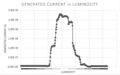
To confirm that the photodiode generates more current when the luminosity is higher, a luminosity response test was done. The photodiode started covered, then was slowly uncovered, getting full access to the ambient light and it was approached to a light bulb. Finally, ther reverse process was also performed. The generated current is shown in Fig. 2.13. The minimum generated current was not 0 A, confirming that this photodiode is sensible to IR light.
Figure 2.13: Generated current (A) in order to luminosity.
2.4.1.2 Integrator
The first action for the implementation of the IVC102 based integrator is to solder it to a breakout board in order to be able to use this SMD component in a breadboard. A breakout board is a board with a determined number of lines connecting the soldered component to pins (Fig. 2.14). That is used, for example to provide easy access to SMD components, transforming SMD components (or a complete electronic system like the microSD breakout board we will use in the storage system) into through-hole components and enable the connection between that type of components and a breadboard.
23
After soldering, it is very important to verify all the connections. We used the multimeter continuity option, in which the multimeter gives the resistance value between two connections (and beeps if they really are connected). If the multimeter indicates OP EN , there are no short circuits among the connections checked, the resistance is infinite between the two connections. In case the user do not want a certain connection but it was incorrectly done, there are solutions to this problem. Among the several solutions, the ones we used were: a desoldering vacuum pump solder removal tool (“solder sucker”) and a desoldering braid solder remover copper wick (“solder wick”).
Figure 2.14: Example of a breakout board with an IC soldered.
The integrator transimpedance amplifier has to be connected to the photodiode, the ADC, the Arduino, the ground and finally to a power source. Fig. 2.15 illustrates these connections in the schematics.
Figure 2.15: Schematics of the integrator in CadSoft EAGLEc.
Pin 1 is the connection to the analog ground. The 2nd pin is connecting the PD to the op amp allowing the integrator to receive the current signal. All the capacitors in this integrated
circuit (IC) are connected in parallel among them, creating a larger capacitor. The integrator has these three capacitors in order to enable a choice of di↵erent combinations of capacitors’ values. The user can also add more capacitors as we actually did. The e↵ect is to increase the charging time for a given voltage (signal), thus allowing the acquisition of stronger signals without reaching saturation too quickly. There are two pins with no internal connection and we can just connect them to ground for lowest noise. Pin 10 is the output and it is connected to the ADC. Pin 11 to 13 are the digital pins, in which pins 11 and 12 are wiring the switches to the Arduino and pin 13 is the digital ground. Finally, the pins which power the integrator are pins 9 and 14, giving the -15 V and +15 V , respectively. The capacitors near the power sources are bypass capacitors and their function is to avoid voltage peaks to enter in the IC, making the voltage signal more stable.
In order to allow a visible control of the switching process, we set two LEDs, one in each switch. Each LED is turned on when the correspondent switch is closed, or in digital words, when it is HIGH.
The switch control programming code we wrote is presented in Fig. 2.16. We have translated the logic shown in Fig. 2.17 into Arduino code.
25
In the setup we have declared the variables S1 and S2 as outputs, for the pins of the Arduino associated to the switches can send logic signals to the integrator. In the loop section we used the function digitalW rite to send the signal to each switch, creating an integration cycle. In the Detailed Design section we have explained in detail the e↵ect on the integrator of the logic here implemented. As commented in the code, we implemented several delay functions that are used to make the program wait a certain time. This is done in order to guarantee the proper sequential running of the integration’s phases: reset, pre-integration hold, integration and integration hold. The ADC code and the SDCARD code come after this last phase to acquire the signal, convert it and save it to a memory card.
Figure 2.17: Reset and integration timing. Adapted from [32].
After having the integrator implementation in place, several tests were made. The Fig. 2.18 shows the output from the integrator considering di↵erent integration times. In the first period of time (0 to 100 s) the integration time was 100 ms and then it grows with a factor of 10. Between 200 and 350 s, the integration time was 10000 ms and it has no saturation like in the last case with 100000 ms, and it already had a good enough signal amplitude to work with. This experiment was made with a 68µF capacitor. If we used a bigger capacitor, the output signal would have a smaller amplitude.
2.4.1.3 Energy Sources
Some type of power supply is necessary in all electronic equipment. To power the integrator, it needs -15 V and +15 V , and thus we had to have one power supply meeting these requirements. The K8042 kit [46] is a low cost symmetric 1 A power supply kit that goes from 1,2 V to 24
Figure 2.18: Integrator’s voltage output vs di↵erent integration times.
V , both positive and negative, which can generate the required voltage while being able to handle the need power for the circuit.
Figure 2.19: Velleman’sc kit to built a power source. Before and after soldering components.
To be easier to integrate in a future full design, we opted for a power source kit that has to be mounted and came without any box or button. Accordingly, we had to perform some soldering work of which the final result is shown in Fig. 2.19. To connect the kit to electricity, a coil was added and connected to the kit’s terminal blocks. In order to choose the intended voltage, the kit has two voltage regulators associated with two potentiometers. This kit generates a virtual ground in the middle of the two voltage regulators connected in series.
To power the ADC we need a 5 V source. So our idea was to create this source from the±15 V power source. We adopted one LM1086 5 V 1,5 A Dropout Positive Regulator [47] regulator and connect it with the +15 V and ground of the original source. It is very important to have all grounds connected, thus we can assure they are all at the same voltage level.
27
Figure 2.20: Power source and the adjacent coil.
2.4.1.4 A/D Converter
The LTC2440 ADC also needed to be soldered to a breakout board. This SMD component has a shrink small outline package (SSOP) package and that means the space between pins is only 0,635 mm against the 1,27 mm of the SOIC package of the integrator component. This makes the soldering work much more challenging. We had to be very precise and we had to adopt a technique in which we make a solder ball in the soldering iron and then fill both the IC’s terminals and the surfaces where we want to solder to. Then we align the IC with the surfaces to solder and with the iron we only warm up the solder at the surface and push it against the terminal. It is a good idea to start with two diagonal pins to ensure that the IC will be aligned. If for some reason some solder gets stuck between the terminals, we can just make a solder ball and roll it by the terminals and the gripped solder will fuse with the solder ball and let the terminals clean.
This component has 4 ground pins all internally connected to improve the ground current flow. They should all be connected to the same ground to work properly. The pins’ numbers are 1, 8, 9 and 16. The pins 10, 14 and 15 were not used so we connected them also to ground to avoid noise e↵ects.
As explained above, it is important to use bypass capacitors in connections to the power supplies. So, the VCC pin was linked with two capacitors (the values of the capacitors are
Figure 2.21: Schematics of the ADC connections in the Fritzing software.
be connected to a voltage value greater than 0 V and equal or smaller than 5 V (value of the VCC), so we chose the greater value, 5 V to allow a larger input (we will see later why).
To limit the high-frequency noise in the reference pins we put an RC filter (composed of two resistors and three capacitors) between the voltage supply and the pins.
The input pins allow us to receive the voltage signal from the integrator. Pin 6 is connected to ground as reference and pin 5 links the ADC with the integrator. Since the minimum input voltage for the ADC is -0,3 V we have to introduce an voltage o↵set to the circuit. So we add a voltage divider connected to the integrator and to a 5 V source and we o↵set the input in +5 V . But the maximum input voltage had also a limit, half of the reference voltage value, i.e. -2,5 V (if the pin 6 is grounded like in our case). To ensure that no signal above that value could pass, we add a 2,5 V zener diode as voltage limiter, that only let pass through it voltages under its characteristic value. We note that this component can influence the linearity of the acquisition, in which case it must be taken into account in the signal post processing.
Finally, there are four digital pins and they are essential for using SPI communication.
SPI, a protocol developed by Motorola [48], is an interface specification used for short distance communication between devices such as this ADC, an SD card and a master like a computer or an Arduino, for example. The SPI protocol needs four signals to be able to establish the communication: MOSI, MISO, SCLK and SS (also called SDI, SDO, SCLK and CS,
29
respectively in case of a slave device). The function of each pin will be explained below in our current case study: the ADC connection with Arduino.
The pin 13 is the SCLK pin and it is used to synchronize the data transfer, in which each bit is shifted out from the SDO pin in the falling edge of the clock. SDO or MISO pin is an input to the master and simultaneously an output to the slave device. In the ADC, SDO is pin 12 and it provides the result of the last conversion as a serial bit stream. In opposition, pin 7 is the SDI or MOSI and it is an output to the master and an input to the slave. This pin in the LTC2440 is used to select the speed and resolution of the output. The slave select pin (SS or CS) is an input to the slave and it is located in pin 11 in this ADC. This pin allows the master to select with which slave it wants to communicate, if it is linked to more than one slave as in our case (we have both ADC and SD card connected to Arduino via SPI). In Arduino, the SPI pins have specific positions, exactly named as MOSI, MISO and SCLK, except the SS that can be declared in the code with any other number of the available Arduino’s pins.
Figure 2.22: Setup part of the code to control the ADC.
To program the communication between the ADC and the Arduino via SPI, we had to include the SPI library in the code and to create a function to enable the reading from SPI bus. In
Fig. 2.22, the first line is the code for including the library. Fig. 2.23 shows the SpiRead function.
In the setup, we use the Chip Select (CS) to select with which device we want to communicate. When we set the pin associated to the CS of the ADC to LOW (variable CS ADC in the code), the communication via with the Arduino is open. Then we initialize the SPI and set its parameters using the functions of its dedicated library (the four lines with SPI.f unction()). An example is the function SPI.setBitOrder(M SBF IRST ) that forces the most significant bit to come always first. The Serial.f unction() are functions related to the serial monitor that exists inside the Arduino software and allow us to inspect immediate outcomes. In the final step, we have to turn HIGH the CS ADC to free the SPI bus, so that a new device can use the bus to communicate with the Arduino (the memory card board in our case).
Figure 2.23: Function SpiRead from the program to control the ADC (J. Beale) [49].
The SpiRead(void) built function uses another function, the SPI.transf er that allows the devices to send and receive data. The first function was built to read the 4 bytes sent by the ADC (as documented in the datasheet [33]). So, the reading process starts assigning the first value from SPI.transf er to the variable b, then assign the value of b to the result, shifted 8 bits. After this, the variable b receives the next byte and that value is added to the previous
31
result value, through the operator OR (represented by |= ). This process is repeated until the 4 bytes are read.
Figure 2.24: Loop part of the code to control the ADC.
Inside the loop, we had to change the ADC’s chip select again to LOW to enable the com-munication with the Arduino via SPI, as explained before. Then we inserted a f or cycle that makes the ADC acquire a certain number of readings (set by the nsamples variable) before sending the final result to the Arduino. Inside the f or loop we used the SpiRead function already described and set some rounding to the bytes acquired. After freeing the SPI bus, we have the variable volts where the data acquired is processed, su↵ering some conversions. To print in the serial monitor the values acquired, we used the Serial.print() that receives the defined variables sum (in bits), mins (in minutes) and volts (in volts). Later when the data will be saved in the memory card, the generated CSV file generated will look like a table.
the SD card matches the ADC’s input value, the values obtained were plotted in the graph presented at the Fig. 2.25. They always had the same value up to 1,25 V because it is half the voltage reference value used (Vref = 2,5 V in this case) and the ADC only converts values
from Vref
2 to Vref
2 . These results indicate that there is a good agreement between the data
acquisitions.
Figure 2.25: Comparison between the output value from the source and the digitalized value.
2.4.2 Storage System
In the SD card board we only had to solder the headers to be able to set the board on the breadboard with the rest of the circuit.
The connections between the SD card board and the Arduino were the SPI pins MOSI, MISO, SCLK and CS (the CS pin was assigned to Arduino’s pin 10) and the a connection to a 5 V power supply.
In the code for the SD card shown in Fig. 2.26, we included the SD dedicated library SD.h, that allows us to use several functions related to the SD card. In the second line the variable type created is File and we can read and write on it. Inside the setup, we started as usual to declare the pin, which connects the CS between the SD card board and the Arduino, as
33
Figure 2.26: Setup part of the code to control the SD card.
output and then turn that pin HIGH as we should always do to set free the SPI’s bus before any device wants to communicate.
After that, we initialize the SD card, printing in the serial monitor the status information about the process (for example: “InitializingSDcard...”). We used an if statement to check if the initialization was successful or not. If it failed, the program returns to the setup and continues to the loop (without saving anything to the SDcard).
Using the function SD.open we open a CSV file in writing mode (using the F ILE W RIT E parameter). Then, with the file opened, the code inside the second if statement prints some status information in the serial monitor, prints the headers T ime and V olt in the CSV file and finally close the file. In case of the if statement to be false, a error message appears in the serial monitor.
Figure 2.27: Loop part of the code to control the SD card.
Inside the loop code we opened the CSV file again to write the values acquired by the ADC. Those values are in the variables volts and mins that were described in the ADC’s subsection. It is important to print a comma between the values (writing myF ile.print(“, ”)) because the CSV (Comma-Separated Values) file, as the name indicates, separate the value fields with a comma between them. In the end we close the file and a done status information is printed in the serial monitor. Again, if the file does not open correctly, an error message is shown.
2.4.3 Optical Modulator
The DMD is controlled by a computer via Universal Serial Bus (USB), using a Transmission Control Protocol (TCP) connection. TCP is a very reliable transmission control protocol that allows the communication between entities (most commonly over an Internet Protocol - IP network). We had to configure the serial port where the DMD was connected to use Remote Network Driver Interface Specification - RNDIS drivers. This provides a virtual ethernet link to the DMD. RNDIS is Microsoft proprietary network protocol to use mostly in top of USB to create a virtual ethernet link between devices.
35
We used the MATLAB environment [50] to develop a program to control the DMD and the Arduino connected to the system. A key point is to synchronize these two devices in the main system loop, so they can work as a single entity. The code to control the devices relies on functions written by Jan Winter [51] to control the DMD.
In Fig. 2.28, we show the main function GeneratePatterns that returns a matrix samplingMat with the information used to generate the patterns. This function receive as arguments: the integration time (intTime), that will be send to the Arduino and used inside the acquisition code; the number of patterns to send to the DMD (nPatterns); the number of samples (nSam-ples) that allows to choose the size of the matrix (nSamples x nSam(nSam-ples); and finally the amplification factor (gFactor) that defines, in other words, the number of micromirrors used by each sample (gFactor x gFactor).
To initialize the connection with Arduino we used the function serial in line 61 to create a serial port object, in this case called arduino. This function defines COM6 as the port where the object will be connected and the baud rate as 9600 bps. In the next line we connect this object to the device using the fopen() function and in line 64 we set the terminator of the arduino serial object to LF (Line Feed), which defines that a message ends when this character is found. To initialize the DMD we create a TCP/IP object and define the DMD’s IP and its port.
The LightCrafter() function in line 70 was created by Jan Winter to allow MATLAB programs to talk to the device.
The piece of code in Fig. 2.29 shows the generation of the sampling matrix using the hadamard(n) function which returns the Hadamard matrix of order n.1 We set this order number as the total number of pixels. After normalization, in line 81 we convert the constant matrix hadSamplingMat into a numeric object samplingMat using the function double(). The imHad matrix is defined as a 3D matrix of zeros, in which one dimension will allow to have the RGB model. We use the disp to display some status messages to the user. To save the matrices created to use in future reconstruction of the image, we used the dlmwrite function, indicating
1A Hadamard matrix is a square matrix formed by
± 1 entries, with rows that are mutually orthogonal. We note that our system can adopt any ohter type of matrix and Hadamard was adopted only for quick convenience.
Figure 2.28: Initialization of the code to control both the DMD and the Arduino.
the directory of the file where to save, the object to save and which separator character we want to use.
Figure 2.29: Code to generate the patterns that wil be sent to the DMD.
In the DMD pattern part code of the sampling process in Fig. 2.30, it is described the filling of the 3D matrix of a RGB bitmap using loops that fill all the matrix’s elements, from the one in first line, first column to the last in the position [dmdX][dmdY], that are the size of the DMD (lines 108-118). To do so, it is necessary to reshape each line of the Hadamard matrix as a 2D matrix that will be used to configure the positions of the DMD micromirrors.
Then, in lines 122-126 is the code to send the patterns to the DMD, where first we create a BMP file with the imwrite function and save the imHad matrix we have just filled. The next step is to open that file and read it with the functions fopen and fread. The file could have a size infinite (argument inf ), with an uchar precision (8 bits). After close the file, we used the
37
setBMPImage function of the created class L to send the imDataHad matrix to the tcpObject, the DMD.
Figure 2.30: Code to filling the matrix of a RGB bitmap and to send the pattern to the DMD.
The DMD came integrated in the DLP LightCrafter and is mounted for being used as a projector. In order to use the DMD itself, and not as a projecter, we had to disassemble the optical module and expose the DMD and its controller. This work had to be done very carefully so as not to harm the DMD since it is a very sensitive device. In Fig. 2.31, we have the DLP in its original assembly in the left. There, the DMD is hidden behind the optical part. In the image on the right the DMD is already exposed and all the lens’ system was removed.
Figure 2.31: DLP disassemble - the before and after, respectively on the left and on the right.
2.4.4 Printed Circuit Board
Finally, the circuit should be moved from the breadboard to a printed circuit board (PCB) where each component is soldered to the PCB. This ensures that the connections are well connected, allows the circuit to be more compact, robust and transportable.
To design the PCB we used the Fritzing software [52] that allows to create a PCB with two layers. As we have made the schematics in the same software program, the components appear in the PCB window (in red the board of Fig. 2.32) and we had to put them in the places we want and design non overlapping routes.
Making a ground fill (light yellow in Fig. 2.32), where all the board is grounded except the places that have routes passing by, allows to do not have many routes that only will complicate the routing system and that might also increase the noise. The routes in the top layer are represented in yellow in left of Fig. 2.32 and the routes in the bottom layer are represented in orange in the right of Fig. 2.32. To connect the routes from one layer to another, there are vias, conductive holes, that go through the board across its thickness.
We manually designed all the routes, because the auto-route function was not reliable: over-flows and software crashes, were frequent when using this tool.
Figure 2.32: Top (left) and bottom (right) layers of the printed circuit board.
This PCB houses almost all the circuit designed in this work. It has both the integrator and the ADC, the photodiode, the SD card board, the 5 V source and some resistor, capacitors and a zener diode. The board also has connectors to the ± 15 V source and to the Arduino
39
board. With all these components it is important to think about placing optimization. The components should not be very close to avoid short circuits and to facilitate the soldering work, but in other hand they should be close enough to minimize the size of the routes. The components that will connect with other external components or are likely to be accessed should be near the borders to make easier the access to them, like the± 15 V sources.
The PCB is compact with 80 x 73 mm and that is another reason to keep it organized and in a way that is possible to understand what is the role of each component. The legends should be readable and if it is possible have the same orientation. It is important to take care not to place the legends above the routes. The components’ size are dependent of the board’s size and it could determinate if they should have though-hole ou SMD packages. In this board both options are available, so we chose the first one because it is easier to manually solder. The symmetry arrangement of the components is also important to the board organization as to give a better appearance in general and also because aesthetics are a good proxy to carefully designed systems.
To analyse and then order the PCB, we had to export the file to a gerber format, that is the standard image file format used by industry to describe the PCB images (copper layers, mask layers, silkscreen, drilling...). With the gerbv [53], a viewer software for gerber files, we analysed each layer of the board as they will be seen by the machines that will build the circuit board. First we used the menu Analyze to look for gross errors in the gerber and drill layers.
Then, in each layer, we evaluated each component confirming if they really are connected and if they are connected to the right place. To verify if the connections are protected to avoid short circuits, we measure, with the software’s ruler, the spaces between the routes or components and the ground fill (in Fig. 2.33 to Fig. 2.35, this spaces are painted in black). The LTC2440 component has to be changed from a SSOP package to a through-hole breakout board to assure it will not have short circuits between the routes because they were too close and even if they were well printed, we could create short circuits during the manual soldering process.
Figure 2.33: Top layer of gerber file of the printed circuit board (real size board).
Figure 2.34: Bottom layer of gerber file of the printed circuit board (real size board).
In Fig. 2.35 we show a XOR gerber file where both two layers are represented, in which the yellow routes are the top layer routes and the bottom layer routes are in black. They can be overlapped because they are in di↵erent layers.
As shown in Fig. 2.35, we tried to place the components taking into account the signal flow. The photodiode (P1) is next to the IVC102 integrator that will receive the photodiode’s generated current. The -15 V and +15 V sources and their correspondent capacitors are also next to the integrator as they are its power supplies. The resistors and the zener diode that made the voltage o↵set and limit the voltage amplitude that enters in the ADC are in the


![Figure 2.9: Block diagram of the ⌃ ADC [33].](https://thumb-eu.123doks.com/thumbv2/123dok_br/19202774.954512/30.893.189.689.339.519/figure-block-diagram-adc.webp)