International Journal of Artificial Intelligence & Applications (IJAIA), Vol.2, No.3, July 2011
DOI : 10.5121/ijaia.2011.2309 96
Prof. Bapuray.D.Yammenavar
1, Vadiraj.R.Gurunaik
2,
Rakesh.N.Bevinagidad
3and Vinayak.U.Gandage
41,2,3,4Dept of Electronics & Communication, BLDEA’s College of Engg & Tech,
Bijapur, Visvesvaraya Technological University, Karnataka, India.
[email protected], [email protected], [email protected]
A
BSTRACTNature has evolved highly advanced systems capable of performing complex computations, adoption and learning using analog computations. Furthermore nature has evolved techniques to deal with imprecise analog computations by using redundancy and massive connectivity. In this paper we are making use of Artificial Neural Network to demonstrate the way in which the biological system processes in analog domain.
We are using 180nm CMOS VLSI technology for implementing circuits which performs arithmetic operations and for implementing Neural Network. The arithmetic circuits presented here are based on MOS transistors operating in subthreshold region. The basic blocks of artificial neuron are multiplier, adder and neuron activation function.
The functionality of designed neural network is verified for analog operations like signal amplification and frequency multiplication. The network designed can be adopted for digital operations like AND, OR and NOT. The network realizes its functionality for the trained targets which is verified using simulation results. The schematic, Layout design and verification of proposed Neural Network is carried out using Cadence Virtuoso tool.
K
EYWORDSNeural Network Architecture (NNA), Artificial Neural Network (ANN), Back Propagation Algorithm (BPA),Artificial Intelligence (AI), Neuron Activation Function (NAF).
1.
I
NTRODUCTIONNeural Computers mimic certain processing capabilities of the human brain. Computing is an information processing paradigm inspired by biological system composed of a large number of highly interconnected processing elements (neurons) working in unison to solve specific problems.
When we speak of intelligence it is actually acquired, learned from the past experiences. This intelligence though a biological word, is realized based on the mathematical equations, giving rise to the science of Artificial Intelligence (AI). To implement this intelligence artificial neurons are used.
International Journal of Artificial Intelligence & Applications (IJAIA), Vol.2, No.3, July 2011
97 connections that exist between the neurons. These artificial neurons, in this paper are realized by Analog components like multipliers, adders and differentiators. This is true of ANNs as well.
1.1 Brain versus Computers
•There are approximately 10 billion neurons in the human cortex, compared with 10 of
thousands of processors in the most powerful parallel computers.
•Each biological neuron is connected to several thousands of other neurons, similar to the
connectivity in powerful parallel computers.
•Lack of processing units can be compensated by speed. The typical operating speeds of biological neurons is measured in milliseconds (10-3 s), while a silicon chip can operate in nanoseconds (10-9 s).
•The human brain is extremely energy efficient, using approximately 10-16 joules per
operation per second, whereas the best computers today use around 10-6 joules per operation per second.
•Brains have been evolving for tens of millions of years, computers have been evolving for tens of decades
2. Biological Neuron Model
The human brain consists of a large number [2]; more than a billion of neural cells that process information. Each cell works like a simple processor. The massive interaction between all cells and their parallel processing only makes the brain's abilities possible.
Dendrites: are branching fibers that extend from the cell body or soma. Soma or cell body of a
neuron contains the nucleus and other structures, support chemical processing and production of neurotransmitters.
Axon: It is a singular fiber carries information away from the soma to the synaptic sites of other neurons (dendrites and somas), muscles, or glands. Axon hillock is the site of summation information. At any for incoming moment, the collective influence of all neurons that conduct impulses to a given neuron will determine whether or not an action potential will be initiated at the axon hillock and propagated along the axon.
Axon Hillock Soma
Dendrites
Myelin sheath
Synapse
Nucleus Nodes of ranvier
Terminal buttons Axon
Fig.1 Structure of Biological Neuron
International Journal of Artificial Intelligence & Applications (IJAIA), Vol.2, No.3, July 2011
98 myelin sheath cell along the axon. Since fat inhibits the propagation of electricity, the signals jump from one gap to the next.
Nodes of Ranvier : are the gaps (about 1 m) between myelin sheath cells long axons are since
fat serves as a good insulator, the myelin sheaths speed the rate of transmission of an electrical impulse along the axon.
Synapse: is the point of connection between two neurons or a neuron and a muscle or a gland.
Electrochemical communication between neurons takes place at these junctions.
Terminal Buttons: of a neuron are the small knobs at the end of an axon that release chemicals
called neurotransmitters.
2.1 Artificial Neuron Model
An artificial neuron [2] is a mathematical function conceived as a simple model of a real (biological) neuron. This is a simplified model of real neurons, known as a Threshold Logic Unit.
Vin1
W1
Vin2 W2
Vout
Fig.2 Mathematical model of Neuron
•A set of input connections brings in activations from other neurons.
•A processing unit sums the inputs, and then applies a non-linear activation function (i.e. squashing / transfer / threshold function).
•An output line transmits the result to other neurons.
2.1.1 Gilbert cell multiplier
International Journal of Artificial Intelligence & Applications (IJAIA), Vol.2, No.3, July 2011
99 In figure 4.3 the basic Gilbert cell structure is presented [1]. Assuming all transistors are biased in the saturation region and obey the ideal square law equation and that devices are sized and matched so that the transconductance parameters satisfy K1=K2=K3=K4=Ka and K5=K6=Kb.
Defining the output current I0=I2-I1=-(I2b+I2a)-(I1a+I1b), it can be shown that
If we demand
It follows that Io depends linearly on Vx
While the currents I3, I4 can be expressed as by
Substituting Vy andIoexpression, it follows that
The output current yields an ideal analog multiplier [10]. Notice that since both I3 and I4 are ISS and VY dependent, both VY and VX must be kept small to maintain good linearity.
2.1.2 CMOS Differential Amplifier as NAF
A differential amplifier [3] is one that amplifies the difference between two voltages and rejects the average or common mode value of the two voltages.
Fig.4 General MOS Differential Amplifier: (a) Schematic Diagram, (b) Input Gate voltage implementation.
International Journal of Artificial Intelligence & Applications (IJAIA), Vol.2, No.3, July 2011
100 Two special cases of input gate signals are of interests: pure differential and pure common mode input signals. Pure differential input signals mean VIC=0, from equation (4) and (5);
This case is of interest when studying the differential gain of differential amplifier, see figure.5 Pure common-mode input signals mean VID=0, from equation (4) and (5);
Fig.5 Differential Amplifier Implementation:
An active load acts as a current source. Thus it must be biased such that their currents add up exactly to ISS. In practice this is quite difficult. Thus a feedback circuit is required to ensure this equality. This is achieved by using a current mirror circuit as load. The current mirror consists of transistor M3 and M4. One transistor (M3) is always connected as diode and drives the other transistor (M4). Since VGS3=VGS4, if both transistors have the same , then the current ID3 is mirrored to ID4, i.e., ID3=ID4.
International Journal of Artificial Intelligence & Applications (IJAIA), Vol.2, No.3, July 2011
101 current of 2 I. The sum of the changes in ID1 and ID2 at the common node VC is zero. That is, the node VC is at an ac ground. From Eq (4) and Eq (5) for pure differential input signal means the common-mode signal VIC is zero. That is, the input signals are VG1=VID/2 and VG2=-VID/2. This is shown in Figure.5. The transconductance of the differential amplifier is given by:
That is the differential amplifier has the same transconductance as a single stage common source amplifier.
Y
X
0
0 1.8V
-1.8V
-5 5
Fig.6 DC response of CMOS Differential Amplifier
3. Back Propagation Algorithm
In this paper we are using back propagation algorithm [5]-[6] as a training Algorithm for the proposed neural network. Back-propagation network (BPN) is the best example of a parametric method for training supervised multi-layer perception neural network for classification. BPN like other SMNN (supervised multi layer feed forward neural network) models has the ability to learn biases and weights. It is a powerful method to control or classify systems that use data to adjust the network weights and thresholds for minimizing the error in its predictions on the training set. Learning in BPN employs gradient-based optimization method in two basic steps: to calculate the gradient of error function and to compute output by the gradient.
BPN compares each output value with its sigmoid function in the input forward and computes its error in BPN backward. This is considerably slow, because biases and weights have to be updated in each epoch of learning. Preprocessing in real world environment focuses on data transformation, data reduction, and pre-training. Data transformation and normalization are two important aspects of pre-processing.
The mathematical equations of back propagation Algorithm are given as follows
Where E is the error, ai is actual output of neural network and di is the desired output. This process of computing the error is called a forward pass. How the output unit affects the error in the ith layer is given by differentiating equation (1) we get
International Journal of Artific The equation (2) can be written in
Where d(ai) is the differentiation
Where a1i is the output of the hi rate. This error has to propagate b layer is calculated as
Weight update for the hidden lay (5) depend on the number of the the network. The block diagram following Fig.7
Fig.7 Neural net
4. Neuron Design
ficial Intelligence & Applications (IJAIA), Vol.2, No.3, Jul in the other form as
(3)
on of the ai. The weight update is given by
(4)
hidden layer or input to the output neuron and is t e backwards [7] from the output to the input. The for
(5)
ayer [8] with new, will be done using equation (3). Eq e neurons present in the layer and the number of layer m of 1:3:1 neural network with back propagation is sh
etwork (1:3:1) with Backpropagation Algorithm
Fig.8 Schematic of Neuron
uly 2011
102 (3)
(4)
s the learning for the hidden
(5)
Equations (1)-ers present in
International Journal of Artific
The Fig.9 shows the layout of 90x45u.The layout is simulated simulated results of schematic. preceding sections.
4.1 Implementation of 1:3:1
The proposed 1:3:1 Neural netwo layers respectively. An input Vin weights w11 to w13. The output weights w21 to w23.
Vin
Input layer
Hidde W11
W12
W13
The network is trained with a sin same frequency, the neural netwo same as that of target. The figure
ficial Intelligence & Applications (IJAIA), Vol.2, No.3, Jul
Fig.9 Layout of Neuron
f a neuron. The total size of the Neuron cell is app ed with parasitic, and its results have been matche ic. The obtained various results of neuron are d
1 neural network
work is shown below has three layers as input, hidden in is connected to the three neurons in the hidden la uts of the hidden layer are connected to the output la
den layer
Output layer
W
21W
22W
23Fig.10 1:3:1 Neural Network
sine wave of 500KHz frequency and target signal app work was able to learn it and has reproduced signal o re 12(a) shows input and output waves respectively.
uly 2011
103 pproximately hed with the discussed in
en and output layer through layer through
Vout
International Journal of Artific
Fig.12: (a) Function approxi Approx
In the second case we trained the with 10MHz frequency. The net frequency. This is shown in t respectively. This validates the fr
ficial Intelligence & Applications (IJAIA), Vol.2, No.3, Jul
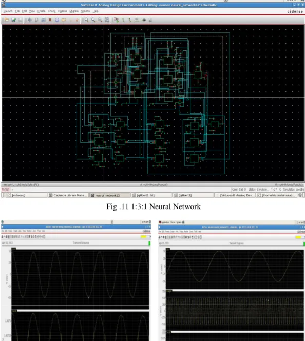
Fig .11 1:3:1 Neural Network
ximation I/O wave forms with same frequency. (b)Fu oximations (Frequency Multiplication).
he neural network with an input frequency of 500 KH etwork produced the learned 10MHz frequency as th the figure 12(b), with input, target and output frequency multiplication operation of neural network
uly 2011
104 Function
International Journal of Artific
5. Analog Operations
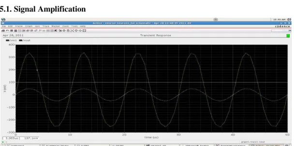
5.1. Signal Amplification
Fig.13: Tr
The linearity property of NAF(Fi can be observed that the amplitu produced output swing is of 580 input. The gain of neuron amplif small signal amplification purpos
5.2.Amplitude Modulation
Fig 14: T
One of the other applications of important building block of neur figure.14 shows its transient resp discussions the analog operation
ficial Intelligence & Applications (IJAIA), Vol.2, No.3, Jul
Transient Response of signal amplification
(Fig.6) can be used for the signal amplification, from itude of input signal is ±50mV with a frequency of 50
80mV with maintaining the constant frequency sam lifier is “5.8”. From thiswe conclude that neuron can
ose.
: Transient Response of AM modulation
of neuron is Amplitude Modulation, as analog multi uron, so its property can be used for amplitude modu esponse and modulation index obtained is “2.5”.From
n of Neural Network can be validated.
uly 2011
105 figure.13, it 500KHz, and me as that of an be used for
International Journal of Artific
6. Digital Operations
Neural architecture is also adopte These operations are obtained by voltage, and input terminals of N digital operations and its test be and NOT gates are shown in figu
Fig.
Fig
ficial Intelligence & Applications (IJAIA), Vol.2, No.3, Jul
pted and verified for Digital operations like OR, AND by varying three main properties of neuron; they are “w NAF”. The digital buffer is used at the output stage of bench is shown in figure.15. The simulated results of gure.16.
.15 Test bench for digital operation
Fig 16(a): OR gate I/O waveforms
uly 2011
International Journal of Artific
Fig
6. Applications of Neura
Artificial neural networks are of state explicit rules. Often it see examples; if sufficient data is ava
Clustering:
A clustering algorithm explores cluster. Best known applications
Classification/Pattern recogniti
The task of pattern recognition is one of many classes. This categ memory.
Function approximation:
The tasks of function approx to noise. Various engineering and
ficial Intelligence & Applications (IJAIA), Vol.2, No.3, Jul
ig 16(b): AND gate I/O waveforms
Fig 16(c): NOT gate I/O waveforms
ral Network
often used for applications in recent days, where it is seems easier to describe a problem and its solution
vailable a neural network can be trained.
es the similarity between patterns and places similar p s include data compression and data mining.
ition:
is to assign an input pattern (like handwritten sy egory includes algorithmic implementations such as
oximation are to find an estimate of the unknown func nd scientific disciplines require function approximatio
uly 2011
107 is difficult to
on by giving
r patterns in a
symbol) to as associative
International Journal of Artificial Intelligence & Applications (IJAIA), Vol.2, No.3, July 2011
108 Prediction Systems:
The task is to forecast some future values of a time-sequenced data. Prediction has a significant impact on decision support systems. Prediction differs from function approximation by considering time factor. System may be dynamic and may produce different results for the same input data based on system state (time).
Brain modeling:
The scientific goal of building models of how real brains work. This can potentially help us understand the nature of human intelligence, formulate better teaching strategies, or better remedial actions for brain damaged patients.
Artificial System Building:
The engineering goal of building efficient systems for real world applications. This may make machines more powerful, relieve humans of tedious tasks, and may even improve upon human performance.
7. Future work
The conventional computers are good for fast arithmetic and do what programmer programs, ask them to do. The conventional computers are not so good for interacting with noisy data or data from the environment, massive parallelism, fault tolerance, and adapting to circumstances.
Signal compression can be done in analog domain using neural networks, the main difference between analog and digital signal processing is, analog signal processing does not require analog to digital converter, where as digital signal processing require analog to digital and digital to analog converter. The problem of quantization noise can be avoided by analog signal processing with the help of neural network.
8. Conclusion
A VLSI implementation of a neural network has been demonstrated in this paper. Analog weights are used to provide stable weight storage with refresh circuit. Analog multipliers are used as synapse of neural networks. Although the functions learned were analog, the network is adoptable to accept digital inputs and provide digital outputs for learning other functions. Network designed has been successfully adopted for digital operations like AND, OR and NOT.
The Network proposed has following features.
Gilbert cell multiplier was designed with maximum input range of 100mV and maximum output swing of 800mV.
Neuron Activation function was designed for input range of ±1.8V and output range of ±1.7V. A Neural architecture was proposed using these components.
The Neural Architecture works on the supply voltage ±1.8V with the output swing of ±1.6V.
Back Propagation algorithm was used for the training of the network.
The designed neural architecture had a convergence time of 200 ns.
The Neural network shown to be useful for digital and analog operations.
The architecture proposed can be used with other existing architecture for neural processing.
International Journal of Artificial Intelligence & Applications (IJAIA), Vol.2, No.3, July 2011
109
R
EFERENCES[1].Gilbert Multiplier by Ari Sharon, aris@cs, Ariel Zentner , relz@cs, Zachi Sharvit, zachi@cs, Yaakov Goldberg, yaakov@cs.
[2].Bose N. K., Liang P., “Neural Network Fundamentals with graphs, algorithms and Application”, Tata McGraw hill, New Delhi, 2002, ISBN 0-07-463529-8
[3]. Razavi Behzad, “Design of Analog CMOS Integrated Circuits”, Tata McGrawhill, New Delhi,2002, ISBN 0-07-052903-5
[4]. Bernabe Linares-Barranco et al., “A Modular T-Mode Design Approach for Analog NeuralNetwork Hardware Implementations”, IEEE Journal of Solid-state Circuits. Vol. 27, no. 5, May1992, pp. 701-713
[5]. Hussein CHIBLE, “Analysis And Design Of Analog Microelectronic Neural Network Architectures With On-Chip Supervised Learning” Ph.D. Thesis in Microelectronics, University of Genoa, 1997 Isik Aybay et al, “Classification of Neural Network Hardware”, Neural Network World, IDG Co.,Vol 6 No 1, 1996, pp. 11-29
[6]. Vincent F. Koosh “Analog Computation and Learning in VLSI” PhD thesis California institute of technology, Pasadena, California.2001
[7].Roy Ludvig Sigvartsen, “An Analog Neural Network with On-Chip Learning” Thesis Department of informatics, University of Oslo, 1994 Chun Lu, Bing-xue Shi and Lu Chen, “Hardware Implementation of an Analog Accumulator for On-chip BP Learning Neural Networks” Institute of Microelectronics, Tsinghua University Beijing, China 2002
[8].Arne Heittmann, “An Analog VLSI Pulsed Neural Network for Image Segmentation using, Adaptive Connection Weights” Dresden University of Technology, Department of Electrical [9].European Journal of Scientific Research ISSN 1450-216X Vol.27 No.2 (2009), pp.199-216 [10].Engineering and Information Technology, Dresden, Germany, 2000 Shai, Cai-Qin. Geiger, Randy