Vol. 8 No 2, 02026(5pp) (2016)
Том
8
№
2, 02026(5cc) (2016)
Spray Deposited Nanocrystalline ZnO Transparent Electrodes: Role of Precursor Solvent
C.M. Mahajan
1,2,*, M. Pendharkar
1, Y.A. Chaudhari
3, S.S. Sawant
1, B. Ankamwar
4, M.G. Takwale
21
Department of Engineering Sciences and Humanities, Vishwakarma Institute of Technology, Pune
–
411 037, India
2School of Energy Studies, Savitribai Phule Pune University
–
411 007, India
3
Department of Physics, Shri Pancham Khemaraj Mahavidyalaya, Sawantwadi
–
416 510, India
4Department of Chemistry, Savitribai Phule Pune University, Ganeshkind, Pune
–
411007, Maharashtra, India
(Received 21 March 2016; revised manuscript received 10 June 2016; published online 21 June 2016)
Nanocrystalline ZnO thin films were deposited by intermittent spray pyrolysis using different alcoholic and aqua-alcoholic precursor solvents. The XRD analysis reveals the polycrystallinity of hexagonal wurtz-ite type ZnO films with preferred c-axis orientation along [002] direction. The polycrystallinity increased due to use of aqua-alcoholic precursor solvent. The crystallite size was found to vary from 41.7 nm to 59.4 nm and blue shift in band-gap energy (3.225 eV to 3.255 eV) was observed due to aqua-alcoholic to al-coholic precursor solvent transition. The films deposited using alal-coholic precursor solvent exhibited high transmittance ( 92 %) with low dark resistivity (10– 3Ωcm) as compared to aqua-alcoholic precursor sol-vent. The effect of precursor solvent on resistivity, carrier concentration ( – /cm3), carrier mobility ( – cm2V– 1s– 1), sheet resistance (Ω/ ) and figure of merit (ΦTC) is also reported. We recommend ethanol or methanol as a superior precursor solvent over aqua-alcoholic precursor solvent for deposition of device quality ZnO thin films.
Keywords: ZnO thin films, Intermittent spray pyrolysis, XRD, Electrical properties, Optical properties.
DOI: 10.21272/jnep.8(2).02026 PACS numbers: 73.61.Ga, 81.15.Rs, 61.05.C, 73.61.r, 78.66.w
*
[email protected]
1.
INTRODUCTION
Zinc Oxide (ZnO) is one of the most promising II-VI
semiconducting materials for optoelectronic
applica-tions. It is
n
type, non toxic direct wide band gap
mate-rial (
Eg
3.3 eV at 300 K) with good electrical
conduc-tivity, high excitonic binding energy (60 meV) and high
optical transmittance ( 90 %) in the visible range of
electromagnetic spectrum. Moreover, it is favourable
material for space applications because of its high
sta-bility when exposed to hydrogen plasma, high energy
radiation and chemical etching [1-4]. ZnO is abundant
and has simple crystal growth technology which makes
it favoured candidate for low cost applications such as
transparent conducting oxide (TCO), solar cells, energy
harvesters, antireflection coatings, liquid crystal
dis-plays [1-9]. Furthermore, ZnO thin films also find use
in gas sensors, ultraviolet sensors and optoelectronics
such as: blue/UV light emitting devices, laser,
photo-detectors, transparent thin-film transistors, field
emit-ters, field effect transistors [10-20].
Extensive research and development efforts on ZnO
thin film growth have been underway and device
quali-ty films have been deposited successfully by a variequali-ty
of deposition techniques. These include Chemical
Spray Pyrolysis (CSP) [3-8], Metal Organic Chemical
Vapor Deposition (MOCVD) [21], Sol-Gel [22],
Sputter-ing [23], Pulsed Laser Deposition (PLD) [24], and
Mo-lecular Beam Epitaxy (MBE) [25]. Amongst all these
techniques Sputtering, MOCVD, MBE, and PLD are
the foremost that have been able to produce device
quality films; however, they are expensive, complicated
and very hard to be commercialized. On the contrary;
the chemical spray pyrolysis (CSP) technique has
ac-quired a considerable attention because it is simple,
inexpensive, easy to commercialize and further capable
of having large area depositions [3-8]. One of the
im-portant and crucial CSP process parameter is
precur-sor solvent which decides the structural, optical and
electrical properties of the deposited films. The present
work reports the role of precursor solvent on structural
and optoelectronic properties of ZnO thin films.
2.
EXPERIMENTAL
2.1
ZnO Film Synthesis
ZnO films were synthesized by spray pyrolysis of
0.3 M, 50 ml solution of zinc acetate dihydrate
[(Zn(CH
3COO)
2.2H
2O), Merck, 99.99 % pure] on soda
lime glass substrates at deposition temperature of
450 C. In CSP technique, during film deposition, the
precursor solvent should facilitate quick
transfor-mation of precursor mist into vapor; hence due to their
high volatility ethanol / methanol are favored
precur-sor solvents. In order to investigate the proper solvent
for zinc acetate precursor to deposit ZnO thin films
with good structural and optoelectronic properties
al-coholic and aqua-alal-coholic solvents such as (a) ethanol,
(b) methanol, (c) ethanol + water (4 : 1) and (d)
metha-nol + water (4 : 1) were used to deposit thin films of
ZnO. Double distilled water was used for aqua
alcoho-lic solvents. The water is the best oxidizing agent,
however, it was not used as a solvent because under
isothermal conditions ( 130 C) water of
crystalliza-tion from zinc acetate dihydrate is evaporated (H
2O
vapors) into atmosphere causing complete oxidation
and results in clean ‘c’ axis oriented thin films of ZnO
are shown below [3, 7]:
䊺 (gas) 3
substrate) on (film e
coalescenc and n neucleatio
2 substrate) (adsorbed/ 6 3 4 adsorption
2 substrate) near (gas 2 3 heat
2 3
COOH 6CH + ZnO
4
䊻
O 3H + COO)
O(CH Zn
䊻
O H + COO)
4Zn(CH
䊻
COO)
Zn(CH (solidnear substrate)
Soda lime glass substrates were chemically and
ul-trasonically cleaned before deposition and then rinsed
in de-ionized water. The precursor solution was
inter-mittently sprayed at 2.5 ml/min flow rate (in spraying
cycles of 30 s followed by a break of 30 s to keep steady
substrate temperature) onto the hot substrate held at a
distance of 30 cm from the spray nozzle. Ultra filtered
compressed air (air flow rate
–
15 l min
– 1, air pressure
at nozzle
–
8 kg/cm
2) was used as a carrier gas. The
temperature of substrate heater (3 kW; Make: Baker
UK) was maintained constant using an electronic
tem-perature controller unit. Properly insulated housing
was used around the substrate to ensure that the
dep-osition temperature remained constant during film
synthesis. After deposition the films were annealed at
deposition temperature for 10 min for re-crystallization
effects to take place.
2.2
Characterization
The X-ray diffraction (XRD) analysis was done for
ZnO thin films by using CuK
αradiation (
1.5405
Å
)
to investigate the crystal structure and film
orienta-tion. The spectral transmittance and absorbance was
obtained using UV-VIS-NIR spectrometer (model UV-
1650 - PC) in the wavelength of 350 nm to 1100 nm.
Hall measurements were performed at room
tempera-ture and atmospheric pressure to measure electrical
properties of the film with an assumption that the
elec-trical conduction throughout the depth of the film is
homogenous. The sheet resistance was measured from
the knowledge of resistivity and thickness. The optical
transmittance and conductivity of the ZnO thin films
are the characteristics to be optimized for its use as a
transparent electrode. The dependence of carrier
con-centration (
–
/cm
3) and mobility (
–
cm
– 2V
– 1s
– 1) on
precursor solvent is discussed along with variation in
sheet resistance (
Rs
–
Ω/□) and figure of merit (Φ
TC–
Ω
– 1) for ZnO films in view of their possible
applica-tions as transparent conducting coatings and window
layers in photovoltaic and optoelectronic devices.
3.
RESULTS AND DISCUSSIONS
3.1
Structural Properties
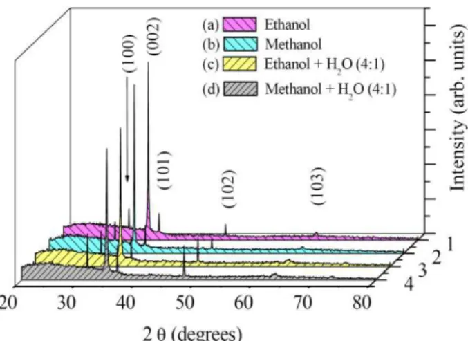
Fig. 1 shows a low angle XRD of CSP deposited ZnO
films with precursor dissolved in different solvents in
the range of 20-80 with slow scanning speed (2/min)
and step width of 0.02). As seen from the XRD, all
films are polycrystalline in nature having hexagonal
wurtzite structure with most preferred orientation
along
c
- axis [002] direction according to ASTM
stand-ards [27]. Other orientations along (100), (101), (102)
and (103) crystal planes were also observed; however,
their intensities were very weak as compared to the
[002] peak. The films deposited from ethanol and
sub-sequently methanol based precursor were most
prefer-ably oriented along [002] direction exhibiting higher
crystallinity when compared with those deposited
us-ing aqua alcoholic solvent for precursor. This may be
due to the nucleation process during film formation, if
the nucleation is preferred in the initial stage of
depo-sition, a strict improvement in preferred growth is
ob-served [28-30]. Also, the intensity for other
orienta-tions was found to be increased when alcoholic solvent
was substituted by aqua alcoholic solvent. The high
vapor pressure and low surface tension of alcoholic
solvent like ethanol or methanol enables the formation
of fine droplets during the deposition which favors the
crystalline growth of ZnO towards [002] direction. The
oxygen necessary for ZnO formation is utilized from
the evaporated water vapors from zinc acetate
dihy-drate or from the surrounding air. Alcohol also acts as
a reducing agent, which in turn controls the oxygen
deficiency, attributing to the improvement in
crystal-linity thereby lowering the crystal defect density. The
intensity values of XRD peaks for different (
h
,
k
,
l
)
planes and measured grain size
d[002]
of ZnO films
de-posited using different precursor solvents are listed in
Table 1. The classical Scherrer formula [31] as shown
in equation (1) was used to estimate the average
crys-tallite size (
D
) of crystallites / grains for the ZnO films;
cos
k
D
(1)
where the constant
k
is the shape factor usually equal
to 1,
is the wavelength of X-ray,
is the Bragg’s a
n-gle and
is the full width of the half maxima (FWHM).
Usually the widening of XRD peak is caused by
inter-nal stress and defects, so the mean grain size
estimat-ed by this method is normally smaller than the actual
value.
Fig. 1 – XRD patterns of ZnO films deposited by CSP tech-nique using different precursor solvents
3.2
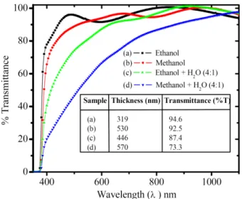
Optical Transmission and Absorption
S
PRAYD
EPOSITEDN
ANOCRYSTALLINEZ
NO…J.
N
ANO-
E
LECTRON.
P
HYS.
8, 02026 (2016)
transmittance (73 to 94 %) in the spectral range of
400 nm to 1100 nm. It can also be observed that the
optical transmittance for ZnO films obtained using zinc
acetate precursor dissolved in alcoholic solvent is
max-imum. The substantial decrease in transmittance for
ZnO films deposited using precursor dissolved in aqua
alcoholic solvent is due to poor crystallinity of these
films. The superior crystalline structure of ZnO film
due to alcoholic solvent is also established through
XRD analysis. The films thickness increases due to the
use of aqua alcoholic solvent for precursor.
Fig. 2– Spectral dependence of transmittance for ZnO films synthesized using different precursor solvents. The inset table shows variation of film thickness and transmittance (400 nm-1100 nm)
Fig. 3– Spectral dependence of absorptance for ZnO films synthesized using different precursor solvents. The inset is plot of (hν)2 vs. hν of ZnO films
Fig. 3 illustrates the variance of absorption in the
range of 350 nm to 1100 nm. It is evident that the
ab-sorption coefficient decreases with an increase in
wave-length, and a sharp decrease in absorption coefficient,
near the band edge for films deposited using precursor
dissolved in alcoholic solvent, indicates better
crystal-linity of the films and lower defect density. The
analy-sis of the transmittance and absorption spectra in the
vicinity of the fundamental absorption edge shows that
the variation of the absorption coefficient is in
accord-ance with the following relation which implies the
di-rect transitions [5].
(
h
)
h
g
(2)
The inset graph in Fig. 3 shows the variation of
(
h
ν
2) vs.
h
ν. The bandgap of the material from graph
is x-axis intercept obtained by extrapolating the linear
portion of the exponential curve. The energy gap for all
the films was found in between 3.225 to 3.255 eV.Table
1 shows the values of crystallite size (
d[002]
) and the
band gap energy for ZnO thin films deposited using
precursor dissolved in different solvents. The grain size
d
[002]was observed to be increased when alcoholic
sol-vent was replaced by aqua alcoholic solsol-vent. The
varia-tion in energy band gap with crystallite size as seen
from Table 1, clearly shows the quantum size effect of
decrease in band gap energy due to increase in
crystal-lite size.
Table 1 – Intensity data for different (h, k, l) planes, grain size (d[002]) and energy band gap (Eg) of ZnO film deposited using different precursor solvents
The film thickness was determined via the method
developed by Manifacier using the following relation [32].
1 2
1 2 2 1
2
f ft
n
n
(3)
where
nf
1and
nf
2are the refractive indices of the film
at two adjacent interference maxima or (minima) at
wavelengths
1and
2respectively (usually in this
re-gion,
nf
is nearly constant:
nf
~
nf
1~
nf
2).
3.3
Optoelectronic Properties
3.3a Electrical properties
The Hall Effect (Van der Pauw geometry) electrical
measurement technique was used to detect the charge
carrier type, carrier concentration, carrier mobility and
dark resistivity of the ZnO films. The measurements
revealed that all ZnO films were
n
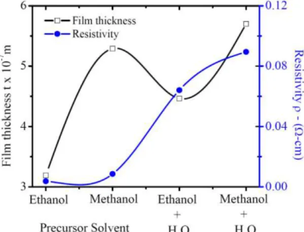
-type. The variation
in film thickness and resistivity of ZnO films deposited
using different precursor solvents is shown in Fig. 4.
The lowest resistivity (3.74 10
– 3Ω
cm) was
meas-ured for the ZnO film deposited using precursor
dis-solved in ethanol. This lowest resistivity attributes to
good crystallinity and modification of properties of the
grain boundaries which results in lower defect density.
It can be observed that the resistivity increases when
alcoholic solvent is replaced by aqua alcoholic solvent.
Precursor Solvent
I[002] I(100) I(101) I(102) Grain Size d[002] –
nm Eg
– eV
Ethanol (Eth.) Methanol (Mth.) Eth.+H2O (4 : 1) Mth.+H2O (4 : 1)
5128 4870 3994 3786
905 961 1033 1323
765 797 881 999
460 421 828 987
41.7 54.8 49.3 59.4
The grain boundary effects such as chemisorption of
oxygen (O
2–) molecular ions, poor crystallinity and
in-corporation of residual nonvolatile organic compounds
caused by incomplete decomposition of the metal
or-ganic source (zinc acetate) leads to development of
po-tential barriers at grain boundaries and on surface
which hamper the electrical transport. However,
de-sorption
of
chemisorbed
oxygen
at
deposition
Ts
400 C contributes to an excess electron in the
ZnO lattice (O
2– O
2+
e
–); hence electrical
conductivi-ty increases [33, 34]. Moreover, the closed outer 2
p
shells of O
2–ions and empty 4
s
levels of Zn
2+ions in the
crystal lattice instigate the neutralization of Zn; which
at higher
Ts
can easily ionize one electron in conduction
band increasing the conductivity [35]. The measured
resistivity value of 3.74 10
– 3Ω
cm is in good
agree-ment with those reported in the literature for ZnO thin
films [3-7].
Fig. 4 – Plot shows variation of film thickness (t), resistivity () of ZnO films synthesized using different precursor solvents
Fig. 5 – Plot shows variation of mobility (), conductivity () and carrier concentration () in ZnO films synthesized using different precursor solvents
The variation observed in electrical resistivity (
–
Ω
– 1cm
– 1), mobility of charge carriers (
–
cm
– 2V
– 1s
– 1)
and carrier concentration (
–
/cm
3) for ZnO films
depos-ited using precursor dissolved in different solvents is
shown in Fig. 5. Both carrier concentration and mobility
have higher values for alcoholic solvent based ZnO films,
whereas, the carrier concentration and mobility decrease
substantially when alcoholic solvent is replaced by aqua
alcoholic solvent. The highest values of conductivity
(268
Ω
– 1cm
– 1), carrier concentration (1.49 10
20/cm
3)
and carrier mobility (11.3 cm
2V
– 1s
– 1) were measured
for ZnO film deposited using ethanol as a precursor
solvent. Thus, disorder generated in the lattice seem to
be the main cause for the decrease in carrier
concen-tration.
3.3b Figure of Merit
This investigation shows that visible transmittance
and electrical resistivity depend significantly on
pre-cursor solvent. As already mentioned the purpose is to
use ZnO layer as transparent electrode with highest
transparency and lowest resistivity. Evaluation of the
deposited thin film, as TCO is necessary because under
optimum deposition conditions visible transmittance
and electrical resistivity depend significantly on film
thickness. The electrical resistivity decreases with
in-creasing film thickness however adversely affects its
transparency. The figure of merit predicts TCO
proper-ties by minimizing the trade-off between electrical
re-sistivity and transparency. Excellent quality TCO film
is associated with maximum value of figure of merit.
The figure of merit of the films was calculated using
the relation proposed by Haacke [36],
10
TC S
T
R
(6),
where
T
is the transmittance,
Rs
the sheet resistance.
Fig. 6 – Plot shows variation of transmittance (% T), sheet resistance (Rs) and figure of merit (ФTC) of ZnO films synthe-sized using different precursor solvents
The variation of sheet resistance (
Rs
–
Ohms/Sq.)
and figure of merit (
Ф
TC) with variation in precursor
solvent is shown in Fig. 6. It can be seen that the figure
of merit is more for ZnO films obtained by spray
pyrol-ysis of precursor dissolved in alcoholic solvent than
that of aqua alcoholic solvent. The highest figure of
merit, 4.9 10
– 3Ω
– 1, was obtained for a ZnO film
deposited using precursor dissolved in ethanol. The
corresponding value of sheet resistance is minimum
117
Ω
/
along with maximum transmittance of 94.6 %.
4.
CONCLUSIONS
S
PRAYD
EPOSITEDN
ANOCRYSTALLINEZ
NO…J.
N
ANO-
E
LECTRON.
P
HYS.
8, 02026 (2016)
technique using alcoholic and aqua alcoholic solutions
of zinc acetate on soda lime glass substrate. The XRD
analysis confirmed the polycrystalline nature of films
with preferred orientation along [002] plane. The
alco-holic precursors lead to synthesis of highly transparent
( 92 %) films with low resistivity (10
– 3Ω
cm). The
aqua-alcoholic to alcoholic precursor solvent transition
decreases the crystallite size from 59.4 nm to 41.7 nm
and results in blue shift in band-gap energy (3.225 eV
to 3.255 eV). We recommend ethanol or methanol as a
precursor solvent over aqua-alcoholic precursor
sol-vents for deposition of device quality transparent
con-ducting thin films of ZnO.
ACKNOWLEDGEMENTS
This work was financially supported by Board for
College and University Development (BCUD),
Savit-ribai Phule University of Pune, Pune, Maharashtra.
REFERENCES
1. D.C. Look, Mater. Sci. Eng. B: Solid-State Mater. Adv. Technol. 80, 383 (2001).
2. S.O. Kucheyev, J.S. Williams, C. Jagadish, J. Zou, C. Evans, A.J. Nelson, A.V. Hamza, Phys. Rev. B 67, 094115 (2003).
3. F. Paraguay D., W. Estrada L., D.R. Acosta N., E. An-drade, M. Miki-Yoshida, Thin Solid Films 350, 192 (1999). 4. D.J. Goyal, C. Agashe, M.G. Takwale, B.R. Marathe,
V.G. Bhide, J. Mater. Sci. 27, 4705 (1992).
5. A. Ashour, M.A. Kaid, N.Z. El-Sayed, A.A. Ibrahim, Appl. Surf. Sci. 252, 7844 (2006).
6. C.M. Mahajan, M.G. Takwale, Curr. Appl. Phys. 13, 2109 (2013).
7. C.M. Mahajan, M.G. Takwale, J. Alloy. Compd. 584, 128 (2014).
8. M.T. Mohammad, A.A. Hashim, M.H. Al-Maamory, Mater. Chem. Phys. 99, 382 (2006).
9. G.A. Zhu, R.S. Yang, S.H. Wang, Z.L. Wang, Nano Lett. 10, 3151 (2010).
10.M. Law, L.E. Greene, J.C. Johnson, R. Saykally, P. Yang, Nat. Mater. 4, 455 (2005).
11.V.R. Shinde, T.P. Gujar, C.D. Lokhande, Sensor. Actuat. B 120, 551 (2007).
12.G. Hua, Y. Zhang, J. Zhang, X. Cao, W. Xu, L. Zhang, Mater. Lett. 62, 4109 (2008).
13.Z.W. Pan, Z.R. Dai, Z.L. Wang, Science 291, 1947 (2001). 14.B.Y. Oh, M.C. Jeong, T.H. Moon, W. Lee, J.M. Myoung,
J.Y. Hwang, D.S. Seo, J. Appl. Phys.99, 124505 (2006). 15.L. Luo, Y.F. Zhang, S.S. Mao, L.W. Lin, Sensor. Actuat.
A-Phys. 127, 201 (2006).
16.R.S. Aga, D. Jowhar, A. Ueda, Z. Pan, W. E. Collins, R. Mu, K.D. Singer, J. Shen, Appl. Phys. Lett. 91, 232108 (2007).
17.Y.B. Li, F. Della Valle, M. Simonnet, I. Yamada, J.J. Delaunay, Nanotechnology 20, 045501 (2009). 18.W. Wu, S. Bai, N. Cui, F. Ma, Z. Wei, Y. Qin, E. Xie, Sci.
Adv. Mater. 2, 402 (2010).
19. J.H. Ahn, H.S. Kim, K.J. Lee, S. Jeon, S.J. Kang, Y.G. Sun, R.G. Nuzzo, J.A. Rogers, Science 314, 1754 (2006).
20.A. Javey, S. Nam, R.S. Friedman, H. Yan, C.M. Lieber, Nano Lett. 7, 773 (2007).
21.W. Lee, M.C. Jeong, J.M. Myoung, Acta Mater. 52, 3949 (2004).
22.J.H. Lee, K.H. Ko, B.O. Park, J. Crystal Growth 247, 119 (2003).
23.E. Fortunato, V. Assunção, A.Gonçalves, A. Marques, H. Águas, L. Pereira, I. Ferreira, R. Martins, Thin Solid Films 451-452, 443 (2004).
24.D. Valerini, A.P. Caricato, M. Lomascolo, F. Romano, A. Taurino, T. Tunno, M. Martino, Appl. Phys. A 93, 729 (2008).
25.K. Ogata,T. Komuro, K. Hama, K. Koike, S. Sasa, M. Inoue, M. Yano, Phys. Status Solidi B 241, 616 (2004). 26.A. Djelloul, K. Bouzid, F. Guerrab, Turk. Jour. Phys. 32,
49 (2008).
27.Powder Diffraction File, Data Card 5-644, 3c PDS Inter-national Centre for Diffraction Data, Swarthmore, PA. 28.C.M. Mahajan, A.G. Godbole, S.P. Gumfekar,
S.H. Sonawane, M.G. Takwale, Adv. Mater. Res. 67, 103 (2009).
29.C.M. Mahajan, M.G. Takwale, International Workshop on Physics of Semiconductor Devices, 911 (2007).
30.B. Elidrissi, M. Addou, M. Regragui, C. Monty, A. Bougrine, A. Kachouane, Thin Solid Films 379, 23 (2000).
31.H.P. Klung, L.E. Alexander, X-ray Diffraction Procedures For Polycrystalline and Amorphous Materials, 2nd Edi-tion (Wiley: New York: 1974).
32.J.C. Manifacier, Thin Solid Films 90, 297 (1982). 33.Shih-Chia Chang, J. Vac. Sci. Technol. 17 No 1, 366
(1980).
34.Y. Fujita, T. Kwan, J. Res. Inst. Catal. 7, 24 (1959). 35.L.V. Azaroff, J.J. Brophy, Electronic process in materials
(McGraw-Hill: New York: 1963).