A New Design Technique of Reversible BCD Adder Based on NMOS with Pass Transistor Gates
Texto
Imagem
Documentos relacionados
There are three major design goals in reversible logic. 1) The quantum cost, which is the number of 1*1 and 2*2 reversible calculations necessary to generate the
In this paper, we design a novel algorithm based on the strategy improvement technique, suitable for practical solving of the lower-bound and the lower-weak-upper-bound problems
The proposed Full adder can be implemented using combination of all optical reversible NOR logic gate and using all optical reversible NAND gate (NAND logic based
In this paper we have demonstrated a technique based on a 1-m scanning monochromator for ground based measurement of daytime sodium airglow emissions at 5896 ˚ A and compared it
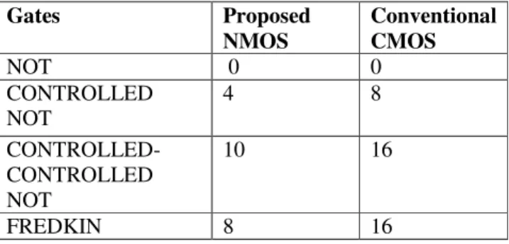
This fully differential implementation requires only 20 transistors which mean that the proposed design involves 28.57% saving in transistor count compared to
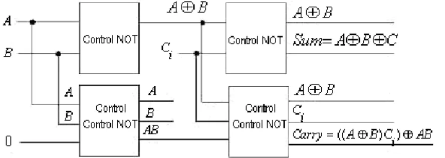
The new logic structure presented in Fig.2.Fig.6 presents a full adder designed using SR-CPL logic to obtain xor/xnor gates, pass transistor based multiplexer to get So and Co
For Full adder which having the same input counts designed with differential logic styles, the BCDL gates has larger energy as compared with domino CMOS and DCVS
In this paper, useful design hints for designing oscillator circuits based on NOT gates are supported by analyzing the response of the RO in the time domain; ROs have been designed
