Design and Analysis of Shift Register using
Pulsed Latches with Reduced Power and Area
Ch.Jyothsna Department of ECE
Narayana Engineering College, Nellore
M.Swarna Lakshmi
Assistant Professor, Department of ECE Narayana Engineering College, Nellore
M.Muralidhar Professor, Department of ECE Narayana Engineering College, Nellore
Abstract -Power consumption and Area reduction plays a major role in sequential circuit design. A novel design and analysis of a shift register using pulsed latches with reduced power and area is proposed. To reduce the area the traditional data flip-flops are substituted with pulsed latches. The use of various non overlap delay pulsed clock signals substituted by the traditional single pulsed clock signals by this design solves the timing issues in pulsed latches. In the standard system, shift register uses single pulsed clock signal for data transition, which consumes additional power. The shift register uses a small number of the pulsed clock signals and combine the latches to many sub shifter registers and exploitation further temporary storage latches. To minimize power consumption various non overlap delayed pulsed clock signal design is proposed for data synchronization in an exceedingly multi bit shift register. The proposed system is designed by using a popular Schematic and layout capture tool with 90nm technology.
Keywords: Flip-flop, pulsed clock, pulsed latch, shift register.
I.INTRODUCTION
In digital design flip-flops and latches are basic storage elements. Flip flops are precarious timing elements in digital circuits which have a great impact on speed and power consumption [2]. In VLSI chip design reducing power has become a important consideration of an performance and area. The Shift register is a type of sequential circuit it is mainly used for storage or transfer digital data.
An M-bit shift register consists of M -data flip-flops which are connected in series form [1]. The implementation of the M-data flip-flop is less important element to regulate the capability of the total synchronous circuit than the area and power consumption as a result there is no circuit present between flip-flops within the register. To reduce the area and power consumption, the smaller flip-flop is used for the register [3]. In this flip flops the transistor are more compared to pulsed latches so that the circuit has more switching and power consumption is high.
Flip-flops are replaced by pulsed latch in several applications, because pulsed latches are smaller than flip flops. The use of multiple non overlap delay pulsed clock signals substituted by the traditional single pulsed clock signals by this design solves the timing problem in pulsed latches [4]. The shift register uses a less number of the pulsed clock signals and combine the latches to many sub shift registers and exploitation further temporary storage latches.
The rest of the paper describes the proposed shift register architecture in section II. Result measures are presented in section III. Conclusion is given in section IV.
II.PROPOSED SHIFT REGISTER
as shown in fig.1(a), this pulsed latch we taken as the pulsed clock signal can be replaced by the normal clock signal as in fig.1 (b) so as a result, the size of pulsed latch size become almost half of those of the master-slave flip-flop size as a result the area and power reduces. The pulsed latch is higher resolution for area efficient and low powerconsumption.
Fig.1: (a) Master-slave flip-flop. (b) Pulsed latch.
The proposed shift register is splits into many sub shifter register M as shown in fig. 2(a). it is to narrow the delays of pulsed clock signals. The operation of proposed shift register in this first four bit sub shifter exist of five latches and it executes shift operations with five non overlap delayed pulsed clock signals as clock_ pulse <1> up to clock _pulse <T>.In the whole sub shifter register is taken as the four bit shift register #1.The four latches stores four bit of data Q1, Q2, Q3, Q4 and finally last latch stores one bit usual data as T1 as shown in fig.2(b). This T1 gives as the input next four bit shift register #2 and in this the latches stores the data as Q5 to Q8 and final last latch has the data of T2. In this the data shifts up to shift register #M. In shift register every latch exist clock pulses in this the clock pulses are generated from the delayed pulsed clock generator as shown in fig 3. In this shift register the delayed pulsed clock generator consists of delays, AND gates. In this delay circuits has the rising and falling times in all inverters so that the AND gate generated with inverters produce sharp pulsed clock signals.
Fig. 2(a): proposed shift register using pulsed latches
Fig. 2(b): proposed shift registers wave forms
Fig.3:delayed pulsed clock generator
This design implementation the proposed shift register uses the pulsed latch is SSASPL (static differential sense amp shared pulsed latch) it is smallest pulsed latch. By using this SSASPL the design of pulsed latch used in proposed shift register. The below fig .4 shows the circuit diagram of SSASPL with transistors.
III. SIMULATION RESULTS
The proposed shift register using pulsed latches is designed with SSASPL pulsed latch .and this design is designed in 90 nanometer technology and both in pre layout .After simulation delay number of transistor and power is less compare to prevail Flip-flop this is shown in table.1.
TABLE 1: COMPARISION OF PROPOSED SHIFT REGISTER
In this standard system design the flip flop circuit diagram as shown in Fig:5 and layout in Fig:6 and waveforms in Fig:7 as shown below
Fig.5: standard flip flop
Fig.6: standard flip-flop layout
PARAMETERS FLIP FLOP PULSED LATCHES% IMPROVEMENT
Total number of transistors 16 7 43.75%
Number of transistors connected to
clock 8 1
12.5%
Area 9600 5530 57.6%
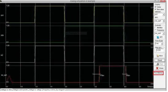
Power 0.786mW 0.184mW 23.4%
Maximum Clock frequency 2.8GHZ 483MHZ 17.25%
Fig.7: wave forms of standard flip flop
Fig.8 shows circuit of proposed shift register fig.9 shows layout of proposed shift registers and fig.10 shows wave forms of proposed shift registers.
Fig.8: proposed shift register
Fig.10: wave forms of proposed shift register
IV.CONCLUSION
The design and analysis of a shift register using pulsed latches with reduced power and area is proposed. In order to reduce the area the traditional data flip-flops are substituted placed with pulsed latches. The use of various non overlap delay pulsed clock signals substituted by the traditional single pulsed clock signals by this design solves the timing problem in pulsed latches. In the standard system, shift register uses single pulsed clock signal for data transition, which consumes additional power. The shift register uses a small number of the pulsed clock signals and combine the latches to many sub shifter registers and exploitation further temporary storage latches. To minimize power consumption multiple non overlap delayed pulsed clock signal design is proposed for data synchronization in an exceedingly multi bit shift register.
REFERENCES
[1] Byung-Do Yang “low power and area efficient shift register using pulsed latches,” IEEE Transactions on circuits and systems-1 regular papers,vol.62,no.6, pp.1564-1570,June 2015.
[2] P.Rayes,P.Ravirigo,J.A.Maestro, and O.Ruano ,“New protection techniques against SEs for moving average filters in a radiation environment,” IEEE Transactions.nuci.Sci.,vol.54,no.4 pp.957-964,aug 2007.
[3] M. Hatamian et al., “Design considerations for gigabit ethernet 1000 base-T twisted pair transceivers,” Proc.IEEE Custom Integr. Circuits Conf., pp. 335–342, 1998.
[4] H. Yamasaki and T. Shibata, “A real-time image feature-extraction and vector-generation vlsi employing arrayed-shift-register architecture,” IEEE J. Solid-State Circuits, vol. 42, no. 9, pp. 2046–2053, Sep. 2007.
[5] H.-S. Kim, J.-H. Yang, S.-H. Park, S.-T. Ryu, and G.-H.Cho, “A 10-bitcolumn-driver IC with parasitic insensitive iterative charge-sharing based capacitor-string interpolation for mobile active-matrix LCDs,” IEEE J. Solid-State Circuits, vol. 49, no. 3, pp. 766–782, Mar. 2014. [6] S. Naffziger and G. Hammond, “The implementation of the nextgeneration 64 b itanium microprocessor,” in IEEE Int. Solid-State Circuits
Conf. (ISSCC) Dig. Tech. Papers, Feb. 2002, pp. 276–504.