International Journal of VLSI design & Communication Systems (VLSICS) Vol.6, No.3, June 2015
Manali Dhar
1, Debolina Roy
2and Tamosha Saha
31
Assistant Professor, Department of Electronics & Communication Engineering,
DSCSDEC, Kolkata, India
2,3
UG Student, Department of Electronics & Communication Engineering,
DSCSDEC, Kolkata, India
A
BSTRACTIt has been almost four decades that banks and other financial organizations have been gradually computerised, in order to improve service and efficiency and to reduce cost. The birth of Electronic Fund Transfer and Automated Teller Machines has given rise to 24-hour banking and a greater variety of services for the customer. This method uses a computer to transfer debits and credits, with the help of electronic pulses, which are carried through wires either to a magnetic disk or tape. ATM (Automated Teller Machine) has become an important part in our daily lives. People use ATM for various purposes such as money withdrawal, checking balance, changing password etc. Since it mainly deals with people's money, it has to be a secure system on which we can rely. We have taken a step towards increasing this security and integrity by trying to implement the functioning of an ATM using VLSI-based programming, HDL(Hardware Description Language).The conventional coding languages such as C,C++ are replaced by VHDL(Very High Speed Integrated Circuit Hardware Description Language) so that the code cannot be easily hacked or changed. This article consists of an insight into the various functions that can be performed using an ATM, a brief description of the Coding and the obtained simulation results. It also consists of the implementation of the code using FPGA Kit (Spartan3; Model no.-XC 3S50).
K
EYWORDSATM (Automated Teller Machine), Security, HDL (Hardware Description Language), FPGA (Field Programmable Gate Array).
1. I
NTRODUCTION
In Card Authentication, the originality and validity of the card entered is checked by the system. In the Password Verification step, the user is asked to enter the preset password to access his/her bank account. This is a vital step which maintains the security of the system. If the password entered is wrong, the user is denied access to the account, otherwise access is granted. In the final step, Transaction Approval, the user is asked to enter the amount of money he/she wishes to withdraw. This amount is then checked against the balance left in the user's account. If balance is sufficient, withdrawal is approved and the transaction procedure ends. These will be discussed in further detail later in this document.
2. S
OLVING
C
ONVENTIONAL
C
ODE
I
MPLEMENTATION
U
SING
VHDL
The entire transaction process implying the various ATM functions are implemented using VHDL, as it is a more secure programming language and allows for a better design management. Also, VHDL is technology independent. The ultimate result of the coding is observed by integrating it on the Spartan FPGA Kit.
VHDL is an acronym for VHSIC Hardware Description Language (VHSIC is an acronym for Very High Speed Integrated Circuits). It is a hardware description language that can be used to model a digital system at many levels of abstraction ranging from the algorithmic level to the gate level. The digital system can also be described hierarchically. Timing can also be explicitly modelled in the same description. VHDL is a powerful language with numerous languages constructs that re capable of describing very complex behaviour.
Firstly, it allows description of the structure of a design that is how it is decomposed into sub-designs, and how those sub-designs are interconnected. Secondly, it allows the specification of the function of designs using familiar programming language forms. Thirdly, as a result, it allows a design to be simulated before being manufactured, so that designers can quickly compare alternatives and test for correctness without the delay and expense of hardware prototyping automated teller machines (ATMs) are embedded systems for financial-related services. In the development of Very Large Scale Integration technology, the Field-Programmable Gate Array (FPGA) has been widely used to implement digital systems because of its simplicity, programmability, short design cycle, fast time-to-market, low power consumption, and high density. An FPGA provides a compromise between an application-specific integrated circuit (ASIC) and a general purpose processor. Systematically design efficient, portable, and scalable register transfer level (RTL) digital circuits using the VHDL hardware description language and synthesis software. An RTL design can accommodate future simulation, verification, and testing needs, and can be easily incorporated into a larger system or reused.
2.1. VHDL CODE IMPLEMENTATION
International Journal of VLSI design & Communication Systems (VLSICS) Vol.6, No.3, June 2015
Fig.1 Flowchart of VHDL code of specified ATM functioning
In automated teller machines (ATMs) the method of electronic funds transfer is incorporated which uses a computer to transfer debits and credits with the help of electronic pulses, which are carried through wire either to a magnetic disk or tape. Using an ATM card a customer can access nearly all the facilities available from a counter service. The basic operation according to the given flowchart (Figure 1) can be explained according to the following stages. The whole process can be described as following- STAGE 1: In the first stage, the customer/card holder inserts the card at the slot provided for card insertion in the ATM machine for card authentication. If the card seems to be invalid/not inserted in a proper manner, it is indicated through the buzzer. While, if the card is valid, it automatically proceeds to the next stage. In this stage, it is verified whether the inserted card is valid or not. If it seems to be invalid, then it is indicated though the buzzer. If it is the valid one, then it further proceeds. As the next step it asks for a valid password to be inserted by the card holder. Again, if the entered password is wrong, a next chance is provided to the user to re-insert the correct password. In case of the entered password is correct at the first attempt, the system allows to proceed further. STAGE 2: In this stage, the system asks the card holder to enter a valid password. If the entered password is a wrong one, it is indicated by the buzzer. In case of a correct password, the system proceeds further.
STAGE 3: In the third stage, we have considered two options: a) Savings Account, b) Current Account.
2.2. SIMULATION TOOLS
Xilinx ISE 9.2i:
Xilinx ISE (Integrated Synthesis Environment) is a software tool produced by Xilinx company for synthesis the proposed design and analysis of Hardware Description Language(HDL) designs, enabling the developer to compile the designs, examine RTL(Register Transfer Level) diagrams, perform timing analysis(Test Bench Waveform),simulate a design's reaction and configure the target device with the programmer.
ALS-SDA-CPLD/FPGA VHDL Trainer Kit (DAUGHTER BOARD-FPGA – XILINX-XC3S50):
The ALS CPLD/FPGA TRAINER is a powerful tool that allows the user to understand the capabilities of FPGA and CPLD. Configuration is the process by which the bit streams of a design, as generated by the development software are loaded into the internal configuration memory of the FPGA or CPLD. The Spartan-3 family of Field-Programmable Gate Arrays is specifically designed to meet the needs of high volume, Cost-sensitive consumer electronic applications. Spartan-3 FPGAs are ideally suited to a wide range of consumer electronics applications; including broadband access, home & broad range networking, display/projection and digital television equipment.
Fig.2 XC-3S50 FPGA VHDL TRAINER KIT
International Journal of VLSI design & Communication Systems (VLSICS) Vol.6, No.3, June 2015
The SPARTAN-3 FPGA of XILINX uses SRAM technology. SPARTAN-3 devices support serial configurations, using the master/slave serial and JTAG modes, as well as byte-wide configuration employing the Slave Parallel mode.
Spartan-3 devices support the following four configuration modes:
• Slave Serial mode • Master Serial mode
• Slave Parallel mode ARTAN
• Boundary-scan mode
Fig.3 Connection diagram of Base-Board
2.3. SIMULATION PROCEDURE
Table1. PORT Depiction
Using the software, Xilinx 9.2i ISE the implementation of the ATM code is performed practically. The FPGA hardware used is Spartan 3 series on which we have implemented and practically performance of the ATM code is carried out successfully. The simulation results are presented in the next section with the snapshots of the hardware implementation we have carried out.
2.4. SIMULATION RESULTS
RTL Schematic Diagrams are given in Fig.4. & Fig.5, which we have obtained by simulating the VHDL code using Xilinx 9.2i software, is implemented in the software and the corresponding RTL views are obtained.
The RTL schematics are followed by the Test Bench waveform (user friendly input) in Fig.6 and its respective simulation output in Fig.7 which has been obtained by giving certain conditions to the Test Bench waveform as inputs.
International Journal of VLSI de
Fig 5.RT
Fig 6.Testb
Fig
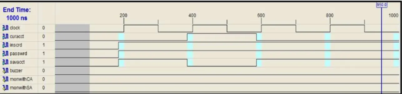
In the test bench waveform, as it The CURRACCT, INSCRD, PA made true. The simulation outpu following simulation description
design & Communication Systems (VLSICS) Vol.6, No.3,
.RTL Schematic Diagram-2 of Xilinx 9.2i ISE
stbench Waveform generated by Xilinx 9.2i ISE
ig 7. Simulation Output of Xilinx ISE 9.2i
it is visible from the figure, certain conditions are giv PASSWRD options are entered as 1 which means thes
put according to the given inputs may be explained acc on table.
.3, June 2015
Table 2. SIMULATION PORT Depiction
Condition 1:- We have considered another condition where the SAVACCT, INSCRD, PASSWRD are selected and the test bench waveforms and simulation outputs are obtained as follows-
Fig 8. Test bench Waveform generated by Xilinx 9.2i ISE
International Journal of VLSI design & Communication Systems (VLSICS) Vol.6, No.3, June 2015
This simulation output may be explained in a similar manner following the previous description table-
Table 3. SIMULATION PORT Depiction (Condition 1)
In the simulation outputs (Fig 7 & Fig 9), for both the cases certain ports are obtained as undefined (U) for a certain clock pulse. This indicates that for that particular clock pulse, the state of the ports could not be determined and hence they remain undefined.
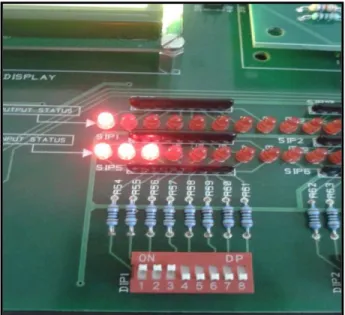
In the above figure, the output of the first condition is shown. Here the INSCRD, PASSWRD, SAVACCT options as entered as 1 through the switches DIP1-1, 2 and 3 respectively. Hence the three corresponding LEDs of the SIP5 (INPUT LED) series are turned on showing the inputs. While, the first LED of the SIP1 (OUTPUT LED) series shows that the output port or MONWITHSA port is ON as well as working according to programme.
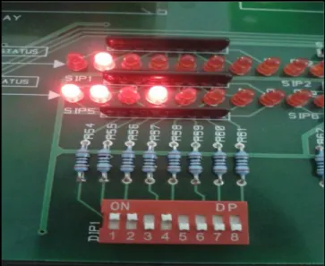
Fig 11. Simulation Output of FPGA VHDL Trainer Kit
In this figure, the INSCRD, PASSWRD AND CURRACCT options are selected through the switches 1,2 and 4 respectively which are shown through the first, second and fourth LEDs of the SIP5 series. The respective output port i.e. the MONWITHCA port is turned high and is thus shown by the second LED of the SIP1 series. Thus the FPGA implementation is accomplished successfully.
3. C
ONCLUSION
We have taken a step towards improving the security and integrity of an ATM using VHDL, keeping its original functioning intact. This is a new technology which may prove to be highly useful. This idea can gradually grow alongside the existing technologies to provide mankind with a more efficient and secure banking service. Using VHDL can reduce the menace posed by hackers, and many other such illegal activities which is a worldwide problem these days. Further, FPGA is a new and user-friendly technology which has found an important place in modern day research and development. This is flexible and can be combined with various software to yield in-vitro results. Thus, we sincerely hope that in the near future, this implementation will gain popularity and will be a significant contribution to the vast field of electronics technology.
A
CKNOWLEDGEMENTSInternational Journal of VLSI design & Communication Systems (VLSICS) Vol.6, No.3, June 2015
REFERENCES
[1] Yingxu Wang and Yanan Zhang, “The Formal Design Model of an Automatic Teller Machine (ATM)” University of Calgary, Canada, International Journal of Software Science and Computational Intelligence, 2(1), 102-131, January-March 2010.
[2] Avenet Avenue, user’s guide, Xilinx® Spartan™-3 Development Kit.
[3] Stanley MAZOR and Patricia LINGSTRAAT, "A guide to VHDL (2nd Edition)", copyright 1993, Kluwer Achedamic Publishers, pp no: 1-1 to 7-16.
[4] http://www.fpga.com.cn/hdl/training/Vhdl_Golden_Reference_Guide.pdf
[5] Peter J. Ashenden and Jim Lewis, "The Designer's Guide to VHDL (3rd Edition)" copyright 2008, Morgan KJaufmann Publication, pp no:207-225.
[6] Pong P. Chu "RTL Hardware Design Using VHDL, Coding For Efficiency, portability and Scalability", Willy Interscience a john wilay & sons, inc., Publication, pp no:23-160.
[7] Hardware Implementation of Watchdog Timer for Application in ATM Machine Using Verilog and FPGA Iqbalur Rahman Rokon, Toufiq Rahman, Md. Murtoza Ali Quader, and Mukit Alam,International Conference on Electronics, Biomedical Engineering and its Applications (ICEBEA'2012) Jan. 7-8, 2012 Dubai
AUTHORS
[1] First Author – Manali Dhar, M.Tech (Microelectronics & VLSI Design), Dr. Sudhir Chandra Sur Degree Engineering College, Assistant Professor, Dept. of ECE, JIS Group and [email protected]
[2] Second Author – Debolina Roy, Final Year B.Tech Student (Electronics & Communication Engineering), Dr. Sudhir Chandra Sur Degree Engineering College, JIS Group