Article
Printed in Brazil - ©2017 Sociedade Brasileira de Química0103 - 5053 $6.00+0.00
*e-mail: [email protected]
ITO Obtained by Spray Pyrolysis and Coating on Glass Substrate
Beatriz M. de Campos,a Gabriela S. Freiria,a Katia J. Ciuffi,a Emerson H. de Faria,a
Lucas A. Rocha,a Eduardo J. Nassar*,a and Milton S. F. de Limab
aUniversidade de Franca, Av. Dr. Armando Salles de Oliveira, 201, CP 82, 14404-600 Franca-SP, Brazil
bInstituto de Estudos Avançados (IEAv), Rod. dos Tamoios, km 5.5, 12228-970 São José dos Campos-SP, Brazil
Conductive thin films have various applications in different technological fields. Indium tin oxide (ITO) is a mixed oxide. In the film form, ITO has been widely employed as electrode in many optoelectronic devices. Methods like thermal evaporation, sputtering, chemical vapor deposition (CVD), electron beam, spray coating, and sol-gel synthesis give ITO thin films. In this work, we prepared ITO thin films by dip coating of a glass substrate into ITO obtained by spray pyrolysis. ITO consisted of spherical particles with different diameters. The ITO thin films were treated with laser. X-ray diffraction (XRD) analysis confirmed that spray pyrolysis produced spherical ITO particles. Transmittance analyses revealed the production of transparent films with thickness ranging from 0.800 to 1.200 µm. The four-wire test showed that the porosity of the films led to low conductivity. Film resistance was a function of the number of layers of ITO thin film.
Keywords: inorganic compounds, oxides, sol-gel chemistry, X-ray diffraction
Introduction
For several decades, the sol-gel process has been known to produce high-tech materials such as glass, ceramics, semiconducting thin films, luminescent materials, composites, and organic-inorganic hybrids.1 Basically,
these materials consist of a network of oxides obtained by inorganic polymerization reactions2-4 in solution. The
sol-gel process enables control of all the process steps, affording materials in the powder,5 monolith,6 and film
forms.7 All these materials display special characteristics
and properties. In addition, the sol-gel process provides materials for application in several devices like photovoltaic cells, liquid crystal displays (LCD screens), image sensors, windscreen (smart window), touch screens, among others.8
Indium oxide doped with tin (ITO) is a semiconducting material with wide band gap. ITO is transparent in the visible region of the electromagnetic spectrum and serves as a transparent conductive oxide (TCO). ITO thin films are widely used as electrode in many optoelectronic devices that require optical transparency to visible light combined with low electrical resistance.9,10
Spray pyrolysis, an aerosol process, has been employed to synthesize various materials. The initial solution
is nebulized, causing the solvent to evaporate within a few seconds. This technique preferentially affords spherical particles in one step. Particles with spherical morphology can be easily accommodated, to produce more homogeneous coatings as compared to packaging of irregular particles.11-13
Laser constitutes an important tool in materials processing. The structure of a solid surface enables to manufacture three-dimensional materials so that it is possible to repeat the surface pattern accurately all over their surface. Surface modification can help to change the physical and chemical properties of materials.14,15 Laser
has been used for various purposes, such as the treatment of surfaces, and has proven to be an appropriate alternative strategy to other methodologies. Laser has been employed to clean surfaces16 prepared by ablation because it allows
metallic material to be precisely removed without thermally damaging the adjacent regions.17,18 Laser can also be used
to form channels (printed circuits) with different shapes, sizes, lengths, depths, and spacing for specific applications like nanoconductors and waveguides, for instance.
Preparation and cleaning of substrate
Microscope glasses were used as substrate to deposit the films. The substrates were cleaned with soap and deionized water and treated in an ultrasonic bath for 15 min. Then, they were placed in acetone and ultrasonic bath, which was followed by drying with extra soft paper without manual contact.
Preparation of aqueous solution of indium chloride
Due to the temperature of the synthesis, the spray pyrolysis system required only 10% ethanol. Therefore, indium chloride was prepared in aqueous solution, which prevented further combustion. Initially, 2.5 g of In2O3 was
dissolved in ethanol and distilled water. Before heating, HCl was added, and the pH was measured and kept constant at 2.0.
Preparation of tin chloride
A 100 mL tin chloride (Aldrich) solution was prepared in ethanol.
Preparation of a solution of indium chloride doped with tin chloride for use during spray pyrolysis
The solutions of indium chloride and tin chloride were mixed in a beaker at a 135:15 v/v ratio (0.027 and 0.003 mol, respectively) and subjected to magnetic stirring for 1 h. Then, the solution was submitted to spray pyrolysis. Ultrasonic vibrations of a piezoelectric pellet (2.4 MHz) generated the spray. The droplets were drawn into a drying area that was maintained at 100 °C and then into a decomposition/densification area that was kept at 700 °C. The powder was collected by an electrostatic filter under potential gradients of 7 kV.
Preparation of the ITO suspension
After spray pyrolysis, 0.100 g of ITO was added to 11.0 mL of tetraethylorthosilicate (TEOS), 11.3 mL of ethanol, and 1.45 mL of water. The mixture was submitted to magnetic stirring for 1 h and to ultrasonic bath for 15 min. The solution remained at approximately 15 °C for weeks.
Preparation of films
The films were prepared in duplicate. They were completely transparent to visible light; the withdrawal rate
Laser treatment
The conditions were as follows: focal distance, 286 mm; laser speed, 50 cm s-1; area, 2.15 × 2.15 cm; current, 16.9 A;
power, 11 W; pulse rate, 5 kHz (5000 pulses per second);
and cooling time, 1 min between each laser step.
The Nd:YAG laser was used to treat the surface of the films. Three treatments were conducted, namely 50, 75, and 95%. The laser pulse reached a circular area in the film denominated focal diameter. The second pulse overlapped with a percentage of the area reached by the first pulse, and so on. The percentages of 50, 75, and 95% corresponded to the treated percentage relative to the previous laser pulse.18
Characterization
X-ray diffraction (XRD) analysis of the powder samples was conducted on a Rigaku Geigerflex D/Max-C diffractometer working with monochromator CuK radiation (λ = 1.5405 Å) at room temperature. Diffractograms were
recorded in the 2θ range of 5 to 75°, at a resolution of
0.04°. Scanning electron microscopy (SEM) was performed under an electron microscope TESCAN (VEGA 3 SBH model) equipped with W filament of 30 kV, at a resolution of 3 nm; secondary electrons (SEs) and beam secondary electrons (BSEs) detectors aided the investigation of particle morphology. The molecular vibration modes were analyzed by infrared spectroscopy (IR) from 400 to 4000 cm-1,
accomplished on a PerkinElmer Frontier spectrophotometer operating in the ATR (attenuated total reflectance) mode.
The four-wire test (TQF) was carried out by direct current at room temperature. Four wires were fixed on two copper plates (such as contact) measuring 2.5 and 2.0 cm. This was done to investigate whether the films presented conductance capacity. The measurements were performed on Keithley source equipment/measure unit model 2400.
Table 1. Name, number of layers of ITO thin film, and laser treatment
of the films
Film Number of layers of
ITO thin film Laser treatment / %
B01/W 1 without treatment
B01/50 1 50
B01/75 1 75
B01/95 1 95
B02/75 2 75
B03/75 3 75
Results and Discussion
X-ray diffraction of the ITO powder
Figure 1 shows the XRD pattern of the sample powder obtained by spray pyrolysis.
The XRD diffractogram (Figure 1) did not present the typical peaks of tin oxide at 2θ = 26.6° and 51.9°
(card No. 88-287 for SnO2, Search-Match software) at
a 2:1 ratio, respectively, or at 2θ = 30.9° and 33.3° (card
No. 85-712 for SnO) at a 3:1 ratio, respectively. The XRD of the ITO powder obtained by spray pyrolysis displayed the characteristic peaks of indium and tin oxide with the formula (In1.94Sn0.06)O3, card No. 89-4596 (cubic system),
and peaks related to cards No. 21-406 and 73-1809 of In2O3
in the rhombohedral system.19-21
Scanning electron microscopy (SEM) of the ITO powder
Figures 2a and 2b contain the SEM images of the sample prepared by spray pyrolysis.
The micrographs revealed formation of spherical particles with different diameters, as described in the
literature.22,23 The voltage used during spray pyrolysis
enabled control of the spherical particle size. As expected from the voltage values used during the synthesis, the approximate sizes of the spherical beads were 100 nm, 500 nm, and 2 µm (Figure 2). Larger particles tended to break due to formation of pores during spray pyrolysis.22
Infrared (IR) spectroscopy of the ITO suspension in TEOS and of the ITO powder
The IR spectrum of the ITO suspension in the TEOS solution used to obtain the ITO thin films by dip coating displayed bands at 962, 1048 and 1114, 1402, 2900, 2967, and 3343 cm-1, typical of Si−OH stretching (due to TEOS in
the suspension),6,24,25 Si−O−Si asymmetric stretching (due
to TEOS in the suspension), Sn−OH, In−OH,21,26 C−H, and
O−H (due to water in the suspension),6,24-26 respectively.
Figure 3 illustrates the IR spectrum of ITO powder and ITO in solution.
The infrared spectrum of the ITO powder exhibited the characteristic vibration mode of In−O at 489 cm-1.27,28 The
bands at 780 and 854 cm-1 were ascribed to the different
vibration modes of In–OH.27 The infrared spectrum of ITO
in solution displayed bands at 797 and 880 cm-1 and at 965,
1049, and 1085 cm-1, ascribed to silanol groups (Si−OH)
and Si−O−Si stretching, respectively.29
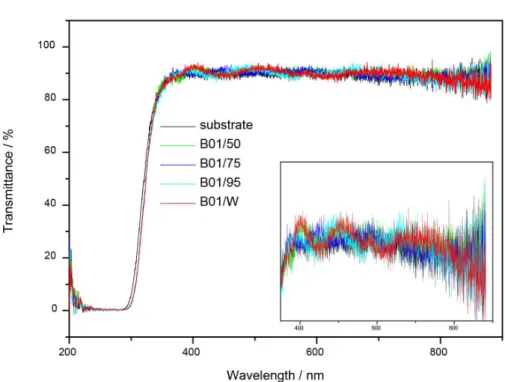
Transmittance of the ITO thin films
The optical transmittance values at 350 nm were > 90% for all the films. Considering that layers coated both sides of the substrate, the films were indeed very thin.
Figure 4 depicts the transmittance of the ITO thin films before and after treatment with laser for a series containing
Figure 1. XRD pattern of the ITO powder sample obtained by spray pyrolysis. (*) Card No. 89-4596, (o) card No. 21-406, and (x) card No. 73-1809.
Figure 3. Infrared spectra of (a) ITO in solution and (b) ITO powder.
Figure 4. Transmittance of the ITO thin films after laser treatment: substrate, B01/W, B01/50, B01/75, and B01/95.
Table 2. Film thickness and band gap of the ITO film samples containing one layer of ITO thin film
Sample B01/W B01/50 B01/75 B01/95
Thickness / µm 1.07 0.72 0.99 1.00
Band gap / eV 3.56 3.53 3.53 3.52
one layer of ITO thin film treated with 50, 75, and 95% laser treatment.
The transmittance spectra of the films helped to assess film thickness by interference fringes calculated by equation 130 (see Table 2 for the values of film thickness).
2t = N / (v1− v2) (1)
where, t is the film thickness (cm); N the number of
interference fringes; v1 and v2 are the frequency ranges
Equation 2 gives the optical band gap (Eg, also listed in Table 2) of the films obtained from the optical transmission spectra:31
Eg (eV) = 1241.5 / λc (2)
where, λc is the inflexion point of the UV absorption edge.
Film thickness was in the order of micrometers. The film without laser treatment presented the largest thickness, which showed that laser promoted particle sintering when the solvent was removed. The thickness of the films with 75 and 95% laser treatment was practically the same, but the film with 50% laser treatment had the smallest thickness. Hence, laser treatment modified the film surface, as we will discuss later in the section about SEM analysis.
The band gap for ITO films was 3.5 eV, which agreed with literature data.31,32
Table 3 summarizes the thickness and band gap values of the films containing different number of layers of ITO thin film. The values were obtained by equations 1 and 2, before and after laser treatment.
Film thickness increased by going from one to two, three, or four layers (1.07, 1.41, 1.43, and 1.40 µm, respectively). The thickness of the films containing two, three, or four layers was similar, showing that the spherical particles obtained by spray pyrolysis accommodated in the film. Laser treatment reduced film thickness in all cases because this treatment eliminated the residual solvent used to deposit the films on the glass substrate. The band gap remained practically the same regardless of the number of layers and laser treatment.
Scanning electron microscopy (SEM) of the ITO films
Figures 5-8 display the micrographs of the ITO thin films prepared by dip coating of the glass substrate into the ITO suspension obtained by spray pyrolysis without laser treatment (B01/W) and with 50% (B01/50), 75% (B01/75), and 95% (B01/95) laser treatment, respectively. The surface plot analysis performed by the open-source program ImageJ 1.49v provided the inserted images.
Table 4 lists the values of thickness obtained for the ITO film samples containing one layer of ITO thin film as calculated by equation 1 and SEM.
Considering equation 1, samples B01/75 and B01/95 had similar film thickness, which was close to one. This indicated that the films obtained after laser treatment were more homogeneous. As for samples B01/W and B01/50,
Table 3. Film thickness and band gap values obtained for the ITO film samples containing different number of layers of ITO thin film, before and after laser treatment
Sample B01/W / B01/75 B02/W / B02/75 B03/W / B03/75 B04/W / B04/75
Thickness / µm 1.07 / 0.99 1.41 / 0.94 1.43 / 0.97 1.40 / 1.02
Band gap / eV 3.56 / 3.53 3.59 / 3.57 3.60 / 3.57 3.58 / 3.55
Figure 5. Micrograph of the ITO film sample containing one layer of ITO thin film, without laser treatment (B01/W): (a) surface, (b) thickness, and (insert) surface plot analysis.
Figure 6. Micrograph of the ITO film sample containing one layer of ITO thin film, with 50% laser treatment (B01/50): (a) surface, (b) thickness, and (insert) surface plot analysis.
they had significantly different thickness because they contained particles of different sizes, which produced an irregular surface. Figure 9 evidences the irregular and rough B01/W surface; with the particles indicated in the figure.
The micrographs presented in Figures 10-12 revealed formation of continuous and homogeneous films with a thickness of approximately 1.00 µm for the samples B02/75, B03/75, and B04/75. Interaction between the nuclei was favored,33 to generate a continuous film.34
Film homogeneity attested that interdiffusion occurred between the liquid and solid interfaces, favoring rapid kinetics between the cores during the film formation.33-35
The presence of cracks in Figure 12 was due to mechanical breakdown of the film during preparation of the sample for
Figure 8. Micrograph of the ITO film sample containing one layer of ITO
thin film, with 95% laser treatment (B01/95): (a) surface, (b) thickness, and (insert) surface plot analysis.
Table 4. Values of film thickness obtained for the ITO film samples
containing one layer of ITO thin film as calculated by equation 1 and SEM
Sample B01/W B01/50 B01/75 B01/95
Thickness (equation 1) / µm 1.07 0.72 0.99 1.00
Thickness (SEM) / µm 1.50 1.70 0.80 1.00
analysis in a scanning electron microscope. The presence of cracks in the film and fracture in the glass could be attributed to force exerted by the equipment diamond pen, which broke the substrate/film.
Table 5 compares the values of thickness obtained by equation 1 and SEM for the ITO film samples containing one, two, three, or four layers of ITO thin film with 75% laser treatment.
The thickness values agreed well with the results of transmittance analysis and microscopy analysis. Film
Figure 9. SEM of the B01/W surface.
Figure 10. Micrograph of the ITO film sample containing two layers
of ITO thin film, with 75% laser treatment (B02/75): (a) surface, (b) thickness, and (insert) surface plot analysis.
Figure 11. Micrograph of the ITO film sample containing three layers
of ITO thin film, with 75% laser treatment (B03/75): (a) surface, (b) thickness, and (insert) surface plot analysis.
homogeneity depended on the number of ITO layers and on laser treatment.
Four-wire test
Four-wire test was used to measure the electric resistance. The measurements were conducted under continuous current to evaluate whether the films presented conductance capacity. The sheet resistance (Rs) can be calculated via the following relationship (equation 3):27
Rs = π/ln 2 × (V/I) (3)
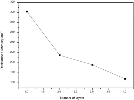
where V and I are the voltage and the current, respectively. Figures 13 and 14 show how the resistance of the ITO thin films varied as a function of the laser treatment and of the number of layers of ITO thin film, respectively.
Film resistance augmented with increasing laser filling. The high resistance was ascribed to the film porosity, which remained even after particle sintering by laser treatment. Li et al.36 also attributed porosity to the sol-gel process.
Film resistance decreased with increasing number of layers of ITO thin film. In the literature, resistance
depends on the thickness of the film from 3900 to
−17.5 kohm square-1 and from 46.9 to 3.6 kohm square-1
for ITO and ITO-PVP films, respectively.27 Decreased
resistance upon increasing thickness of the film could be due to larger ITO particle size and packing of the spherical particles obtained by spray pyrolysis in the glass substrate. According to literature papers,37,38 lower resistance of the
ITO film with increasing number of layers of ITO thin film could result from rearrangement of the layers due to temperature-dependent crystal growth.
Conclusions
Indium oxide doped with tin (ITO) can be prepared by spray pyrolysis. Dip coating then produces films from the ITO powder suspension. The resulting films are completely transparent to visible light. X-ray diffraction analysis reveal the characteristic peaks of the cubic phase of (In1.94Sn0.06)O3
and of the rhombohedral phase of In2O3. According to
electron scanning microscopy, the powder sample contains spherical ITO particles with different diameters, whereas the thin film samples consist of continuous, uniform films with thickness ranging from 800 to 1200 nm. The surface of the laser-treated films also contains particles. Film homogeneity favors interdiffusion between the liquid and solid interface. The infrared spectrum of the aliquots collected every week during aging of the ITO suspension evidence the characteristic bands of silanol groups, tin hydroxide, indium hydroxide, methyl groups, and hydroxyl groups, which are due to the presence of water and TEOS region in the suspension. Regarding electrical properties,
Table 5. Values of film thickness values obtained for the ITO film samples containing different numbers of layers of ITO thin film as calculated by equation 1 and SEM
Sample B01/75 B02/75 B03/75 B04/95
Thickness (equation 1) / µm 0.99 0.94 0.97 1.02 Thickness (SEM) / µm 0.80 0.80 1.00 1.15
the films display low current and high electrical resistance, which provide them with high insulating capacity.
Acknowledgments
The authors acknowledge CNPq and CAPES (Brazilian research funding agencies) for supporting this work. B. M. C. (grant 2012/22927-6), G. S. F. (grant 2013/22606-8), L. A. R. (grant 2011/15757-4), and E. J. N. (grant 2012/11673-3) thank the São Paulo Research Foundation (FAPESP, Brazil) for their scholarships.
References
1. Menezes, W. G.; Camargo, P. H. C.; Oliveira, M. M.; Evans, D. J.; Soares, J. F.; Zarbin, A. J. G.; J. Colloid Interface Sci.2006,
299, 291.
2. Hench, L. L.; West, J. K.; Chem. Rev.1990, 90, 33.
3. Livage, J.; Henry, M.; Sanchez, C.; Prog. Solid State Chem.
1988, 18, 259.
4. Yoldas, B. E.; J. Mater. Sci.1986, 21, 1087.
5. Matias, C. R.; Nassar, E. J.; Dexpert-Ghys, J.; Verelst, M.; Rocha, L. A.; J. Braz. Chem. Soc. 2015, 26, 2558.
6. Azevedo, C. B.; Batista, T. M.; de Faria, E. H.; Rocha, L. A.; Ciuffi, K. J.; Nassar, E. J.; J. Fluoresc. 2015, 25, 433. 7. Rocha, L. A.; Ciuffi, K. J.; Sacco, H. C.; Nassar, E. J.; Mater.
Chem. Phys. 2004, 85, 245.
8. Jimenez, L. C.; Méndez, H. A.; Páez, B. A.; Ramirez, M. E.; Rodrigues, H. B.; J. Appl. Phys.2006, 36, 1017.
9. Purica, M.; Iacomi, F.; Baban, C.; Prepelita, P.; Apetroaei, N.; Mardare, D.; Luca, D.; Thin Solid Films 2007, 515, 8674.
10. Ba, J.; Rohlfing, D. F.; Feldhoff, A.; Brezesinski, T.; Djerdj, I.; Wark, M.; Niederberger, M.; Chem. Mater.2006, 18, 2848.
11. Kang, H. S.; Kang, Y. C.; Park, H. D.; Shul, Y. G.; Mater. Lett.
2003, 57, 1288.
12. Rocha, L. A.; Freiria, J. C.; Caiut, J. M. A.; Ribeiro, S. J. L.; Messaddeq, Y.; Verelst, M.; Dexpert-Ghys, J.; Nanotechnology
2015, 26, 335604.
13. Rocha, L. A.; Caiut, J. M. A.; Messaddeq, Y.; Ribeiro, S. J. L.; Martines, M. A. U.; Freiria, J. C.; Dexpert-Ghys, J.; Verelst, M.; Nanotechnology 2010, 21, 155603.
14. Viana, R.; de Lima, M. S. F.; Sales, W. F.; da Silva, W. M.; Machado, A. R.; Surf. Coat. Technol.2015, 485.
15. Souza Neto, F.; Neves, D.; Silva, O. M. M.; Lima, M. S. F.; Abdalla, A. J.; Procedia Eng. 2015, 114, 181.
16. Verdier, M.; Costil, S.; Coddet, C.; Oltra, R.; Perret, O.; Appl. Surf. Sci.2003, 205, 3.
17. Semak, V. V.; Dahotre, N. B. In Lasers in Surface Engineering; Dahotre, N. B., ed.; ASM International: Northeast Ohio, 1998, ch. 1.
18. Arroyo, J. M.; Diniz, A. E.; de Lima, M. S. F.; Wear2010, 268, 1329.
19. Hay, J. N.; Raval, H. M.; J. Sol-Gel Sci. Technol.1998, 13, 109. 20. De, A.; Biswas, P. K.; Manara, J.; Mater. Charact.2007, 58,
629.
21. Silva, G. M.; de Faria, E. H.; Nassar, E. J.; Ciuffi, K. J.; Calefi, P. S.; Quim. Nova2012, 35, 473.
22. Freiria, G. S.; Nassar, E. J.; Dexpert-Ghys, J.; Verelst, M.; Rocha, L. A.; J. Lumin.2016, 169, 844.
23. Ferreira, C. M. A.; Freiria, G. S.; de Faria, E. H.; Rocha, L. A.; Ciuffi, K. J.; Nassar, E. J.; J. Lumin.2016, 170, 686.
24. Wang, X. D.; Shen, Z. X.; Sang, T.; Cheng, X. B.; Li, M. F.; Chen, L. Y.; Wang, Z. S.; J. Colloid Interface Sci.2010, 341, 23.
25. Nassar, E. J.; Nassor, E. C. O.; Ávila, L. R.; Pereira, P. F. S.; Cestari, A.; Luz, L. M.; Ciuffi, K. J.; Calefi, P. S.; J. Sol-Gel Sci. Technol.2007, 43, 21.
26. Wen, S. E.; Cheng, L.; Wei, J.; J. Am. Ceram. Soc.2008, 91, 1121.
27. Kőrösi, L.; Papp, S.; Dékány, I.; Thin Solid Films2011, 519, 3113.
28. Zhi-Hua, L.; Yu-Peng, K.; Dong-Yan, R.; Trans. Nonferrous Met. Soc. China2008, 18, 366.
29. Silva, G. M.; de Faria, H. E.; Nassar, E. J.; Ciuffi, K. J.; Calefi, P. S.; Quim. Nova 2012, 35, 473.
30. Cardoso, W. S.; Longo, C.; de Paoli, M. A.; Quim. Nova2005, 28, 345.
31. Bouzidi, A.; Omri, K.; Mir, L. E.; Guermazi, H.; Mater. Sci. Semicond. Process.2015, 39, 536.
32. Sarhaddi, R.; Shahtahmasebi, N.; Rokn-Abadi, M. R.; Bagheri-Mohagheghi, M. M.; Physica E2010, 43, 452.
33. Sadoh, T.; Tsunoda, I.; Nagata, T.; Kenjo, A.; Miyao, M.; Thin Solid Films 2003, 427, 96.
34. Yu, Z. D. J.; Xu, H.; Cui, Y.; Yang, Y.; Qian, G.; Thin Solid Films
2013, 544, 296.
35. Huang, Z. H.; Zeng, X. T.; Sun, X. Y.; Kang, E. T.; Fuh, J. Y. H.; Lu, L.; Thin Solid Films2009, 517, 4810.
36. Li, W.; Varlamov, S.; Huang, J.; Thin Solid Films2015, 576, 42.
37. Kim, S. S.; Choi, S. Y.; Park, C. G.; Jin, H. W.; Thin Solid Films
1999, 347, 155.
38. Liu, J.; Wu, D.; Zeng, S.; J. Mater. Process. Technol.2009, 209, 3943.
Submitted: April 13, 2017