Abstract—In this study, we have fabricated the aligned ZnO nanorods array by chemical bath deposition (CBD) on Indium Tin Oxide (ITO) glass. It can be seen that the top view of nano-structure and material compositions by scanning electron microscopy (SEM) and X-ray diffractometer (XRD). We obtained different diameter of ZnO nanorods by controlling the ZnO growth time and molar concentration of chemical solution. The results demonstrate the diameters of rod will increase by increasing the concentration. The larger ZnO nanorods arrays show a strongest diffraction peak (002) in the XRD pattern. The cyclic voltammograms (CV) and electrochemical impedance spectroscopy (EIS) were used to analyze the electrochemical characteristics of ZnO nanorods array films. The modified electrode was shown to have the best biosensing current response by coating three four seed layers.
Index Terms— ZnO nanorod; Chemical bath deposition; Modified ITO electrode
I. INTRODUCTION
inc oxide (ZnO) has attracted many attention due to its versatile properties that are quite favorable for different applications such as solar cell, gas sensor, transistor and optoelectronic devices [1-6]. Zinc oxide is a typically n-type, direct wide-band-gap Ⅱ-Ⅵ semiconductor with band gap of 3.37 eV and a large excitionic binding energy of 60 meV at room temperature [7]. The structure of ZnO plays an important role in crystal growth. It crystallizes normally in a wurtzite structure with a hexagonal lattice that has lattice constants with a length of 0.3296 nm in a-axis and 0.52065 nm in c-axis [8]. The tetrahedral structure is constructed by numerous Zn2+ and O2- ions, where Zn2+ is on the center of
tetrahedral and O2- is located in the corner of tetrahedral and
stacked along the c-axis [8]. ZnO is a polar semiconductor material with two crystallographic planes that have opposite polarity and different surface relaxation energies. The properties lead to a higher growth rate along the c-axis, where
the Zn2+ ions along the dirction (0 0 0 1) and O2- ions along
the direction (0 0 0 -1) and the nanorod-like vertical structures was formed [7].
Since the direct band gap of ZnO is 3.37 eV which is larger than the energy gap of visible light, 3.1 eV. It leads the visible light could not stimulate the electron of ZnO from valance band to conduction band. Thus, there is high transmission of ZnO in the visible region that support opportunities in the transparent conducting film. Moreover, to compare with ZnO and GaN with a consideration of luminescent materials, the excitionic bind energy of ZnO is larger than GaN, which will be more lighting and obtain higher luminous efficiency [9]. In addition, ZnO thin film could be fabricated under 500℃ that are lower than the fabrication of GaN, SiC and other Ⅱ-Ⅵ material. Since the above characteristics of ZnO, it takes many attractions from researchers.
Recently, various of ZnO nano-structures are reported [10-14]. The one-dimensional (1D) oxide semiconductor materials (nanorods, nanowires, nanoneedles, and nanobelts) have attained more attentions. Various methods have been reported for the spatial control of ZnO nanorods in terms of density and aspect ratio [15-18]. Particularly, well-aligned ZnO nanowire (or nanorod) arrays on substrate with controlled location, size and height are interesting for optoelectronic devices.
Various different methods have been reported for the deposition of ZnO nano thin films, including magnetron sputtering [19], chemical vapour deposition [20], sol-gel processes [21], thermal evaporation [22] and molecular beam epitaxy[23]. Besides, the development of well-aligned ZnO nanorod via the chemical growth route with the aid of altering electrical field was reported by Harnack et al. [24]. Here in, we report a simple cost-effective, highly reproducible and large-area processing and facilitate uniform growth with a low temperature aqueous solution growth methods [25], called chemical bath deposition. This method was firstly revealed in 2001 from Vayssieres et al. [26]. The following are the main reactions [25]:).
C6H12N4 + 6H2O ↔ 6CH2O + 4NH3 (1)
NH3 + H2O → NH4+ + OH− (2)
Zn(NO3)2→ Zn2 + + 2NO3 – (3)
Zn2+ + 4NH3→ Zn(NH3)42+ (4)
Zn2 + + 4OH−→ Zn(OH)42 – (5)
Zn(NH3)42 + + 2OH−→ ZnO+ 4NH3 + H2O (6)
Zn(OH)42−→ZnO + H2O + 2OH− (7)
Fabrication of ZnO Nanorod Modified ITO
Electrode and its Characteristic on
Electrochemical Biosensing
Hsueh-Tao Chou, Tzu-Jing Guo, Ho-Chun Hsu and Jia-Hsien LinZ
Manuscript received March 3, 2013; revised April 15, 2013. This study was supported by National Yulin University of Science and Technology.
Hsueh-Tao Chou is with the Graduate School of Electronic and Optoelectronic Engineering, National Yulin University of Science and Technology, Doliou, Taiwan 64002, R.O.C. (phone: (8865)5342601 ext. 4323; fax: (8865)5312603; e-mail: chouht@ yuntech.edu.tw).
Tzu-Jing Guo is with the Graduate School of Electronic and Optoelectronic Engineering, National Yulin University of Science and Technology, Doliou, Taiwan 64002, R.O.C. (e-mail: g9818706@ yuntech.edu.tw).
Ho-Chun Hsu is with the Graduate School of Engineering Science and Technology, National Yulin University of Science and Technology, Doliou, Taiwan 64002, R.O.C. (e-mail: g9818723 @ yuntech.edu.tw).
In 2009, Kong et al. scholar added sodium hydroxide to etch the ZnO nanorod into tube shape by chemical bath deposition, and applied the nanotube on biosensor [12]. In 2009, Yang et al. shows that the ZnO hexagonal nanorod changed into cylindrical nanorod when the pH value changes in the solution [27]. In 2010, Breedon et al. was successfully fabricated ZnO nanowire and nanorod structure by variety fabricating process [10].
The glucose monitoring was taken highly importance on the area of biological, chemical analysis and clinical detection. For example, glucose biosensor plays an important role in diabetes patients’ daily life for holding the concentration of glucose in the blood at a normal range. Recently, the developing of amperometric glucose biosensor based on the use of glucose oxidase (GOD) has received great attentions. The sensing principle of amperometric glucose was relied on the immobilization of oxidase in the electrode. However, the transfer of electrons on bare solid electrode is poor, because the active site in the glucose was deeply embedded in the proteins and the instability of the biological matrix upon interaction with an electrode surface [28-29]. Thus, one of strategy is to employ nanostructured material such as functional materials for direct electron transfer. The microenvironment of nanostructured material is desirable and retains the bioactivity of GOD which is benefited for the direct electron transfer between enzyme's active sites and electrode. In this aim, the fabrication of nanostructures such as zinc oxide for directly electron transfer will be focused in this study.
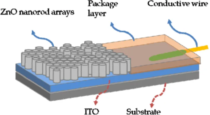
In this study, zinc oxide nanorod arrays were deposited on indium tin oxide (ITO) glass substrate (see Fig. 1) by employing chemical bath deposition. The morphology and electrical properties of ZnO modified ITO electrode by alterning various growth time and hybrid concentration was discussed. The ITO electrodes with ZnO nanorods modified by using chemical bath deposition method provide excellent electron tranfer properties which could apply in the sensing electrode of glucose biosensor.
II. METHODOLOGY AND EQUIPMENT
A. Preparation of ZnO Seeds Layer
The fabrication of ZnO thin film was firstly coating ZnO seeds layers as a pretreatment. The seeds layer was obtained by spin coating method on ITO glass. The seeds layer solution was synthesized by 0.02M zinc acetate dehydrate
[Zn(CH3COO)2・2H2O] and 0.03M solidum hydroxide
(NaOH) in methanol (CH3OH) and stirred for 2 hours at 58℃.
Then the solution was cooled down at room temperature and the ZnO seeds layer was coated on the electrode. Repeat above steps four times to finish the pretreatment of ZnO seeds layer on the substrate.
B. Preparation of Modified Electrode
In this work, ZnO nanorods were modified on ITO electrode. Firstly, the zinc nitrate (Zn(NO3)2) mixed with
hexamethylene-tetramine (HMTA) which forms equal molar concentration ratio of 0.04M ZnO mixed aqueous solution. The glass-ITO-seeds sandwich structure was immersed in the solution that heated to 80℃ and stirred at 220 rpm for 30, 60, 90 and 180 min, respectively. To remove the residue on the surface, the modified ITO electrode was immersed in deionized water and was cleaned by ultra-sonic cleaner for 20 sec. Then the sample was baked to remove the water molecule. Repeat the above steps and change the concentration of Zn(NO3)2/HMTA mixed solution in 0.1M.
C. Preparation of the Electrolyte
In this step, the electrolyte was synthesized from 0.1M phosphate buffer solution (PBS), 1 mM Fe(CN)63-/4- and
0.1M KCl. Then GOD was dissolved in electrolyte and the GOD catalysis solution was obtained.
D. Measurement and Apparatus
The electrochemical experiments were performed on a 661a electrochemical workstation (CH Instruments, USA). All experiments were carried out with a modified electrode as the working electrode, a platinum wire as the auxiliary electrode, and a silver / silver chloride electrode (Ag/AgCl) as the reference electrode. Scanning electron microscopy (SEM) was performed with a JEOL 5410LV (JEOL Ltd., Japan); X-ray diffraction (XRD) were done with an X-ray diffractometer (Shimadzu, Japan) using a Cu Kα source (λ = 1.54060Å) at 30 kV, 15 mA in the range of 20° < 2θ < 70° at a scan rate of 6.0°/min.
III. RESULT AND DISCUSSION
A. Material Characteristics of ZnO Modified Electrode
As shown in Fig. 2, the XRD pattern shows that ITO substrate, ZnO seeds layer and ITO substrate with ZnO nanorods. Apparently, ITO substrate shows obvious diffraction peaks at 2θ = 30.68° and 35.76° of ITO thin film with the deposition at (2 2 2) and (4 0 0) direction. The results of XRD were shown that the peak of ZnO seeds layer was not obvious. It may be contributed to that the ZnO grain was so small that the seeds layer could not satisfy the Bragg's law which established constructive interference. The result was also consistent with Ji et al. [30] that seeds layer with thickness under 240 nm would not show obvious pattern in XRD spectrum at (002) direction.
increase of the concentration. Initially, the diameter of ZnO nanorod is thin and grow like a bundle individually, but as time increases, and the bottom of rod will contact with each other and forms into ZnO beam welding, and then grows into larger ZnO rod [31], as shown in Fig. 4.
Above discussion shows that the concentration of ZnO mixed aqueous solution is an important factor to determine the diameters of ZnO nanorods. In general, in low concentration (0.04M) could grow to the maximum 50 nm ZnO nanorods and in the high concentration (0.1M) could grow to about 200 ~ 400nm [31]. However, the increase in growth time can only increase the uniformity and density but not increase the diameter of nanorods [32].
B. Electrochemical Behavior of ZnO Modified ITO Electrode
The measurement result of cyclic voltammetry is shown in Fig. 5, for the bared ITO electrode and 0.04M Zn(NO3)2
solution in various deposition time where the ZnO seed layer modified on ITO glass has immersed in 0.1M Zn(NO3)2
solution for 3 hours is also shown in Fig. 5. The redox peaks of bared ITO electrode are at 0.31 V and 0.09 V and the redox peak to peak potential (ΔEp) is 0.22 V. This result comes
from the redox reaction of Fe(CN)63- in the solution. Because
ΔEp is inversely proportional to the electron transfer rate, therefore, the greater ΔEp is, the slower the electron transfer
rate in the solution [33]. This result is consistent with the research of Gomathi et al. [34] that bared ITO electrode possess a similar redox peak potential value. As the growth time increased for the lower concentration of ZnO aqueous solutuion, the current decreased slightly while ΔEp increased.
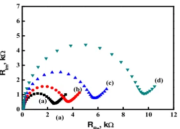
The reason could be contributed to that undopped ZnO semiconductor possess a poor electrical conductivity. However, the resistance of ZnO is increased after chemical bath deposition that matched with the results of electrochemical impedance spectroscopy (EIS) measurement, as shown in Fig. 6.
By the EIS measurements, the electron transfer impedance will increase as the growth time of ZnO nanorod increased, as shown in Fig. 6. Similar result has been observed by Zhai et al. [35], the diameter of ZnO nanorod increased as the electron transfer increased.
C. Characteristics of Biocatalysis on ZnO Modified Electrode
To confirm the catalytic activity of various ZnO nanorod, the modified electrode was immersed in 200 mg/dl glucose solution with an electrolyte that mixed by 1 mM Fe(CN)63-/4-
and 0.1M KCL. Table I shows the catalyst current in different ZnO growth time. The ΔIpa (mA) is the difference between
Ipa, G and Ipa, B, the variables of Ipa, B and, Ipa, G represent
oxidation peak currents in the absence and presence of glucose, respectively. As growth time increases, the catalytic current is slightly decreased. At a concentration of 0.04 M, and the growth time of 60 minutes, there is the best catalytic response current. This result shows that the ZnO nanorod is not the bigger the better, or the more compact the better. As the appropriate ZnO nanorod distance between each other, the specific surface area is increased that enhanced the catalytic current.
TABLE I
RESPONSE CURRENT OF VIROUS ZNONANORODS MODIFIED ITO ELECTRODE TABLE TYPE STYLES
Electrode Ipa, B Ipa, G ΔIpa Bare ITO 30.6 39.0 8.4 ZnO (0.04 M, 30 min) 24.7 34.6 9.9 ZnO (0.04 M, 60 min) 16.5 26.9 10.4 ZnO (0.04 M, 90 min) 16.2 19.7 3.5
Fig. 4. Mechanism of growing ZnO nanorods [33].
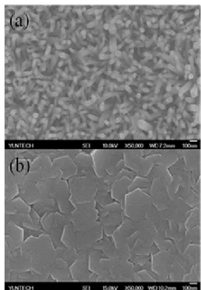
Fig. 3. FE-SEM images of ZnO nanorods: (a) 0.04 M, (b) 0.1 M for 90 min.
10 20 30 40 50 60 70 80
(d)
(c)
(b)
d
(400) (002)
(222)
In
te
n
si
ty
/(a
.u
.)
(d) large ZnO nanorods film (c) small ZnO nanorods film (b) ZnO seeds layer (a) bare ITO glass
2/(degree) (a)
IV. CONCLUSION
In this study, by controlling the mixed solution of ZnO concentration and the growth time of ZnO nanorod, the ITO electrode was successfully modified by various sizes of the ZnO nanorods. By electrochemical analysis, the small diameter of ZnO nanorods has a better catalyst current response where the best concentration of ZnO mixed aqueous solution is 0.04M and a growth time of 60 min. This means that the appropriate ZnO nanorods structure is an effective modification of ITO electrode surface and support great potential for glucose biosensor.
REFERENCES
[1] A. Qurashi, J. H. Kim, and Y.-B. Hahn, "Direct fabrication of ZnO nanorods array on-chip system in solution and their electrical properties," Electrochemistry Communications, vol. 18, pp. 88-91, 2012.
[2] A. Belaidi, T. Dittrich, D. Kieven, J. Tornow, K. Schwarzburg, M. Kunst, et al., "ZnO-nanorod arrays for solar cells with extremely thin sulfidic absorber," Solar Energy Materials and Solar Cells, vol. 93, pp. 1033-1036, 2009.
[3] O. Lupan, G. Chai, and L. Chow, "Novel hydrogen gas sensor based on single ZnO nanorod," Microelectronic Engineering, vol. 85, pp. 2220-2225, 2008.
[4] E. Fortunato, P. Barquinha, A. Pimentel, A. Gonçalves, A. Marques, L. Pereira, et al., "Recent advances in ZnO transparent thin film transistors," Thin Solid Films, vol. 487, pp. 205-211, 2005.
[5] N. K. Reddy, Q. Ahsanulhaq, and Y. B. Hahn, "Fabrication of zinc oxide nanorods based heterojunction devices using simple and economic chemical solution method," Applied Physics Letters, vol. 93, pp. 083124-3, 2008.
[6] A. Umar, M. M. Rahman, S. H. Kim, and Y. B. Hahn, "ZnO Nanonails: Synthesis and Their Application as Glucose Biosensor," Journal of
Nanoscience and Nanotechnology, vol. 8, pp. 3216-3221, 2008.
[7] S. K. Arya, S. Saha, J. E. Ramirez-Vick, V. Gupta, S. Bhansali, and S. P. Singh, "Recent advances in ZnO nanostructures and thin films for biosensor applications: Review," Analytica Chimica Acta, vol. 737, pp. 1-21, 2012.
[8] Y. Q. Fu, J. K. Luo, X. Y. Du, A. J. Flewitt, Y. Li, G. H. Markx, et al., "Recent developments on ZnO films for acoustic wave based bio-sensing and microfluidic applications: a review," Sensors and
Actuators B: Chemical, vol. 143, pp. 606-619, 2010.
[9] Y. Chen, D. M. Bagnall, H.-j. Koh, K.-t. Park, K. Hiraga, Z. Zhu, et al., "Plasma assisted molecular beam epitaxy of ZnO on c -plane sapphire: Growth and characterization," Journal of Applied Physics, vol. 84, pp. 3912-3918, 1998.
[10] M. Breedon, M. B. Rahmani, S.-H. Keshmiri, W. Wlodarski, and K. Kalantar-zadeh, "Aqueous synthesis of interconnected ZnO nanowires using spray pyrolysis deposited seed layers," Materials Letters, vol. 64, pp. 291-294, 2010.
[11] X. Liu, Q. Hu, Q. Wu, W. Zhang, Z. Fang, and Q. Xie, "Aligned ZnO nanorods: A useful film to fabricate amperometric glucose biosensor,"
Colloids and Surfaces B: Biointerfaces, vol. 74, pp. 154-158, 2009.
[12] T. Kong, Y. Chen, Y. Ye, K. Zhang, Z. Wang, and X. Wang, "An amperometric glucose biosensor based on the immobilization of glucose oxidase on the ZnO nanotubes," Sensors and Actuators B:
Chemical, vol. 138, pp. 344-350, 2009.
[13] Y. Zhang, Y. Zhang, H. Wang, B. Yan, G. Shen, and R. Yu, "An enzyme immobilization platform for biosensor designs of direct electrochemistry using flower-like ZnO crystals and nano-sized gold particles," Journal of Electroanalytical Chemistry, vol. 627, pp. 9-14, 2009.
[14] C. Xia, N. Wang, L. Lidong, and G. Lin, "Synthesis and characterization of waxberry-like microstructures ZnO for biosensors,"
Sensors and Actuators B: Chemical, vol. 129, pp. 268-273, 1/29/ 2008.
[15] Q. Ahsanulhaq, K. Jin-Hwan, and H. Yoon-Bong, "Controlled selective growth of ZnO nanorod arrays and their field emission properties," Nanotechnology, vol. 18, p. 485307, 2007.
[16] J. C. Johnson, H. Yan, R. D. Schaller, L. H. Haber, R. J. Saykally, and P. Yang, "Single Nanowire Lasers," The Journal of Physical Chemistry B, vol. 105, pp. 11387-11390, 2001.
[17] A. Qurashi, M. F. Hossain, M. Faiz, N. Tabet, M. W. Alam, and N. Koteeswara Reddy, "Fabrication of well-aligned and dumbbell-shaped hexagonal ZnO nanorod arrays and their dye sensitized solar cell applications," Journal of Alloys and Compounds, vol. 503, pp. L40-L43, 2010.
[18] T. Shinagawa, S. Watase, and M. Izaki, "Size-Controllable Growth of Vertical ZnO Nanorod Arrays by a Pd-Catalyzed Chemical Solution Process," Crystal Growth & Design, vol. 11, pp. 5533-5539, 2011. [19] C.-L. Hsu, S.-J. Chang, Y.-R. Lin, P.-C. Li, T.-S. Lin, S.-Y. Tsai, et al.,
"Ultraviolet photodetectors with low temperature synthesized vertical ZnO nanowires," Chemical Physics Letters, vol. 416, pp. 75-78, 2005. [20] D. Barreca, D. Bekermann, E. Comini, A. Devi, R. A. Fischer, A.
Gasparotto, et al., "1D ZnO nano-assemblies by Plasma-CVD as chemical sensors for flammable and toxic gases," Sensors and
Actuators B: Chemical, vol. 149, pp. 1-7, 2010.
[21] C. Zhang, "High-quality oriented ZnO films grown by sol–gel process assisted with ZnO seed layer," Journal of Physics and Chemistry of
Solids, vol. 71, pp. 364-369, 2010.
[22] J. H. Zheng, Q. Jiang, and J. S. Lian, "Synthesis and optical properties of flower-like ZnO nanorods by thermal evaporation method," Applied
Surface Science, vol. 257, pp. 5083-5087, 2011.
[23] D. C. Look, D. C. Reynolds, C. W. Litton, R. L. Jones, D. B. Eason, and G. Cantwell, "Characterization of homoepitaxial p-type ZnO grown by molecular beam epitaxy," Applied Physics Letters, vol. 81, pp. 1830-1832, 2002.
[24] O. Harnack, C. Pacholski, H. Weller, A. Yasuda, and J. M. Wessels, "Rectifying Behavior of Electrically Aligned ZnO Nanorods," Nano
Letters, vol. 3, pp. 1097-1101, 2003.
[25] Y. Tak and K. Yong, "Controlled Growth of Well-Aligned ZnO Nanorod Array Using a Novel Solution Method," The Journal of
Physical Chemistry B, vol. 109, pp. 19263-19269, 2005.
[26] L. Vayssieres, K. Keis, S.-E. Lindquist, and A. Hagfeldt, "Purpose-Built Anisotropic Metal Oxide Material: 3D Highly Oriented
0 2 4 6 8 10 12
0 1 2 3 4 5 6 7
(d)
(a)
(c) (b)
RRe, k
R Im
, k
(a)
Fig. 6. Electrochemical impedance spectroscopy (EIS) measurement results of various ZnO nanorods modified ITO electrodes in 1 mM Fe(CN)63-/4-and 0.1 M
KCl: (a) bare ITO; (b) ZnO (0.04 M for 30 min)/ITO; (c) ZnO (0.04 M for 60 min)/ITO; (d) ZnO (0.04 M for 90 min)/ITO.
Microrod Array of ZnO," The Journal of Physical Chemistry B, vol. 105, pp. 3350-3352, 2001.
[27] L. L. Yang, Q. X. Zhao, and M. Willander, "Size-controlled growth of well-aligned ZnO nanorod arrays with two-step chemical bath deposition method," Journal of Alloys and Compounds, vol. 469, pp. 623-629, 2009.
[28] C. Mu, Q. Zhao, D. Xu, Q. Zhuang, and Y. Shao, "Silicon Nanotube Array/Gold Electrode for Direct Electrochemistry of Cytochrome c," The Journal of Physical Chemistry B, vol. 111, pp. 1491-1495, 2007. [29] A. RIKLIN, E. KATZ, I. WILINER, A. STOCKER, and A. F.
BÜCKMANN, "Improving enzyme–electrode contacts by redox modification of cofactors," Nature, vol. 376, pp. 672-675, 1995. [30] L.-W. Ji, S.-M. Peng, J.-S. Wu, W.-S. Shih, C.-Z. Wu, and I. T. Tang,
"Effect of seed layer on the growth of well-aligned ZnO nanowires,"
Journal of Physics and Chemistry of Solids, vol. 70, pp. 1359-1362,
2009.
[31] Q. Li, V. Kumar, Y. Li, H. Zhang, T. J. Marks, and R. P. H. Chang, "Fabrication of ZnO Nanorods and Nanotubes in Aqueous Solutions,"
Chemistry of Materials, vol. 17, pp. 1001-1006, 2005.
[32] Z. Zhou, Y. Zhao, and Z. Cai, "Low-temperature growth of ZnO nanorods on PET fabrics with two-step hydrothermal method," Applied
Surface Science, vol. 256, pp. 4724-4728, 2010.
[33] S. Zhang, N. Wang, H. Yu, Y. Niu, and C. Sun, "Covalent attachment of glucose oxidase to an Au electrode modified with gold nanoparticles for use as glucose biosensor," Bioelectrochemistry, vol. 67, pp. 15-22, 2005.
[34] P. Gomathi, M. K. Kim, J. J. Park, D. Ragupathy, A. Rajendran, S. C. Lee, J. C. Kim, S. H. Lee, and H. D. Ghim, "Multiwalled carbon nanotubes grafted chitosan nanobiocomposite: A prosperous functional nanomaterials for glucose biosensor application," Sensors and
Actuators B: Chemical, vol. 155, pp. 897-902, 2011.
[35] Y. Zhai, S. Zhai, G. Chen, K. Zhang, Q. Yue, L. Wang, J. Liu, and J. Jia, "Effects of morphology of nanostructured ZnO on direct electrochemistry and biosensing properties of glucose oxidase,"