Microelectronics Journal 37 (2006) 1265–1270
SiO
2
single layer for reduction of the standing wave effects in the
interference lithography of deep photoresist structures on Si
Edson J. Carvalho
a,, Marco A.R. Alves
a, Edmundo S. Braga
a, Lucila Cescato
baFEEC-Unicamp, CxP 6101, 13083-970 Campinas, SP, Brazil bIFGW-Unicamp, CxP 6165, 13083-970 Campinas, SP, Brazil
Received 20 June 2006; accepted 18 July 2006 Available online 15 September 2006
Abstract
We demonstrate that the use of a single SiO2film, with thickness corresponding to one standing wave (SW) period allows the recording
of deep photoresist structures on silicon substrates by laser interference, without use of any additional antireflecting coating. This condition corresponds just to the opposite thickness (half SW period) previously proposed for using the SiO2films for phase-shifting the
SW pattern. Theoretical and experimental results demonstrated that for the lithography of deep structures, the contrast of the SW pattern, the minimum light intensity of the SW pattern and the photoresist adhesion are the most important parameters of the process. r2006 Elsevier Ltd. All rights reserved.
Keywords:Interference lithography; Standing wave pattern; Deep photoresist structures; RIE plasma etching
1. Introduction
Holographic or interference lithography is an interesting technique for recording periodic submicrometric structures in large areas. Many of these applications require the recording on silicon wafers [1–4]. Because of the high coherence of the laser light sources, employed in the interference lithography, the use of high reflectivity substrates generate serious problems to the lithography due to the presence of an additional interference fringe, parallel to the surface, called standing waves (SW). The effect may be so strong that impedes the lithography of photoresist films thicker than half of the SW period[5–7]. The alternative for reducing the SW contrast, offered by the photoresist manufacturers, is the use of bottom antireflective coatings (BARC)[8,9]. Such coatings provide a gradual refractive index variation between the photoresist and silicon, reducing the reflection and absorbing the transmitted light. There are also many materials proposed in the literature[10–12]that coated with the right thickness work as antireflecting (AR) coatings. The use of the
BARCs or ARCs, however, requires the introduction of one or more steps in the lithographic process.
Even if a photoresist film thinner than one period of the SW is used, there is a standing wave node at the interface photoresist substrate that causes an overcut profile at the bottom of the structure [6,13,14]. To modify the photoresist profile, Efremow et al.[6]proposed the use of a SiO2 film as a phase-shift layer. By using a SiO2
thickness equal to half period of the SW pattern, an undercut photoresist profile is obtained. However, no attention to the SW contrast was expended in this work because the employed photoresist thicknesses were smaller than one period.
In this paper, we study, theoretical and experimentally, the influence of thickness of the SiO2in the SW pattern in
the lithography of the deep photorresist structures, recorded by laser interference.
2. Theory
When a high reflectivity substrate is coated with a thin dielectric layer, the total-reflected wave is the sum of the wave reflected at the first interface and the multiple reflections inside the dielectric film[15]. The total reflection
www.elsevier.com/locate/mejo
0026-2692/$ - see front matterr2006 Elsevier Ltd. All rights reserved. doi:10.1016/j.mejo.2006.07.027
coefficient for such case is given by[15]
r¼ r01þr12e ij
1þr01r12eij
. (1)
r01being the reflection coefficient at the upper interface;r12
being the reflection coefficient at the interface dielectric
film-substrate and the phase difference j between the
multiple-reflected waves is given by:
j¼4p l0
n1tcosyd. (2)
n1 being the refractive index of the dielectric film; t its
thickness andydthe angle of incidence (inside the dielectric
film).
Assuming that the upper interface is formed by photoresist–SiO2, the bottom interface is SiO2–Si and the
incident light (l0¼457.9 nm) is linearly polarized in TE
direction we can calculate the total reflectanceðR¼ jrj2Þby using Eq. (1). For each incident angle, the reflectance is a
periodic function of the SiO2 film thickness. For an
incident angle inside the photoresist of yr¼7.881
(corre-sponding to a fringe periodL¼1mm), a refractive index of the unexposed photoresist nr¼1.67, a refractive index of
silicon oxiden1¼1.465 and a refractive index of the silicon
substrate N2¼4.599+i0.13051, the first maximum of
the reflectance occurs for a SiO2 film thickness of 79 nm
while the first minimum corresponds to the SiO2thickness
of 158 nm.
In Fig. 1 the reflectance is plotted as a function of the incident angle (yr), for the SiO2film thickness equal to 158
and 79 nm. In the same figure it is shown for comparison the reflectance for the single photoresist–Si interface. As it can be seen, from this figure, for theyrrange,
correspond-ing to frcorrespond-inge pattern periods NpLp0.36mm), the
reflectance for the SiO2 thickness of 158 nm is
approxi-mately constant and equal to the reflectance for the single photoresist–Si interface. This occurs because the refractive index of the SiO2 is lower than that of the photoresist.
A reduction of the reflectance is only possible if an AR dielectric film with refractive index higher than the photoresist is used[15].
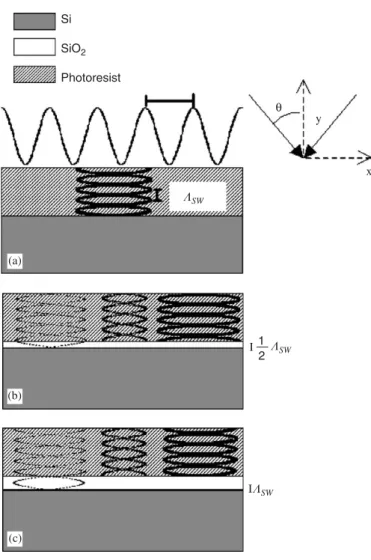
In the interference lithography, two laser beams reach the sample forming symmetric angles in relation to its normal (direction y in Fig. 2a). The interference light pattern inside the photoresist film is a superimposition of multiples waves in the two directions of incident beams and their respective reflections. The resulting irradiance inside the photoresist film is given by[5]:
I¼ ð1þ jrj2þ2jrjcosðkyyÞÞ
½ðI1þI2Þð1þmÞcosðkxxÞ, ð3Þ
I1 and I2 being the irradiances of the interfering beams
inside the photoresist,ris the total reflection coefficient at
1
0.8
0.6
0.4
0.2 0.4 0.6 0.8 1 1.2 1.4
θ
r [rad] Silicon Oxide t=79nm Silicon Oxide t=158nm Silicon
|r|
2
Fig. 1. Graphic of the reflectance |r|2as a function of incident angle inside the photoresist for three different substrates: (a) bare Si; (b) Si coated with a SiO2film thickness of 79 nm; and (c) Si coated with a SiO2film thickness
of 158 nm.
Si
SiO2
Photoresist
I SW
SW
1 2
ISW
y
x θ
(c) (b) (a)
Fig. 2. Scheme of the standing wave patterns generated, inside the photoresist, by the waves reflected: (a) at the Si substrate; (b), at a SiO2
film with 79 nm thickness; and (c) at a SiO2film with 158 nm thickness.
The left pattern corresponds to the standing wave assuming only the reflection at the interface SiO2–Si. The central pattern is generated by the
reflection at the photoresist–SiO2 interface and the right pattern
corresponds to the actual standing wave pattern, resulting by the sum of all reflected waves in the photoresist. Note that the pattern generated by the photoresist–SiO2interface is in phase with the pattern generated by the
reflection at the SiO2–Si for the SiO2 film thickness of 79 nm and in
the interface photoresist–substrate, and the fringe contrast mis defined as
m¼2
ffiffiffiffiffiffiffiffiffi
I1I2 p
I1þI2
. (4)
The first term in Eq. (3) corresponds to the SW pattern that is parallel to the surface (directionx in Fig. 2a) and has a periodLS, while the second term corresponds to the
principal fringe pattern, perpendicular to the surface
(direction y in Fig. 2a) and whose period is L. Both
periods are obtained from Eq. (3) by
kx¼
2p
L ¼
4p l0
nr sinðyrÞ ¼
4p l0
sinðyÞ, (5)
ky¼
2p
LSW¼
4p l0
nr cosðyrÞ, (6)
withnr being the photoresist refractive index, l0the laser
wavelength in vacuum andy andyr the half angle formed
between the incident beams in air and inside the photoresist film, respectively.
The angle yr¼7.881 (corresponding to a fringe period
L¼1mm), marked in the graphic of Fig. 1 as a dotted vertical line, corresponds to a SW period LSW¼158 nm
(inside the SiO2). Note that the minimum of the total
reflectance occurs just for this thickness of the SiO2 film
while the maximum of the reflectance occurs just for the
thickness proposed by Efremow [6] of half SW period
(79 nm).
The variation of the Reflectance, due to the different SiO2film thickness, changes the contrast of theSWpattern
and the minimum light intensity at the nodal planes. Considering only the first term in Eq. (3) we can define the contrast of the SW as
CSW¼
2jrj
1þ jrj2. (7)
The minimum light intensity at the nodal plane corresponding to the two SiO2 film thicknesses (79 and
158 nm) is, respectively (from Eq. (3)):
Imin¼0:185½ðI1þI2Þð1þmÞcosðkxxÞ (8)
and
Imin¼0:28½ðI1þI2Þð1þmÞcosðkxxÞ. (9)
Table 1resume the values for the SW contrast (Eq. (7)) and the values of the SW minimum light intensity, for the
two SiO2thicknesses. Note that, although there is a small
variation in the contrast of about 12%, the SW minimum light intensity changes of about 45%.
The scheme shown in Fig. 2illustrates the effect of the contrast and of the phase shift in the SW pattern inside the photoresist film. Fig. 2a shows SW pattern for the bare silicon substrate, that presents a node at the interface photoresist–Si because nroN2. Figs. 2b and c show the
scheme of the SW for the SiO2 thicknesses of 79 and
158 nm, respectively. In these cases the resulting SW pattern (Eq. (3)) may be decomposed in a pattern formed by the waves reflected at the photoresist–SiO2interface and
a pattern due the waves reflected at the SiO2–Si interface.
Note that the pattern formed by waves reflected at the photoresist–SiO2 interface always present a anti-node at
this interface, because nr4n1, while the phase shift of the
pattern formed by the reflection at SiO2–Si interface
depends on the SiO2thickness. For the thicknesst¼79 nm
(Fig. 2b), although the SW pattern has an anti-node at the interface (as proposed by Efremow et al. [6]to obtain an undercut photoresist profile), the patterns are in phase, increasing the contrast of the resulting SW pattern. For the SiO2 thickness t¼158 nm (Fig. 2c), the patterns are
counter phased decreasing the contrast of the resulting SW pattern, but with a node at the interface (resulting in an overcut photoresist profile).
3. Experiment
In order to verify experimentally the effect of the SiO2
film thickness on the SW in the interference lithography, similar exposures and development were performed using the photoresist Hoechst AZ 1518, diluted 1:1 in AZ thinner. The photoresist was spin coated on bare Si
substrates and on SiO2 films thicknesses of 72 and
157.4 nm, thermally grown in Si substrates.
The samples were, pre-baked at 701C for 20 min and
then exposed to a fringe-locked holographic interference pattern[16], using the linel¼457.9 nm of an Ar laser. The interference pattern period was L¼1mm, resulting in a semi-angle between the interfering beams in air of y¼13.241(in air) oryr¼7.881, inside the photoresist film.
For these experimental conditions and assuming a refractive index of the photoresist nr¼1.67, the period of
the SW inside the photoresist film will be (from Eq. (4)) LSW¼0.143mm and inside the SiO2 (n1¼1.465) will be
LSW¼0.158mm. The exposure dose was about 400 mJ/cm2,
and the development was done using MIF 312 diluted 1:1 in deionized water during 45 s.
For the recording of two-dimensional photoresist structures, a double holographic exposure was employed. In this case, after the first exposure of light energy dose of 380 mJ/cm2, the sample was rotated 901and exposed again
to the same light energy.
The cross-section of the recorded photoresist structures was analyzed by scanning electron microscopy (SEM).
Table 1
Theoretical values for the contrast of the SW pattern and minimum light intensity of the SW for the SiO2film with thickness of 79 and 158 nm
SiO2thickness
t¼79 nm (LSW/2) t¼158 nm (LSW)
CSW 0.86 0.77
4. Results and discussion
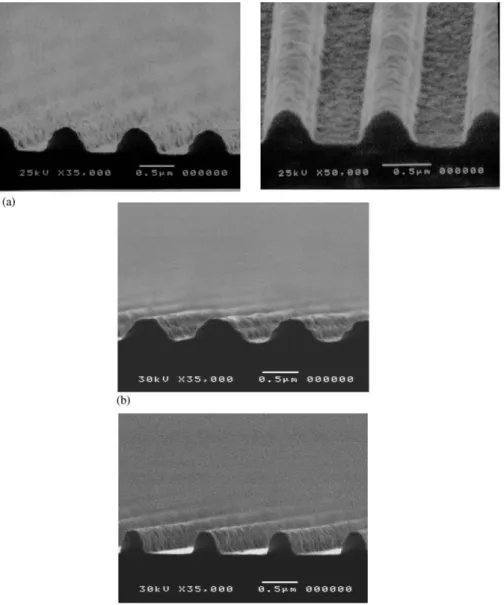
Fig. 3 shows the SEM photographs of the structures recorded in photoresist films with 300 nm of thickness, at the same conditions, on a bare silicon substrate (Fig. 3a), on a SiO2film with a thickness of 72 nm (Fig. 3b) and with
157.4 nm (Fig. 3c). These thicknesses of SiO2correspond to
approximately to the maximum and minimum contrast of SW pattern, calculated in Section 2 (Fig. 2). Although the variation in the contrast (12%) and in the light intensity minimum (45%) seems to be small, both effects together are responsible for the remarkable difference in the lithography between the photoresist structures shown in Figs. 3b and c. In particular, the minimum light intensity determines the capability of the developer to cross the SW nodal planes [17]. This effect is particularly amplified due to the non-linear behavior of the photoresist development ratio as a function of the exposure dose[17].
Note that the SiO2 thickness in Fig. 3b corresponds to
the presence of an anti-node of the SW pattern at the interface photoresist–SiO2(as proposed by Efremow et al.
[6] to phase-shift the SW pattern) while that of Fig. 3c corresponds to the presence of a node at the interface photoresist–SiO2 (as illustrated in Fig. 2). These results
clearly demonstrate that, for the recording of deep photoresist structures, the use of a SiO2 film thickness
equal to half period of the SW is not appropriate. By the other hand, as the deep photoresist structures present multiple SW periods, the phase shift of the SW does not change the profile. The unique effect of this phase shift would be a small change in the dimensions of the base of the recorded structures.
It can be observed also that the photoresist structure recorded on the SiO2film thickness of 157.4 nm (Fig. 3c)
presents a much better definition in the opened
channels than that recorded on bare silicon (Fig. 3a). The
photoresist structure on the bare Si substrate presents a larger width and an enlargement of the microscopy (Fig. 3a) shows the presence of a roughness on the bottom, indicating the presence of residual photoresist. The better definition in the opened channels in the photoresist structures on SiO2 film thickness of 157.4 nm is quite
repetitive and cannot be explained by the theoretical results of Section 2. This fact indicates that the adhesion of photoresist on different substrates plays a fundamental hole in the photoresist lithography [18–21]. Nagata and Kawai [18] demonstrate that the adhesion of the photo-resist, when immersed in developer, is much better on Si than on SiO2 films. This fact explains the much better
quality of the lithography on SiO2 films (Fig. 3c) in
comparison to that on Si (Fig. 3a). The poor photoresist adhesion on SiO2is responsible for the complete removal
of the thin unexposed photoresist layer at the interface photoresist–SiO2(bottom of the structures).
To demonstrate the feasibility of the interference lithography on Si substrates using SiO2 film thickness of
one SW period, we recorded both one (Fig. 4a) and
two-dimensional (Fig. 4b) deeper photoresist structures
(700 nm). Note that the ripple caused by the SW pattern is better defined in the two-dimensional structure because it was exposed to the interference pattern twice. Besides the ripple, the lithography of two-dimensional structures on SiO2 films with the thickness equal to one period of SW
pattern is always successful while it does not work for the bare Si substrates and different SiO2film thicknesses.
Fig. 4c shows a low-magnification microscopy of the array of photoresist structures that exhibits clear bottom surface around the structures. The view of the array show also the uniformity of the structures that remains un-changed in all recorded area of about 1pol2.Figs. 4d and e show the structures lithographed in the SiO2layer, by RIE
with CF4(for 20 min with a RF power of 50 W), using the
Fig. 4. One- and two-dimensional structures recorded in AZ 1518 photoresist on SiO2films with 157.4 nm, grown on silicon substrates and corresponding
patterns transferred to the SiO2 by RIE with CF4. (a) One-dimensional photoresist structure; (b) two-dimensional photoresist structure; (c) low
photoresist structures of Figs. 4a and b as masks, respectively.
5. Conclusion
We reported the use of a single SiO2 thermally
grown layer with a thickness equal to one period of the SW pattern to improve the interference litho-graphy of deep photoresist structures on silicon sub-strates.
We demonstrated that for the recording of deep photoresist structures, the phase shift of the SW pattern is not important, but the contrast of the SW pattern allied with the light intensity minimum are responsible for a remarkable difference in the lithography on Si substrates with different SiO2thickness. In particular, the minimum
light intensity determines the capability of the developer to cross the SW nodal planes.
Due to the small variations of the total reflectance
with the incident angle for the thickness of SiO2
equal to one period of the SW pattern, this same SiO2
film thickness can be used to record a wide range of fringe periods.
Although the contrast of the SW pattern, as well as the minimum light intensity are the same for bare silicon wafers and for SiO2 films with thickness equal to one
period of SW, the different adhesion of the photoresist on the SiO2and on Si explains the remarkable difference in the
quality of the lithography for both cases.
The use of a single SiO2 layer with a right
thick-ness instead of BARs or ARs simplifies the entire process and is fully compatible with the VLSI technologies
because: the SiO2 can be thermally grown on silicon
substrate; the SiO2can be patterned using the photoresist
as mask; and the SiO2pattern is a good mask for etching
the Si.
Acknowledgment
We acknowledge the financial support of the Fundac-a˜o de Amparo a Pesquisa do Estado de Sa˜o Paulo (FAPESP) and the Conselho Nacional de Pesquisa (CNPq).
References
[1] W. Ng, C.S. Hong, A. Yariv, IEEE Trans. Electron Devices 25 (1978) 1193.
[2] M. Campbell, D.N. Sharp, M.T. Harrison, R.G. Denning, A.J. Turberfield, Nature 404 (2000) 53.
[3] J.O. Choi, H.S. Jeong, D.G. Pflug, A.I. Akinwande, H.I. Smith, Appl. Phys. Lett. 74 (1999) 3050.
[4] W. Chen, S.H. Zaidi, S.R. Brueck, D.J. Devine, J. Vac. Sci. Technol. B 14 (5) (1996) 3339.
[5] S.H. Zaidi, S.R.J. Brueck, Appl. Opt. 27 (14) (1988) 2999.
[6] N.N. Efremow, N.P. Economou, K. Bezjian, S.S. Dana, H.I. Smith, J. Vac. Sci. Technol. B 19 (4) (1981) 1234.
[7] R.J. Lang, B. Smilowitz, IEEE Trans Sonics Ultrasonics 27 (3) (1980) 134.
[8] Clariant:http://www.azresist.com. [9] Shippley:http://www.chestech.co.uk/
[10] M.L. Schattenburg, R.J. Aucoin, R.C. Fleming, J. Vac. Sci. Technol. B 13 (6) (1995) 3007.
[11] H.L. Chen, T.C. Chu, M.Y. Li, F.H. Ko, H.C. Cheng, T.Y. Huang, J. Vac. Sci. Technol. B 19 (6) (2001) 2381.
[12] R.G. Ahrens, D.M. Tennant, Microelectron. Eng. 35 (1997) 229. [13] H.J. Lezec, E.H. Anderson, H.I. Smith, J. Vac. Sci. Technol. B 1 (14)
(1983) 1204.
[14] M.E. Walsh, Y. Hao, C.A. Ross, H.I. Smith, J Vac. Sci. Technol. B 18 (6) (2000) 3539.
[15] O.S. Heavens, Optical Properties of Thin Solid Films, Dover, New York, 1991.
[16] J. Frejlich, L. Cescato, G.F. Mendes, Appl. Opt. 27 (10) (1988) 1967. [17] B.A. Mello, I.F. Costa, C.R.A. Lima, L. Cescato, Appl. Opt. 34 (4)
(1995) 597.
[18] H. Nagata, A. Kawai, Jpn. J. Appl. Phys. 28 (10) (1989) 2137. [19] R.O. Lussow, J. Electrochem. Soc.: Solid State Sci. 115 (6) (1968)
660.
[20] A. Kawai, H. Nagata, H. Abe, M. Takata, Jpn. J. Appl. Phys. 30 (1) (1991) 121.