Electrical characterization of electronic interfaces to
communicate with electrogenic cells in vitro
Pedro Miguel Cavaco Carrilho dos Santos Inácio
Dissertação para obtenção do Grau Mestre em
Engenharia Eletrónica e de Telecomunicações
Orientador: Prof. Doutor Henrique Leonel Gomes (Universidade do Algarve) Coorientadora: Prof.ª Doutora Maria do Carmo Medeiros (Universidade de Coimbra)
iii
Electrical characterization of electronic interfaces to
communicate with electrogenic cells in vitro
Pedro Miguel Cavaco Carrilho dos Santos Inácio
Dissertação para obtenção do Grau Mestre em
Engenharia Eletrónica e de Telecomunicações
v
Electrical characterization of electronic interfaces to
communicate with electrogenic cells in vitro
“Declaração de autoria de trabalho”
Declaro ser o autor deste trabalho, que é original e inédito. Autores e trabalhos consultados estão devidamente citados no texto e constam da listagem de referências incluída.
Pedro Miguel Cavaco Carrilho dos Santos Inácio
______________________________________________________________
Copyright © aluno da Universidade do Algarve (UAlg), 2013
“A Universidade do Algarve tem o direito, perpétuo e sem limites geográficos, de arquivar e publicitar este trabalho através de exemplares impressos reproduzidos em papel ou de forma digital, ou por qualquer outro meio conhecido ou que venha a ser inventado, de o divulgar através de repositórios científicos e de admitir a sua cópia e distribuição com objetivos educacionais ou de investigação, não comerciais, desde que seja dado crédito ao autor e editor”.
vii
À Margarida,
Aos meus Pais
ix
Agradecimentos
A realização deste trabalho no âmbito da dissertação para obtenção do grau de Mestre em Engenharia Eletrónica e Telecomunicações constitui para mim uma honra, uma vez que me tem permitido aplicar os conhecimentos e competências, que adquiri nas várias disciplinas do Mestrado, enquanto desenvolvo um trabalho de investigação inserido no âmbito de um consórcio europeu, o iOne-FP7. Quero assim expressar o meu agradecimento ao meu orientador, Professor Doutor Henrique Leonel Gomes, pelo apoio, pela oportunidade e pelo convite para participar neste projeto, bem como por todo o acompanhamento e incentivo que sempre me tem transmitido; agradeço igualmente à Professora Doutora Maria do Carmo Medeiros, coorientadora neste trabalho, por toda a preciosa ajuda que facultou, pelo seu rigor e profissionalismo.
Agradeço ainda a todos aqueles que me têm acompanhado e que de alguma forma têm contribuído, quer na construção do meu conhecimento quer na minha formação como pessoa e profissional – aos meus colegas neste trabalho e a todos os professores nele envolvidos, pela amizade, apoio logístico e discussões; à Universidade do Algarve, aos técnicos e funcionários que, de alguma forma, deram o seu contributo para a construção dos dispositivos utilizados.
Quero ainda agradecer à Margarida pelo seu Amor, Doação, e Compromisso de partilha - obrigado pela dedicação em que eu me sinta sempre um homem feliz e realizado, e pela sua constante presença na minha vida! Agradeço também aos meus Pais, por terem sido incondicionalmente um alicerce firme na minha vida, transmitindo-me sempre a confiança e apoio nos transmitindo-melhores e piores motransmitindo-mentos e decisões da minha vida - obrigado pelo vosso Amor, Carinho, e Compromisso. Por último, agradeço à minha Família, que me ajudou a crescer e a tornar-me na pessoa que sou, partilhando muitos bons momentos da vida.
xi
Acknowledgments
The accomplishment of this dissertation for the degree of Master of Engineering Electronics and Telecommunications is an honor for me, since it has allowed me to apply the knowledge and skills that I acquired in the various disciplines of the Master, while developing a research inserted within a European consortium, the iOne-FP7. So I want to express my gratitude to my advisor, Professor Henrique Leonel Gomes, for the support, the opportunity and the invitation to participate in this project, as well as all the monitoring and encouragement that he has always transmitted; I am also grateful to Professor Maria do Carmo Medeiros, co-adviser in this work, all the precious help she has provided for his thoroughness and professionalism.
I am also grateful to those who have accompanied me and who somehow have contributed in the construction of my knowledge and in my training as a person and professional - my colleagues in this work and all the teachers involved in it, the friendship, logistical support and discussions; to the University of the Algarve, the technicians and staff who, somehow, have contributed to the construction of the devices used.
I would also like to thank Margarida for her love and commitment - thanks for the dedication that makes me feel always a happy and fulfilled man, and its constant presence in my life! I also thank my parents, for being unconditionally a firm foundation in my life, always passing me the trust and support in the best and worst moments and decisions of my life - thank you for your love, affection, and commitment. Finally, I thank my family, who helped me to grow and become the person I am, sharing many good moments of life.
xiii
Resumo
O presente documento reflete o trabalho realizado no âmbito do desenvolvimento de novos materiais eletrónicos biocompatíveis e biodegradáveis que veio permitir a construção de transístores implantáveis em seres vivos e capazes de comunicar com células nervosas (neurónios). Estes componentes eletrónicos serão capazes de reparar partes do tecido nervoso e restaurar a comunicação entre tecidos nervosos, por exemplo reparar lesões na medula espinal.
A motivação deste trabalho surge com a necessidade de desenvolver novos instrumentos que nos ajudam a perceber aspetos fundamentais da biologia, nomeadamente sobre como as células nervosas interatuam umas com as outras e respondem a estímulos elétricos e bioquímicos. Para tal, foi efetuada uma pesquisa que envolve vários aspetos, (i) a aplicação de materiais biocompatíveis com propriedades elétricas para a construção de transístores, (ii) estudo de processos eletroquímicos que ocorrem na interface entre o transdutor e a membrana celular, e (iii) a aquisição e estímulo de sinais bioelétricos.
No decorrer da investigação, foram caracterizados componentes eletrónicos capazes de operar em meios eletrolíticos complexos, nomeadamente, condensadores do tipo Metal-Isolador-Semicondutor (MIS); foram realizadas técnicas de medidas de ruído elétrico e análise espectral para a identificação de sinais bioelétricos, bem como foram obtidos e caracterizados os sinais bioelétricos produzidos por células quando submetidas a estímulos elétricos e bioquímicos extracelulares. Estas técnicas de medidas vêm comprovar a possibilidade de monitorizar a adesão das células e o seu estado de saúde, a sua atividade bioelétrica e o efeito provocado pela adição de estímulos extracelulares.
Palavras-chave: Biossensores; Bio eletrónica; Neuro-eletrónica; Biotransístor; técnicas de diagnóstico.
xv
Abstract
This document reflects the work done in the development of new electronic biocompatible and biodegradable materials that allow the construction of implantable transistors in living beings, able to communicate with nerve cells (neurons). These electronic components will be able to repair parts of the nervous tissue and restore communication between the nerve tissues, e.g. repair spinal cord injury.
The motivation of this work arises from the need to develop new instruments that help us understand fundamental aspects of biology, in particular on how nerve cells interact with each other and respond to electrical and biochemical stimuli. For this purpose, a search was performed involving various aspects, (i) applying biocompatible materials with electrical properties for constructing transistors, (ii) the study of electrochemical processes occurring at the interface between the transducer and the cell membrane, and (iii ) acquisition and stimulation of bioelectric signals.
During investigation were characterized electronic components capable of operating in complex electrolyte media, in particular, capacitors of the type Metal-Insulator-Semiconductor (MIS); electrical noise measurement techniques and spectral analysis for identifying bioelectrical signals were carried out, and were obtained and characterized the bioelectric signals produced by cells when subjected to electrical and extracellular biochemical stimulation. These technical measures prove the possibility to monitor the cells adhesion and their health state, their bioelectric activity and the effect caused by the addition of extracellular stimuli.
Keywords: Biosensors; Bioelectronics; Neuro-electronics; Biotransistor; diagnostic techniques.
xvii
Index
Agradecimentos --- ix Acknowledgments --- xi Resumo --- xiii Abstract --- xv Index --- xviiIndex of figure --- xix
Index of Tables --- xxi
Abbreviations --- xxii
CHAPTER 1 --- 1
INTRODUCTION 1 1.1 MOTIVATION AND OBJECTIVES ... 2
1.2 CONTRIBUTIONS ... 2
1.3 STRUCTURE OF THE THESIS ... 3
CHAPTER 2 --- 5
STATE OF THE ART 5 2.1 BIOELECTRONICS ... 5
2.2 BIOELECTRICDEVICES ... 6
2.2.1 INORGANICDEVICES ... 6
2.2.2 ORGANICBASEDTRANSISTORES ... 8
2.3 BIOELECTRICSIGNALS ... 11
2.4 ELECTRICNOISEINACELLMEMBRANE ... 13
2.4.1 THERMALNOISEINACELLMEMBRANE ... 14
2.4.2 INTRAMEMBRANARNOISE ... 16
2.4.3 THEMEMBRANEASABARRIERTOIONS ... 16
2.4.4 THEMEMBRANEASAWHITENOISEGENERATOR ... 17
2.4.5 NON-EQUILIBRIUMSITUATIONS(SHOTNOISE) ... 18
2.4.6 CHANNELNOISEVSPUMPNOISE ... 19
2.4.7 THEPOWERSPECTRALDENSITYOFCELLMEMBRANES ... 20
CHAPTER 3 --- 23
PETRI DISH AND CHIP HOLDER DEVICE 23 3.1 FEATURES ... 23
3.2 DESCRIPTION ... 24
3.3 PDCHSETUP ... 24
3.4 DIMENSIONS ... 26
3.5 FINAL VERSION RELEASE ... 27
CHAPTER 4 --- 29
EXPERIMENTAL SET-UP FOR ELECTRICAL MEASUREMENTS 29 4.1 EXPERIMENTALSET-UP ... 29
4.2 DATAACQUISITIONPROGRAM ... 31
4.3 PROCEDURESTOCARRYOUTLOW-LEVELANDLOWNOISE SIGNALS ... 34
4.3.1 PRE-AMPLIFICATION OF THE SIGNALS (CURRENT VS. VOLTAGE ... 34
4.3.2 SELECTINGPRE-AMPLIFIERBANDWIDTH ... 36
4.3.3 CONVERSION OF NOISE SPECTRAL DENSITY TO NOISE CURRENTSPECTRALDENSITY ... 37
4.4 CELLSCULTUREANDPROTOCOL ... 37
4.4.1 CRITERIAFORCELLSELECTION ... 38
4.4.2 CELLGROWTHONSENSINGDEVICE ... 39
CHAPTER 5 --- 41
RESULTS 41 5.2 EQUIVALENT MODEL FOR EXTRACELLULAR DEVICE INTERFACEWITHCELLSINVITRO ... 41
5.3 ELECTRICALMEASUREMENT ... 44
5.3.1 SMALL-SIGNALIMPEDANCETECHNIQUES ... 44
5.3.2 BIOELECTRONIC ACTIVITY UPON ELECTRICAL STIMULATION ... 47
5.3.3 SPECTRAL ANALYSIS OF THERMAL NOISE AND
xix 6.1 FUTUREWORK ... 61 REFERENCES --- 63
Index of figure
FIG. 1 – PHYSICAL STRUCTURE OF A TRANSISTOR FET‐EIS. ... 6 FIG. 2 – PHYSICAL STRUCTURE OF NWFET‐NT. ... 7 FIG. 3 – PHYSICAL STRUCTURE OF NWFET‐NT‐MGS. ... 8 FIG. 4 – PHYSICAL STRUCTURE OF THE DEVICE BASED ON ELECTRO POLYMERIZATION [21]. ... 9 FIG. 5 – PHYSICAL STRUCTURE OF THE DEVICE OECT. ... 10 FIG. 6 – SIMPLIFIED STRUCTURE OF A NEURON. ... 12 FIG. 7 – RC PARALLEL CIRCUIT ANALOGY WITH CELL MEMBRANE. ... 15 FIG. 8 – PUMPS AND CHANNEL OF CELL MEMBRANE STRUCTURE. ... 18 FIG. 9 – CHANNEL NOISE VS.PUMPS NOISE. ... 19 FIG. 10 – PDCH PARTS. ... 24 FIG. 11 – SCHEMATIC DESCRIPTION OF THE STEPS NEEDED TO BUILD THE PDCH. ... 25 FIG. 12 – PDCH BOTTOM BASE DIMENSIONS. ... 26 FIG. 13 – PDCH TOP BASE DIMENSIONS. ... 26 FIG. 14 – SCHEMATICS OF A PETRI DISH AND CHIP HOLDER (PDCH). ... 27 FIG. 15– (A) PHOTOGRAPH AND (B) SCHEMATIC DIAGRAM OF A SENSING DEVICE. ... 30 FIG. 16 – EXPERIMENTAL CONFIGURATION OF THE LABORATORY. ... 31FIG. 17 – FINAL VERSION OF AGILENT 35670A DYNAMIC SIGNAL ANALYSER ACQUISITION PROGRAM. ... 33
FIG. 18 – SPECIFICATIONS FOR SR570 AT LOW NOISE GAIN MODE. (A) AMPLIFIER BANDWIDTH AND (B) CURRENT NOISE AS FUNCTION OF FREQUENCY FOR SEVERAL SENSITIVITY SETTINGS. ... 36
FIG. 19 – OPTICAL PHOTOGRAPH OF C6 GLIAL CELLS IN CULTURE. ... 40
FIG. 20 – OPTICAL PHOTOGRAPH OF NEURONS (NEURO‐2A) IN CULTURE. ... 40
FIG. 21 – THE EQUIVALENT CIRCUIT OF METAL‐ELECTROLYTE INTERFACE [62]. ... 42
FIG. 22 – THE EQUIVALENT CIRCUIT MODEL OF SIGNAL PATHWAY IN THE SYSTEM. VIN: THE INTRACELLULAR POTENTIAL; CM AND RM: THE CAPACITY AND RESISTANCE OF CELLULAR MEMBRANE; JCE: THE JUNCTION BETWEEN THE CELL AND ELECTRODE; RM: THE SEALING RESISTANCE BETWEEN THE CELL AND DEVICE SURFACE; VX: THE POTENTIAL DIFFERENCE IMPOSED BY VG; VM: THE EXTRACELLULAR POTENTIAL DIFFERENCE RESULTED FROM VX AND VIN. ... 42
FIG. 24 – THE DL EFFECT IN A MEA DEVICE. (A) DIFFERENCE OF POTENTIAL IN SENSING DEVICE WITH AND WITHOUT CELLS
PRESENCE. (B) APPLICATION OF PERIODIC PULSE TRAIN IN PRESENCE OF C6 GLIAL CELLS. ... 43
FIG. 25 – TOP FIGURE SHOWS A SCHEMATIC DIAGRAM A CELL ON A SOLID SURFACE AND THE CORRESPONDING EQUIVALENT CIRCUIT THAT TAKES INTO ACCOUNT THE CELL AND THE ELECTROLYTE MEDIUM. BOTTOM FIGURE SHOWS THE IDEAL FREQUENCY DEPENDENCE OF THE CAPACITANCE AND LOSS OF SYSTEM. ... 45 FIG. 26 – CHANGES IN THE CAPACITANCE AND LOSS AS THE CELLS SEDIMENT AND ATTACH TO THE SENSING SURFACE. ... 46 FIG. 27 – CHANGES INDUCED IN THE CELL/ELECTRODE IMPEDANCE AFTER A TRAIN OF ELECTRICAL PULSES. ... 46 FIG. 28 – CHANGES INDUCED IN THE CELL/ELECTRODE IMPEDANCE REPRESENTED AS A LOSS TANGENT ... 46 FIG. 29 – THE BEHAVIOR OF THE LOSS AND THE CAPACITANCE WHEN THE SYSTEM HAS A HIGH DC CONDUCTANCE CAUSED BY THE ELECTROLYTE MEDIUM. ... 47 FIG. 30 – EXPERIMENTAL SET‐UP TO PULSE THE SENSING DEVICE WITH A TRAIN OF AC COUPLED VOLTAGES PULSES (ACROSS THE DIELECTRIC LAYER). ... 47 FIG. 31 – ELECTRIC CURRENT BEHAVIOUR PRODUCED BY DIFFERENT ELECTRICAL STIMULUS USING AC COUPLED VOLTAGE PULSE TRAIN, IN ORDER TO TRAIN C6 CELLS. ... 48 FIG. 32 – C6 GLIAL CELLS EXTRACELLULAR CURRENTS LEAKS DUE TO MEMBRANE CHARGES OVERLOAD. (A) . (B) NON‐PERIODIC RESPONSE. (C) PERIODIC RESPONSE. ... 49 FIG. 33 – TIME DEPENDENCE OF THE ELECTRICAL NOISE AFTER THE ADDITION OF CALCIUM, ELECTRICAL EXCITATION. ... 50 FIG. 34 – PERIODIC BURST OF NOISE WITH A FREQUENCY OF 0.2 HZ WERE OBSERVED AFTER CALCIUM ADDITION FOLLOWED BY AN ELECTRICAL STIMULUS. ... 50 FIG. 35 – CLOSE LOOK AT THE SHAPE OF THE NOISE AFTER THE ELECTRICAL STIMULATION AND ADDITION OF TTX. ... 51 FIG. 36 – CHANGES IN THE CURRENT FLUCTUATIONS MEASURED AFTER THE ADDITION KCL (30 M) TO NEURO2A CELLS. . 51 FIG. 37 – TIME TRACES OF THE CURRENT FLUCTUATIONS AFTER THE ADDITION OF KCL (30 M) TO NEURO2A CELLS. ... 52 FIG. 38 – EXPERIMENTAL SET‐UP TO PERFORM THERMAL NOISE AND BIOELECTRICAL SIGNALS MEASUREMENTS. ... 53 FIG. 39 – CURRENT POWER SPECTRAL DENSITY OF C6 CELLS DEPOSITED ON TOP OF GOLD SURFACES. ... 54 FIG. 40 – THE EFFECT OF ADDING DOPAMINE TO C6 CELLS ON THE NOISE SPECTRA. ... 54 FIG. 41 – HISTOGRAM OF TIME DEPENDENT TRACES AFTER THE ADDITION OF DOPAMINE. UPON ADDITION OF EXTRACELLULAR STIMULATION THE AVERAGE CURRENT MOVES TO LOWER VALUES WITH TIME. ... 55
FIG. 42 – CURRENT PSD OF C6 GLIAL CELLS DEPOSITED ON TOP OF GOLD MEA SURFACES. (A) FULL VIEW OF FREQUENCY RANGE. (B) ZOOM FOR FREQUENCIES RANGE 0.1 TO 100 HZ. (C) ZOOM FOR FREQUENCIES RANGE 0.1 TO 1 KHZ. ... 56
xxi
Index of Tables
TABLE I ‐ AUTOMATIC FREQUENCY RANGE MODE DEPENDENCY IN FUNCTION OF THE TIME WINDOW AND NUMBER OF SAMPLES. ... 32 TABLE II – NUMBER OF REAL DATA SAMPLES TO DOWNLOAD IN FUNCTION OF NUMBER OF SAMPLES SELECTED. ... 33 TABLE III – OPTIONS FOR PLOTTING FREQUENCY SPECTRUM WITH DIFFERENT UNITS. ... 33 TABLE IV – STANDARD RECOMMENDED PROCEDURE TO ACQUIRE A FREQUENCY RANGES USING DIFFERENT SENSITIVITIES LEVELS (IT IS RECOMMENDED TO USE AT LEAST 10 AVERAGES PER EACH FREQUENCY WINDOW). ... 37 TABLE V – SUMMARY OF ELECTRICAL TECHNIQUES AND TYPICAL SIGNAL SHAPES THAT PROVIDE INFORMATION ABOUT CELLS. 60Abbreviations
DL Double-Layer
ECPs Electrically Conducting Polymers
EDL Electrical Double Layer
EIS Electrolyte-Insulator-Substrate
FETs Field-Effect Transistors
GPIB General Purpose Interface Bus
ICS Intelligent Cell Surfaces
IHP Inner Helmholtz Plane
iONE-FP7 Implantable Organic Nano-Electronic – Seventh Framework Programme
MEAs Microelectrode Arrays
MGSs Micro Gold-Spines
MIS Metal-Insulator-Semiconductor
NTs Nanotubes
NWFETs Nanowire Field-Effect Transistors
NWs Nanowires
O-CSTs Organic Cell Stimulating and sensing Transistors OECTs Organic Electrochemical Transistors
OFETs Organic Field-Effect Transistors
OHP Outer Helmholtz Plane
OSCs Organic Semiconductors
OTFTs Organic Thin-Film-Transistors
PDCH Petri Dish and Chip Holder
PSD Power Spectrum Density
SWNTs Single-Wall Nanotubes
1
Chapter 1
INTRODUCTION
There are several pathologies that have lack of means to achieve its cure and / or better understanding. Hence raises the need to investigate the utility that micro and nano electronics technology can offer to biomedicine.
The root of this idea was born in 1780, the University of Bologna, when Luigi Galvani conducted a series of experiments that led the way for bio electrogenesis, relating the use of bioelectric forces with tissues of living organisms [1].
In [2], the author makes the analogy between computers and brains, noting that the common factor between them is working electrically; however, also notes that the large difference in mobility of ions in a solid structure of silica (about 103 cm2/Vs) and an aqueous structure (about 10-3 cm2/Vs) is the reason for the different operation of the architecture of the two information processors.
Thus, since the idea generated by L. Galvani, new horizons have arisen in research, looking for the development of an electrogenic interface. However, such knowledge generates knowledge, with the passage of time, new issues appear, in particular with regard to which material should be used to build such devices capable of implementing said electrogenic interface.
This work aims to characterize devices able to operate in complex electrolytic means. Thus, future research may find a solution to solve the complex problem presented earlier, the junction between the "brain" and "processor".
The idea of this project is based on the following key concepts: bioelectric interface, biocompatible implants electronic, acquisition and stimulation of biological signals.
1.1 Motivation and Objectives
The modern electronic displays today miniaturization of high quality; there are being developed nanometric devices that derive from organic and inorganic matter. Considering the fact that the growing demand for new ways of learning and research of biological media, from professionals in the biomedical area through the use of electronic equipment, there is a need and reason to develop electronic components capable of operating in complex electrolytic means, i.e., required to implement an interface between the biological environment and the computational means.
In order to achieve the development of an eletrogenic interface, were pre-determined the following objectives:
Characterization of electronic components capable of operating in complex electrolytic medium;
Performing measurements of electrical noise and spectral analysis for the identification of bioelectric signals;
Collection and characterization of bioelectric signals produced by cells when subjected to electrical and biochemical stimulus.
Another motivating factor is the fact that this project is inserted in a European consortium, the iOne-FP7, and the project intelligent cell surfaces (ICS) financed by Portuguese foundation for science and technology.
1.2 Contributions
The main contributions of this project are:
Developed of sensing devices in collaboration with Philips®.
Devices and knowledge imparted by the various partners of the European project iONE-FP7 and ICS.
3
1.3 Structure of the Thesis
This work is divided into 6 parts:
- The first consists of the introduction and Chapter 2, where it is reviewed the literature to support the development of this study (State of Art);
- Chapter 3 presents and develop holder able to support different electronic devices sensing devices with cell cultures in vitro;
- Chapter 4 presents the experimental set-up to record cells bioelectrical activity; - In chapter 5 presents the results and the respective critical analysis
- Finally, in Chapter 6, are identified conclusions and perspectives for future work to keep developing this project.
5
Chapter 2
STATE OF THE ART
In this chapter literature that supports this research is reviewed.
2.1 BIOELECTRONICS
Modern electronics started in 1947 with the appearance of the first transistor built based on inorganic semiconductors by Bardeen, Brattain and Shockley. In 1958, Jack Kirby built the first device with an integrated electronic circuit based on planar technology on a substrate of germanium [3], emerging as the way of the current micro-and nanoelectronics. Later, in 1977 Shirakawa, MacDiarmid micro-and Heeger developed the first organic semiconductor materials, the polyacetylene [4].
Recently based on advanced microelectronic devices, new ideas have emerged for application of electronic devices in biological media, such as suggested in [2], the analogy between the brain and a processor.
Thus began the generation of bioelectronics, based on two fronts, the devices based on organic and inorganic matter. Earlier, bioelectronic devices began to be studied to operate in different ways: in a first configuration, presupposed the monitoring of the devices performance in terms of potential, impedance, resistance, charge transport, among others, working as a support to knowledge effects in biological media devices while trying to figure out how to interact with biological media; in a second configuration, attempted to design bioelectronic devices for required functions, such as the biosensors [5].
However, the junction between the two configurations mentioned above determines the ultimate goal of bioelectronics, i.e, implementing an electrogenic interface capable of operating in complex biological media. This is also the focus of many research groups, working on developing electrogenic interfaces based on inorganic and organic materials.
2.2 BIOELECTRIC DEVICES
The raw metal electrodes that are typically used in active implantable devices are often associated to a poor stimulation and recording performance in the long term [27].
It is thus important the concern in developing bioelectrical devices that are biocompatible while maintaining good performance in the long term. For this purpose, the key is to use inorganic and organic matter as solutions for insulators and semiconductors.
Thus, this 2.2 point will be divided into two: the first shows the electrical devices developed based on inorganic matter, and the second, the devices developed based on organic matter.
2.2.1 INORGANIC DEVICES
Silicon (Si) is commonly used as a substrate for three reasons: (i) being an electrical conductor, which can be isolated with very thin layers of silicon dioxide (SiO2)
thickness ranging from 10 to 1000nm, thus making the silicon in a inert substrate perfect for cell culture, (ii) silicon dioxide suppress the transfer of electrons and prevent the electrochemical process leading to the etching of silicon, (iii) it is a technology well implemented in the marketplace, with high quality in microelectronics [2].
For these reasons, research groups have developed devices based on the same technology, are mostly devices based in transistors FET-EIS (Electrolyte-Insulator-Semiconductor) [6].
7
These electronic devices implement interfaces to cells, however are limited to functions as: sensibility to extracellular ion flow using ion-sensitive FET (ISFET) [2], acquisition of electrical and chemical signals [7], cell stimulation [8], cell adhesion [9] and [10], detection of cellular metabolism [11], among others.
Recently, new devices have been developed using nanotechnology such as nanowire FETs (NWFET) together with Nanotube (NT), verifying whether they have excellent performance in respect of predecessors FET transistors, with an average increase of transconductance from 45 to 800 nS, and an average increase of mobility from 30 to 560 cm2 / V.s [12].
Fig. 2 – Physical structure of NWFET-NT.
In Fig. 2, Source and Drain correspond to electrodes that lie on the insulator layer; in (a) Channel represents a nano layer between the electrodes, and (b) a layer which is much narrower than the electrodes; Nano-Tube is isolation between the channel layer and Electrolyte layer, which may it covers the entire channel or just part of it.
Several research works with devices that are based on the principles of NT-NWFET have been made for the application of nanotechnology to bioelectronics, as is the case of the application devices composed by NWs’s arrays for acquisition of biomolecular signal [13], or single-wall nanotubes (SWNT) devices for the acquisition of bioelectric signals [14].
In [15], there is an application of NWFET-NT that proves that the improvements in the acquisition of bioelectric signals, in relation to those previously obtained with FET-EIS devices. These improvements are due to the replacement of traditional metal contacts (electrodes) wide and flat (with hundreds of μm2), for electrodes with micro-spines (MGS), running these as tiny "needles" in which cells will become settled.
Fig. 3 – Physical structure of NWFET-NT-MGS.
In Fig. 3, it appears that the devices NWFET-NT-MGS have a physical structure similar to those mentioned in Fig. 1; however it is observed in (a) and (b) that electrodes of MGS-NT-NWFET are constituted by two layers, a conductive layer (the electrode) made of Pt, and another layer on the electrode which is insulator and made of silicon nitride (Si3N4), verifying that the MGS are physically connected to the electrode,
crossing perpendicularly the insulator layer. In (d), in a reduced scale, occurs the electroporation process that the MGS induce in cell membranes after a few cycles of polarization and hyperpolarization of the cell. In [15], is a study of cell behaviour in the presence of microelectrode arrays (MEAs).
However, devices with structures like those shown previously in Fig. 1, Fig. 2 and Fig. 3 wherein the substrates are Si and the insulating layer is an oxide (SiO2), are more
likely to contain defects, but also are extremely sensitive to alkali ions that often lead to oxide ruptures or hysteresis of devices [17], and is therefore very important the search for fusion devices based on organic matter (which will be presented below in section 2.2.2) and those presented at this point 2.2.1 [18].
9
applications in electronics today, among them Polyaniline (PANI), Poly(ethylenedioxythiophene) (PEDOT), Poly(phenylene vinylidene) (PPV), Poly(dialkylfluorene) (PDAF), Poly(thiophene) (PTs) and Poly(pyrrole) (PPy) [4]. In 1984 (Wrighton et al., 1984 cit. in [18]) developed the first transistor using organic material, an organic electrochemical transistor (OECT), thus initiating the new era of organic electronics.
The biggest advantages that organic devices present, compared to inorganic devices, come from low production costs through the use of printing techniques [19] and [20], as well as the ability to adjust the organic material properties for the intended purpose [18], while allowing the conjugation of polymers with substances such as drugs [1].
However, with the application of organic material to the bioelectrical devices, arises the problem of biocompatibility versus biodegradability [28], since the suitability of organic materials greatly differs, depending on the way they are synthesized and the overall nature of system conjugation with the substrate polymer, or its chemical composition, surface charge distribution and acidy [1].
Given these limitations it has been found that among various polymers, the PEDOT doped poly(styrenesulfonate) (PSS) forms a composition (PEDOT: PSS), which the quality of adhesion from cell culture closely resembles what happens in glass slides [1] such as seen by the investigation that explores the quality of the interaction from PEDOT with cell cultures in vitro [21].
In this study we performed a cell culture on an electrode, and after the accession of them, PEDOT was deposited in the saline solution (electrolyte medium), which already contained PSS and was involving the culture; this process is called electropolymerization.
In Fig. 4 is shown a device based on electropolymerization, demonstrating the simplicity and functionality of the electrical interaction between PEDOT and cells.
Also in [21] is referred that electropolymerization may become a future solution for fixing cells to an electrode; more recent studies [22] have confirmed that the creation of PPy or PEDOT nanotubes on electrodes promotes adhesion and cell proliferation.
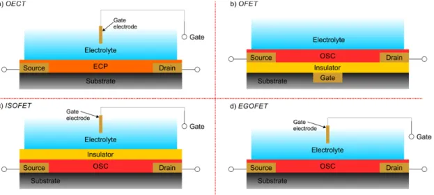
In [18] is a summary of various organic devices capable of operating in complex electrolytic medium which served as a base for the first interfaces with cells in vitro, such as: organic electrochemical transistor (OECT) ([29], [30] and [30]), organic transistor FET (OFET) ([17] and [23]), ion-sensitive transistor OFET (ISOFET) [34] and electrolyte-gated transistor OFET (EGOFET) ([35] [36]).
Fig. 5 – Physical structure of the device OECT.
Fig. 5 shows in (a) the physical structure of a OECT, being the operating principle based on the interaction of the conducting polymer layer (electrically conducting polymer - ECP) with electrolytic medium and cells.
Source and Drain terminals are merely representative and both are constituted by the ECP; differentiation in color comes from the possibility of existence of links with different metals to make connection to measurement instruments.
The gate terminal is introduced into the electrolytic medium intending to make changes in the conductivity of the ECP’s layer through the application of electric stimuli that lead to doping or non-doping the polymer. Recent studies found that an electrolytic medium containing PSS, or in the case of PEDOT being doped with PSS, it
11
In (b) is shown the physical structure of an OFET, and its working principle is very similar to the FET-EIS’s presented in paragraph 2.2.1, differing only in the layer of organic semiconductor (OSC) which lies on the insulator layer.
The OSC layer eases the production of FET devices, allowing design devices with different dielectric properties related to the combination OSC-insulator [18].
In (c) is shown the physical structure of an ISFET; these devices are adapted to explore the charges polarization, using the insulator layer in direct contact with the surrounding electrolyte medium.
Thus, using a top Gate, electrical potential may be induced on the OSC layer, i.e. current is modeled in Drain through the polarization of the charges in the OSB [18] and [34].
Finally, in (d) is shown the physical structure of an EGOFET, which the operating principle is based on the effect produced by the electrical double layer (EDL) formed by interfaces OSC-electrolyte and electrolyte-Gate.
Depending on the Gate’s polarization, ions are distributed to opposite interfaces, allowing current modulation in the Drain composed by OSC layer [18].
2.3 BIOELECTRIC SIGNALS
All biological systems are regulated by a multiplicity of electrical signals, and these assure the regulation of each cell functions and control the function of multicellular systems such as tissues and vital organs.
Inside an organism, these signals can be "transported" via either blood vessels or along neurons; in this case, the information transmission from one neuron to another is made by signals passing through the synaptic cleft [1].
The cell, the basic unit of any living tissue, presents an anatomy and physiology appropriate to her role. All cells present, along their membrane structure, a potential difference which is a difference in electric charge resulting from uneven load distribution between the region immediately adjacent to the interior and exterior of the cell membrane [33]; in the case of nerve cells, these are electrically excitable, which means that a stimulus produces a series of characteristic changes in resting potential, and their membranes can produce and conduct electrochemical impulses [33].
According to [18], is believed that the potential difference of the cell membrane responsible for producing and conducting electrochemical impulses is very important for the correct functioning of the cell.
The origin of said potential difference is in the excitement of the nerve cell, which in turn will generate the aforementioned pulse, also called bioelectrical signal, which will then propagate [18].
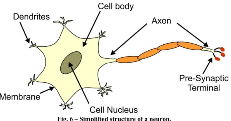
Fig. 6 – Simplified structure of a neuron.
In general, it can be said that a nerve cell is composed of four physiological units: dendrites, cell body, axon and presynaptic terminals.
Dendrites receive impulses from other cells, leading them to the cell body (structure where are the nucleus and other organelles); these impulses can be excitatory or inhibitory. The axon receives the bioelectric signal (pulse) from the cell body and transfers it to the next cell via pre-synaptic terminals ([26] and [32]).
The communication between neurons and from these to other tissues in the body is made via electrical signals called action potentials. These signals consist of brief, invariant and large electrical impulses and result from the application of a stimulus at a given point in the cell leading to depolarization, which reaches a designated by threshold level, in the membrane cell. The action potential is a major change in membrane potential that propagates without changing its amplitude, across the cell membrane ([32] and [33]).
13
At rest no current flows through the cell membrane. The neuron becomes excited when a local change in membrane potential occurs. If this change is above the threshold mentioned above, the neuron "fires" action potentials [32].
The number of action potentials is determined by the amplitude and duration of the input stimulus. So information transmitting is frequency-coded. Input stimuli can be received either from other neurons through the dendrites or by a direct physical or chemical stimulation, e.g. olfactory sensory neurons [32].
The neuron membrane is formed by a double layer of lipid molecules, and presents hydrophobic properties. Due to the chemical properties of these molecules, there is a separation of electrical charges across the membrane, which gives rise to differences in electrical potential transversely in the membrane; this is called the membrane potential [26].
2.4 ELECTRIC NOISE IN A CELL MEMBRANE
The possible effects that electromagnetic radiation emitted by high voltage power lines have on human health have been subject of discussion for some time now. Power frequencies of high voltage lines are low enough to interfere with cell membranes, which are highly resistant; thus, researchers have developed studies to assess the effect that the electric field induces in the membrane cells, comparing it with the proper electrical noise generated by the Brownian motion of the membrane.
Human exposure to electric fields is not new: since the dawn of human evolution, man has already been exposing himself to a slowly fluctuating field of about 100 V/m as he is moving around objects. However, with the high-voltage lines, the situation is different: almost all over the world there are giant metal structures that support a vast network of high voltage power lines that can carry up to half a million volts. When standing right under a power line a person can be exposed to about 10kV/m [37].
Many data have been gathered, analyzed, and reanalyzed over the last quarter century in order to understand the possible effects that exposure to these fields can cause to human health in the long term, but epidemiological studies have been somewhat inconclusive. The epidemiological inconclusiveness all the more justifies a biophysical approach: where and how does an electric field interact with a living
organism? Can we come up with some thresholds that have to be exceeded before a physiological effect can occur? [37]
Electromagnetic radiation has an electric and a magnetic component; following, the approach will be taken regarding possible physiological effects resulting from the electric component [37].
Living cells, by virtue of the underlying molecular processes, ion channel movements and dipole oscillations, exhibit intrinsic electric currents. (These currents have magnitudes on the order of a few femto to pico‐amperes (10‐15 to 10‐12). The
measurements of these currents reveal valuable knowledge of underlying biochemical, physiological and pathological processes [37].
The intracellular and extracellular medium is very ionic and conducts well. So when an electric field is imposed on a piece of living tissue, the ions move and, within a microsecond, compensate for the field inside the liquid [37].
The cell membrane is very resistive and this means that, once a steady state is reached, the entire voltage drop occurs across the cell membranes [37].
The significance of an added nanovolt‐order ELF oscillation across a cell membrane was first approached with rigorous quantitative physics in 1990 by Weaver and Astumian (WA) [37].
2.4.1 THERMAL NOISE IN A CELL MEMBRANE
Because of the Brownian motion of the charge carriers, there is always a small fluctuating voltage between the two ends of a resistor. This voltage was first measured and explained in 1928 by Johnson-Nyquist (JN). The so-called Johnson-Nyquist (JN) noise is white and in a frequency window of the average square voltage is expressed as:
〈∆ 〉
(1)where is the Boltzman constant 1.3806488 10 J/K , is the absolute temperature, is the resistance and Δ the bandwidth.
15
transmembrane noise can be evaluated as the noise between the capacitor plates in an RC parallel circuit (Fig. 7).
Fig. 7 – RC parallel circuit analogy with cell membrane.
In our context the resistor ( ) is also a white noise generator that follows Eq. (1). Because of the sheet-like nature of the membrane, the resistor R should then actually be conceived of as parallel resistors that each has a resistance , where is a very large number [37].
In 2002, W.T. Kaune put forward that, as a membrane protein is embedded in the cell membrane, it should, in the context of Fig. 7, be imagined to be inside the resistor [37].
Inside the resistor a protein should be subject to the electric field that presumably cause the JN-voltage of Eq. (1). Moving the protein from between the capacitor plates to inside the resistor in Fig. 7 effectively inverts the WA picture. This means that at low frequencies the field inside the resistor gets balanced out by the counter voltage from the capacitor. At high frequency the capacitor cannot follow. So eventually the protein will only “feel” the fast oscillations with periods below the RC time. In such a model, there would be a possibility for the power frequency radiation to be “stick out” above the noise spectrum [37].
2.4.2 INTRAMEMBRANAR NOISE
A cellular membrane has a thickness of approximately 5 nm, and many billions of square nanometers of surface area; so compared to that shown in Fig. 7, the resistor represented is, in fact, a very thin sheet. Considering the small conductivity of a membrane, the sheet should be modeled as an array of many parallel resistors. Taking, in that case, parallel resistors of resistance leads to the same net resistance . The amount of noise, however, increases very fast with , and not only does the number of “noise making resistors” increase when is increased, the amount of noise per resistor also grows with as each individual resistors generates a voltage that follows Eq. 2.
〈∆ 〉
(2)At each frequency the oscillations have random phase differences relative to each other. This being out of phase leads to the resistors pushing and pulling current in and out of each other. The capacitor is not involved in this “pulling and pushing” of current, which current constitutes the intramembranous noise. The intramembranous noise increases with and for large , the effect of the capacitor becomes increasingly more negligible [37].
An exact mathematical solution for a value of was first formulated by Vincze, Szasz, and Sazasz (Vincze, Szasz, and Sazasz, 2005, cit in [37]). A simpler derivation of the same result is found in [37]. When cutting up the membrane into the aforementioned individual resistors, a logical choice is taking the elementary resistor as a cube of 5nm x 5nm x 5nm. For an ordinary cell, this leads to a value of of the order of millions. The noise that a membrane protein “feels” in this case is almost all intramembrane, it is many times larger than what WA would predict, and the spectrum is effectively white [37].
2.4.3 THE MEMBRANE AS A BARRIER TO IONS
As mentioned before, a cellular membrane is the most part, a lipid bilayer with no mobile charges inside. The transmembrane voltage emerges because of penetrations of
17
A real membrane is also a capacitor, so any charge imbalance leads to a finite ΔV and a force, proportional to ΔV, that drives ΔV back to zero. This leads to an Ornstein– Uhlenbeck process (i.e. a random walk in a parabolic potential). These ions are not fixed at one position on the membrane-liquid interface, they move over the surface with a speed that can be estimated from 1 2⁄ , and comes out to be between 10 and 10 m/s [37].
2.4.4 THE MEMBRANE AS A WHITE NOISE GENERATOR
The dimensions that we took before for an elementary resistor (5nm × 5nm × 5nm) are also realistic for a membrane protein. Whenever an ion, on its trajectory on the membrane, crosses over such a protein, the protein feels a delta function-like electric pulse. Given the 3 ions per square micrometer (μ ) and the speed of these ions, the noise intensity that a membrane protein is subjected to due to the membrane-parallel random trajectories can be evaluated (Bier, 2005, cit in [37]). This noise comes out to be many orders of magnitude larger that the noise intensity due to the membrane transverse penetrations [37].
Transmembrane voltage fluctuations due to 2-sided shot noise at equilibrium were given by Eq. (1). This leads to a current power spectral density of (DeFelice, 1981, cit in [37]).
/
(3)The current power spectral density gives the mean square current per unit of bandwidth (i.e. Hz). The noise power in a certain frequency window is obtained by multiplying the power spectral density with the resistance and integration over the frequency window. The intensity of equilibrium noise is generally taken to be frequency independent. This “white noise” assumption is reasonable when working in a sub-MHz regime. (Bier, 2005 and DeFelice, 1981, cit in [37])
2.4.5 NON-EQUILIBRIUM SITUATIONS (SHOT NOISE)
For a living cell there is a continuous cycling of ions across the membrane as shown in Fig. 8. For each type of ion at steady state the same current I go in-to-out as well as out-to-in. In a living cell maintains electric currents across its membrane. Pumps drive ions against the electrochemical potential and channels let ions flow back. Transport through pumps “is” active and one-by-one. Channels let about 10 ions pass during an average channel opening. The randomness of the channel openings is the main contributor to non-equilibrium noise [37].
Fig. 8 – Pumps and channel of cell membrane structure.
Pumps drive ions through the membrane against the electrochemical gradient. This active transport requires energy and is commonly powered by the hydrolysis of ATP. Ion channels allow ions to flow with the electrochemical gradient. Pumps transport ions one-by-one. When the actual membrane passage time of an ion is negligible compared to the time between subsequent passages, we can think of these passages as delta function-like pulses. We then face ordinary shot noise [37].
The noise is white and the current power spectral density is easily evaluated as (DeFelice, 1981, cit in [37]):
(4)
19
corresponds to about 10 elementary charges per second. So during an average channel opening about 10 ions flow [37].
The current power spectral density due to channel activity is given by
(5) There is a prefactor 4 instead of a prefactor 2 because the open time of a millisecond
is an average of an exponential distribution [37].
2.4.6 CHANNEL NOISE VS PUMP NOISE
Channel noise is larger than the pump noise by a factor of about ten thousand. This is basically because pumps transport charge in larger units. So we have .
Fig. 9 – Channel noise vs.Pumps noise.
In Fig. 9, the measured power spectral density of noise across a cell membrane behaves like 1⁄ between about 10 and about 10 . Above 10 the level of the white equilibrium noise starts to exceed the non-equilibrium noise. The measured plateau where is smaller than about 10 corresponds well with our estimate from Eq. (7). At the power frequencies the non-equilibrium noise is about 100 times as intense as the equilibrium noise [37].
(6) Eq. (6) is a valid approximation as long as one looks at frequencies smaller than the
channel’s inverse average open time. At frequencies higher than 1⁄ , the correlations on time scales shorter than make for a smaller noise amplitude. When one type of channel is involved, the eventual spectrum is a sigmoid; a
so-called Lorentzian spectrum that drops down from 4 to zero at about 1⁄ [37].
2.4.7 THE POWER SPECTRAL DENSITY OF CELL
MEMBRANES
The power spectral density of actual cell membranes was first recorded in the 1960s by Verveen and Derksen (Verveen, 1966 and Derksen, 1965, cit in [37]). More accurate recordings have been made since (Diba, Lester and Koch, 2004 cit in [37]). The equation depicts the general shape of such spectra:
⁄ (7)
The plateau that runs from zero Hz to somewhere between 1 and 10 Hz represents the level 4 that we just calculated. Verveen and Derksen already noticed that this level was many times larger than what just equilibrium noise would predict. For the dimensionless ratio between non-equilibrium and equilibrium noise we derive as given in the equation [37].
For the current power spectral density of the equilibrium noise we ignore the intramembrane noise and took the WA estimate. Substituting realistic values for the resistance of a cell membrane we find for a value of about 1000. To the right of the plateau the power spectral density drops off roughly like 1⁄ . The apparent 1⁄ -noise can be explained by the fact that, in a real cell membrane, there are many types of channels with different ’s and different ensuing values of . The 1⁄ pattern can thus emerge as a superposition of a number of Lorentzians. It has been argued that channels may exhibit 1⁄ noise in and of themselves (Bassingthwaighte, 1994, cit in [37]), but these ideas are still controversial.
At the power frequency we still have a ratio Snoneq/Seq of about one hundred.
Experimental observations affirm this (Derksen and Verveen, 1966; Diba, Lester and Koch, 2004 cit in [37]). As the according to the WA model already overwhelms
21
2.4.8 NOISE IN NERVE CELLS
Some non-equilibrium noise may not just be noise, but actually a signal. This is most obvious with a signal going through a nerve cell. In that case a signal propagates as the opening of sodium channels triggers the opening of nearby sodium channels. These channel openings are regulated and they no longer constitute noise, but, instead, make up a signal that moves information [37].
With non-equilibrium noise in living systems we face a gray area between signal and noise [37].
23
Chapter 3
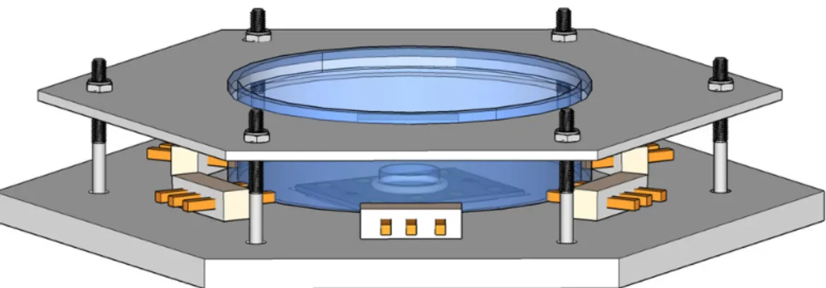
PETRI DISH AND CHIP HOLDER DEVICE
In this chapter, will be described a sensing device, designed by me in collaboration with members of the team involved in this project, capable to perform electronic measurements in biological environmental in vitro.
3.1 Features
- Transparent and biocompatible device capable to perform advanced measurements in biological environments.
- Uses of standard size Petri Dish produced by SARSTEDT®1: o Resistance up to 80º
o Made from transparent polystyrene
o Dimension of 35 10 , gamma-sterile proper for ventilation cam with 5 of working volume
- Uses of standard O-ring standard sizes and biocompatible2.
- Metal screws with 16 length and 2 diameter, combined with adapted nuts in order to perform strength between top and bottom bases.
- Metallic gold (Au) plated pins, to perform instrument and device connection.
- Device chassis made in extrude acrylic, resistant up to 70° for long period of use, and electrical characteristics: dielectric constant at 50Hz about 3.7, volume resistivity of 10 Ω. and surface resistivity of 10 Ω 3.
1 http://www.sarstedt.com, available at 23/07/2013. 2 http://www.prepol.com/, available at 23/07/2013. 3 http://www.dagol.pt/uk/, available at 23/07/2013.
3.2 Description
The device Petri Dish and Chip Holder (PDCH) are general propose devices to perform cells culture in vitro in the top of electronic sensing devices, capable to contain 5ml of working volume approximately, and operate in biological environment as so incubator environment, where atmosphere is about 37° .
That device is designed exclusively for Philips® electronic devices (chip), but can be redesigned for others. The reason is to perform a Chip Holder (CH) with the correct dimensions.
3.3 PDCH Setup
25
The followed scheme presented at Fig. 11, shows the different steps to assemble the sample holder with the sensing device. During the second process, it is needed to be done bindings between the device pads and the CH pins.
3.4 Dimensions
27
3.5 Final version release
The final prototype built of PDCH (see Fig. 14), was fabricated with transparent extruded acrylic. The Fig. 11 shows the different steps to assemble the PDCH.
29
Chapter 4
EXPERIMENTAL SET-UP FOR ELECTRICAL
MEASUREMENTS
The experimental set-up and the electronic instrumentation used to record electrical bioactivity of the cells in vitro are described in this chapter. The type of cells used is also briefly described.
4.1 EXPERIMENTAL SET-UP
To record the bioelectrical signals a noise measuring system was used [25]. A schematic diagram is shown in Fig. 16.
This system is comprised by an Agilent 35670A Dynamic Signal Analyzer, which operates together with a battery operated low-noise current pre-amplifier Stanford Research SR570. A Keithley 487 picoammeter with accuracy of 10fA and a Keithley 2182A digital nanovoltmeter and low voltage meter were also used to measured signals in a slow time scale. The entire measuring system together with the CO2 incubator was
placed in an iron shield with a dedicated electrical ground. The entire system is designed to eliminate parasitic interferences, particularly those caused by the 50 Hz main line.
Impedance measurements were carried out by a RCL meter a Fluke PM6306 Programmable Automatic RLC meter, with capabilities to measure Capacitance (C), Resistance (R) and Inductance (L), within the range of 10 Hz to 1 MHz.
Electrical stimulation of the cells in vitro was carried out by an Agilent 33220A Function / Arbitrary Waveform Generator.
The sensing devices are metal-insulator semiconductor field effect transistors (MISFETs) where the transistor channel is left empty. The living cells will fill the transistor channel. Fig. 15 shows a schematic diagram of a sensing device together with a photograph. The devices are comprised of gold microelectrode arrays spaced 10 microns (L=10 m) and with a channel width (W) of 10.000 m. The electrodes are on top of thermal oxidized silicon wafers. The oxide (SiO2) is 200 nm thick and the
substrate is a highly doped silicon wafer (resistance of 1 3 Ω. ). The oxide layer is used to couple AC signals to the junction SiO2/membrane.
In case of chemical stimuli, the method adopted in the laboratory was to add extracellular solutions such as: Calcium Chloride Dehydrate CaCl . 2H O), Potassium Chloride KCl and Dopamine.
In some cases, in order to verify that the signals measured were generated by cells and not artifacts, a neurotoxin was added to the cell culture, tetrodotoxin (TTX), which inhibits cells from producing action potential.
It is mandatory condition that a culture medium of cells in vitro has a sterile atmosphere and levels of oxygen (O2), carbon dioxide (CO2) and moisture controlled to
specific values.
Thus, all the experiments were performed inside of an incubator (Thermo Scientific Midi 40 Small Capacity CO2 Incubator, 120) that guarantees the maintaining of
sterilization and controlled atmosphere to carry out the experiments.
Fig. 15– (a) Photograph and (b) schematic diagram of a sensing device.
(a)
31
Fig. 16 – Experimental configuration of the laboratory.
In Fig. 16, it can be seen that all the measurement equipment have test leads loose, that should connect to the interface cable for the inside of incubator, in order to perform measurements.
4.2 DATA ACQUISITION PROGRAM
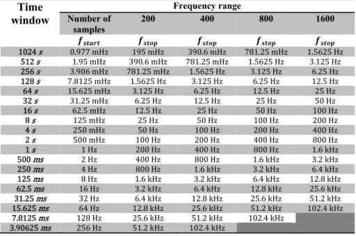
In order to provide better and efficient measurements, a program was developed to operate with the Agilent 35670A Dynamic Signal Analyzer. Fig. 17 is an illustration of the program main window. The interface used to connect instrument with the computer is GPIB-USB. Drivers are available at Agilent4 web site which is required to control the instrument. This program has the capability to extract and reconstruct the entire frequency spectrum using different time windows. This instrument is designed to
support 1, 2 or 4-channels, but the developed program only make uses of 1-channel in order to achieve a larger frequency span. The full range is from 122 to 102.4 . The frequency range can be set to automatic or manual, and the resolution lines (number of samples) per time window can be set to be within the range of 100, 200, 400, 800 or 1600 samples. By default, the instrument and the program uses automatic frequency mode (see Table I for automatic frequency span configuration options). In case of manual mode, the behavior of the frequency observation window depends of the start ( ) / stop ( ) frequency inserted. That means the final resolution ( ) will be as expressed in (8), where ( ) is the number of samples.
(8)
Table I - Automatic frequency range mode dependency in function of the time window and number of samples. Time window Frequency range Number of samples 200 400 800 1600 1024 s 0.977 mHz 195 mHz 390.6 mHz 781.25 mHz 1.5625 Hz 512 s 1.95 mHz 390.6 mHz 781.25 mHz 1.5625 Hz 3.125 Hz 256 s 3.906 mHz 781.25 mHz 1.5625 Hz 3.125 Hz 6.25 Hz 128 s 7.8125 mHz 1.5625 Hz 3.125 Hz 6.25 Hz 12.5 Hz 64 s 15.625 mHz 3.125 Hz 6.25 Hz 12.5 Hz 25 Hz 32 s 31.25 mHz 6.25 Hz 12.5 Hz 25 Hz 50 Hz 16 s 62.5 mHz 12.5 Hz 25 Hz 50 Hz 100 Hz 8 s 125 mHz 25 Hz 50 Hz 100 Hz 200 Hz 4 s 250 mHz 50 Hz 100 Hz 200 Hz 400 Hz 2 s 500 mHz 100 Hz 200 Hz 400 Hz 800 Hz 1 s 1 Hz 200 Hz 400 Hz 800 Hz 1.6 kHz 500 ms 2 Hz 400 Hz 800 Hz 1.6 kHz 3.2 kHz 250 ms 4 Hz 800 Hz 1.6 kHz 3.2 kHz 6.4 kHz 125 ms 8 Hz 1.6 kHz 3.2 kHz 6.4 kHz 12.8 kHz 62.5 ms 16 Hz 3.2 kHz 6.4 kHz 12.8 kHz 25.6 kHz 31.25 ms 32 Hz 6.4 kHz 12.8 kHz 25.6 kHz 51.2 kHz 15.625 ms 64 Hz 12.8 kHz 25.6 kHz 51.2 kHz 102.4 kHz 7.8125 ms 128 Hz 25.6 kHz 51.2 kHz 102.4 kHz 3.90625 ms 256 Hz 51.2 kHz 102.4 kHz
As a user option, the instrument can be configured with four plots at the same time. The program developed can be configured with only two plots at the same time, in frequency or time domain. However and as a consequence the download of the data from instrument via GPIB-USB can be longer when high resolution line is selected and/or two plots are activated at the same time (typically for 1600 samples per
33
Fig. 17 – Final version of Agilent 35670A Dynamic Signal Analyser acquisition program. Table II – Number of real data samples to download in function of number of samples selected.
Number of samples
Baseband
Frequency domain
data samples Time domain data samples
100 101 256
200 201 512
400 401 1024
800 801 2048
1600 1601 4096
Table III – Options for plotting frequency spectrum with different units.
Spectrum Units Voltage Voltage square Square Root Power Spectral Density ⁄√ Power Spectral Density ⁄ Energy Spectral Density . ⁄
4.3 PROCEDURES TO CARRY OUT LOW-LEVEL AND LOW
NOISE SIGNALS
4.3.1 PRE-AMPLIFICATION OF THE SIGNALS (CURRENT
vs. VOLTAGE
Signals can be amplified as voltage or current. The selection is made on the basis of the sample resistance.
A very important precaution is the overall noise figure ( ), which is the measuring unit widely used to noise performance quantification. The noise factor ( ) can be defined as in Eq. (9) [61].
(9)
and is the signal-to-noise ratio at the input and the output of the amplifier, respectively. represents the power gain of the amplifier, while and are the noise power at the input and output of the amplifier. In terms of mathematics, the is given by the noise factor expressed in , as in (10) [61].
(10) For a chain of amplifiers (as the case of multiple instruments connected in series) the
overall noise factor is expressed in Eq. (11) [61].
∑ (11)
is the noise factor provided from the first stage of amplification, and from then can be generalised for a chain of amplifiers, each one with noise factor of and a
35
current flowing through the sensing device, it also means that noise is generated by a random noise current source, which also depends from the resistance [25]. That is why the signal amplification decision is so important, because signals in baseband are predominantly dependent from thermal noise, which implies a pre-amplification stage implemented by low noise amplifier in order to reduce noise amplification. Having considering this, the most natural choice for amplifying the device output is to use a low noise current amplifier, even more for high resistance samples. The low noise current amplifier converts the output current noise into voltage, avoiding current to voltage conversions in the circuit which depend on other circuit parameters and therefore introduce errors [25].
The solution adopted to implement the first pre-amplification stage was to connect the experimental sensing device to a Stanford Research 570 (SR570), which is a commercial low-noise current pre-amplifier that operates with a battery to minimize the 50Hz power-line noise. The SR570 when is operating in low noise mode, allocates most of the gain in the front end of the instrument to decrease the magnitude of thermal noise (Johnson noise) at the output.
The final resolution of our measuring system is controlled by the resistance of the set formed by cells plus medium. For a typical value we usually have at low frequency resistance of 140 MΩ which gives a thermal noise of 2.318 ⁄ . This determines our detection limit (noise floor of our measuring system cells plus electrolyte).
4.3.2 SELECTING PRE-AMPLIFIER BANDWIDTH
As an option from the adopted instrument (SR570) to implement the pre-amplification stage, the sensitivity can be adjusted, although is an option that user should use with careful. By increasing the sensitivity, decreases the frequency bandwidth to be recorded, as a consequence of loose temporal resolution. In Fig. 18 is exemplified the relation between instrument amplification bandwidth and gain.
Fig. 18 – Specifications for SR570 at LOW NOISE gain mode. (a) Amplifier bandwidth and (b) current noise as function of frequency for several sensitivity settings.
Fig. 18 was retrieved from SR570 specifications manual5. The most important information that can be learned from Fig. 18 is the level of instrument noise floor for different sensitivity level, which means when instrument is set in LOW NOISE gain mode, for a given gain, the LOW NOISE mode allocates gain toward the front-end in order to quickly "lift" low-level signals.
The user can adjust the sensitivity within the range of 1 / to 1 / , which is displayed in instrument front-panel as the product of a factor 1, 2 or 5 and a multiplier (x1, x10, x100) with the appropriate units.
The best way to acquire data in a broad frequency range using the SR570, is to select the LOW NOISE gain mode, turn all the filters OFF (select NONE at instrument front-panel), and disable all the DC bias sources. Considering both current and bias voltage sources at OFF state, a standard recommended procedure to acquire a frequency ranges using different sensitivities levels, is the one described on table IV.
37
Table IV – Standard recommended procedure to acquire a frequency ranges using different sensitivities levels (It is recommended to use at least 10 averages per each frequency window).
Sensitivity Gain mode: LOW NOISE
Frequency Temporal
Window Resolution Window Resolution 1 µA/V 0 Hz ‐ 200 Hz 125 mHz 8 s 2 ms 1 µA/V 200 Hz ‐ 1 kHz 125 mHz 2 s 488 µs 1 µA/V 1 kHz ‐ 13.8 kHz 375 mHz 125 ms 30.5 µs 10 µA/V 13.8 kHz ‐ 26.6 kHz 7.5 Hz 125 ms 30.5 µs 10 µA/V 26.6 kHz ‐ 52.2 kHz 16 Hz 62.5 ms 15.25 µs 100 µA/V 52.2 kHz ‐ 103.4 kHz 32 Hz 31.25 ms 7.63 µs
All values for resolution calculation where taken in account that Agilent 35670A is selected for maximum temporal resolution; this means the number of samples considered are 1600 (which implies the measuring of 4096 samples in time domain, see Table II).
Another aspect to take into account is averaging. The use of averaging is not desirable when single events may occur.
4.3.3 CONVERSION OF NOISE SPECTRAL DENSITY TO
NOISE CURRENT SPECTRAL DENSITY
Due to the dynamic signal analyzer measures the noise spectral density in voltage units, mathematical calculations are needed in order to obtain the desired results of current noise spectral density. This is done using the following transformation.
⋅ (12)
where represents the noise measured by the analyzer expressed in ⁄√ and is the sensitivity of the amplifier [25].
4.4 CELLS CULTURE AND PROTOCOL
Two types of commercial available immortal cells cultures were used in this study: (i) C6 glial cells from Rattus norvegicus, rat, and (ii) Neuro-2A neuroblast cells from Mus muscullus, mouse. Optical photographs of the two types of cells are shown in (Fig. 19) and (Fig. 20) respectively.
4.4.1 CRITERIA FOR CELL SELECTION
Rat glioma C6 cells are glial cells from brain tissue, they are adherent cells [38], and their morphology is fibroblast. C6 glial cells are frequently used to study cellular functions and cell signalling. These cells have sodium channels, calcium channels and potassium channels [52]; furthermore they have receptors to neurotransmitters such as ionotropic glutamate receptors (GluRs) and ionotropic GABA receptors (GABAa and
GABAc) as well as glycine receptors [53][54].Glial cells are not electrically excitable,
however, they can generate intracellular Ca2+ waves travelling from one glial cell to the next [51]. Calcium signalling might thus be a form of glial excitability enabling these cells to integrate extracellular signals, communicate with each other and exchange information with neurons.
In excitable cells, the initiation of the cytoplasmic Ca2+ signal results from both Ca2+ entry via plasmalemmal voltage or ligand-gated Ca2+ channels and Ca2+ release from internal pools, while in non-excitable cells it is the release of Ca2+ from intracellular pools that dominates.
Both mechanisms results in an increase in the intracellular Ca2+ concentration ([Ca2+]i) , due to a steep Ca2+ gradient between the extracellular fluid or intracellular
compartments. Activation of Ca2+ entry via voltage-gated channels needs cell depolarization [55].
Previous work had shown that hypotonic media-induced swelling of astrocytes caused membrane potential depolarisations sufficient to open such channels. The removal of extracellular calcium also abolished swelling-induced K+ and Cl- efflux. Extracellular Ca2+ then enters the cell, leading to a sustained increase in intracellular free calcium ([Ca2+]i), triggering activation of Ca2+- dependent ion channels and the
release of K+ and Cl- [57].
Mouse Neuro-2A cells are neuroblast cells from brain tissue and are adherent cells [38], their morphology are neuronal and amoeboid stem cells. Neuro-2a cells are neurons capable to produce action potentials, and have (among others) sodium, calcium
![Fig. 4 – Physical structure of the device based on electro polymerization [21].](https://thumb-eu.123doks.com/thumbv2/123dok_br/18605130.909569/31.892.147.749.937.1074/fig-physical-structure-device-based-electro-polymerization.webp)