Carbon Nanotube Structures: Y-Junctions and Nanorings
A. Latg´e, R. B. Muniz, and D. Grimm
Instituto de F´ısica, Universidade Federal FluminenseAv. Litor ˆanea sn, 24210-340 Niter ´oi, Rio de Janeiro, Brazil
Received on 31 March, 2003
The possibility of coupling two Y-junctions of carbon nanotubes, forming a type of nanotube ring is addressed here. Recent experimental evidences of growing carbon nanotube structures forming basically Y-kind junctions give support to this theoretical proposition. A single-band tight-binding Hamiltonian is considered and local electronic properties are investigated via the Green function formalism following renormalization techniques. Modulation on the transport properties of those nanostructured systems may be induced by considering different kind of junctions and different symmetries. Quantum interference phenomena are proven to reduce partial or completely the conductance of such nanoring structures.
1
Introduction
Single-wall carbon nanotube junctions have recently ap-peared as excellent candidates for nanoscale multi-terminal electronic devices. Experimental reports have presented clear support on the possibility of synthesizing stable junc-tions incorporating mainly two quite different approaches. Controlled growth using a template-based chemical vapor deposition technique [1] allows reproducible and high-yield fabrication of Y-junctions. Another procedure allows weld-ing together two crossed carbon-nanotubes under quite high temperatures (around 800oC), by exposing to a controlled electron beam [2, 3]. Continuous sputtering of carbon atoms from the perfect nanotubes lead to dimensional changes and surface reconstruction with annealing at their contact region forming a X-like junction with diverse angles between the branches. Under careful irradiation one of the branches of the X-junction can be removed, creating Y- and T-like junc-tion [2], denoted in what follows by YJ. Experimental [4] and theoretical [5] studies have shown, that this particular new class of carbon junctions exhibits an intrinsic non-linear transport behavior, depending mainly on pure geometrical configuration and on the kind of the topological defects used to build the YJ. Calculations and measurement of character-istic curves like current vs. voltage of different sets of YJ show robust rectification properties giving rise to the possi-bility of using YJ as a nanoscale three-point transistor.
Alternatively, carbon-nanotube ring transistors have been proposed experimentally [6]. Under ultrasonic irra-diation, pure nanotubes can fold to form nanotube rings with controlled ring diameter. To measure the current-voltage characteristic of these rings a scanning tunneling microscope was used with two pure carbon nanotubes as dual probe allowing an image-resolution of about 1 nm. Theoretical studies show, again, that mainly the topology and structure details determine the electronic properties of the ring [7].
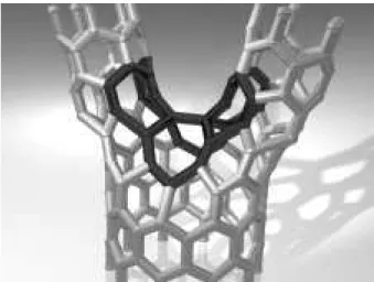
Figure 1. The 6 heptagon topological defect of the Y-junction.
2
Y-Junction
A pure CNT can be uniquely determined by the chiral vector C = na1+ma2, wherenandmare integers anda1 and a2are the graphene sheet lattice vectors, with|ai| ≈2,49
˚
A. The (n, m)CNTs are metallic, if n−m is a multiple of three and semiconducting otherwise, i.e., the armchair CNTs(n, n)are always metallic whereas the zigzag CNTs
(n,0)requires annmultiple of 3.
The Y-junction is modeled here joining three arms of zigzag CNTs together maintaining the original chirality. The large zigzag (m,0) CNT bifurcates into two smaller zigzag CNTs, (n,0) and (n,˜ 0), forming an acute angle between the smaller arms, exactly where six heptagons are supposed to be fixed as a topological defect. This YJ is denoted as m → n/n. Fig. 1 illustrates the chosen YJ described˜
here. The defect atoms, forming six heptagons according to the Crespi rule[10], are marked with dark lines. Indepen-dently of the tube diameters composing the YJ, the number of atoms in each cross section, before and after the bifur-cation region is maintained constant, i.e.,n˜ = m−n. If one considers the YJ composed of an infinite nanotube het-erostructure at which a finite tube is attached composed of an ordered sequence oflcarbon rings (control arm), we call it asm→n/n˜l. Actually one may think that the finite arm
acts as an idealized CNT control of varied extension[11]. Other YJ configurations have been recently studied, show-ing the dependence of interference effects on the topological arrangement of the arms[5].
A singleπ-band tight-binding calculation is used to de-scribe the electronic properties of the CNT structures (pure carbon nanotubes, YJs and YJRs). Effects such as σ-π-hybridisation are not included in this one-band scheme. Rather then describing the system in the k-space, we treat the CNT-structures entirely in a real space picture. We follow the Green function formalism and adopt real-space renormalization group techniques [9, 12, 13]. The local density of states (LDOS) per electron is calculated directly from the relation ρi(ω) = −1/πT r(Ima[ ˜Gii(ω)]) where
the dressed Green functions are obtained by solving a set of coupled matricial Dyson equations given by
˜
Gij(ω) = ˜gi(ω)δi,j+ ˜gi(ω)
X
l6=i
VilG˜lj(ω), (1)
withg˜i denoting a matricial renormalized Green function
corresponding to a single CNT ring, written in terms of the undressedgi(ω) = 1/(ω −ǫo). The microscopic atomic
details of the topological defect (heptagons) are taken into account in the theoretical description through hopping en-ergy matricesVil, connecting the neighboring atomic layers
(rings).
Results for the LDOS of an YJ 14 → n/n˜ with three semi-infinite CNTs are shown in Fig. 2, considering differ-ent combinations of arm sizes. A mean calculation is per-formed through all the atomic sites of a single ring, posi-tioned two ring- layered from the defect. One should no-tice that semiconducting combinations of tubes, such as the
14→ 7/7and14 →4/10generate localized states within the energy gap. Combinations involving at least one
metal-lic tube arm, such as 14 → 6/8 and14 → 5/9, leads to the formation of a continuous band population within the gap. Due to the peculiar electronic properties of carbon nan-otubes it is then possible to modulate the electronic response by selectively proposing proper Y-junctions with particular topology.
Figure 2. Local density of states nearEF = 0of symmetric and asymmetric YJs with big leg (14,0). Curves are shifted for better viewing. When one of the legs is metallic, the LDOS nearEF = 0 is non-zero.
The conductance may be written in terms of the dressed Green functions [13] by following the Landauer formalism[14] and the Kubo-Greenwood formula[15]. At the Fermi energy and for zero temperature one has
Γ(ω) =−2e
2
h 2T r X
mnlk
~
RmnVmnGInl+(ω). ~RlkVlkGIkm+(ω),
(2) in whichR~mn =R~m−R~n,R~ being the atomic site
posi-tion,GI+
means the imaginary part of the advanced Green function and the factor 2 is concerned to spin degeneracy. The present conductance calculation corresponds to the lin-ear response of the total current density flowing through one tube into the other two. One should take care in this type of calculation about the role played by the imaginary part added to the energyω +iη. A finiteη defines an uncer-tainty in the energy, which is inversely proportional to an electronic transient-time. By performing calculations with η ≃10−3,10−4
and considering the control arm finite, one gets spurious results for the conductance. In that sense, it is very important to take correctly the limit ofη →0in or-der to determine the localization properties of the electronic wave function.
Results for the conductance of a metallic YJ of type
12 → 6/6L for different values of L (control tube length)
are shown in Fig. 3. In the depicted energy range, where the conductance of a pure metallic CNT equals two units of a conductance quantum2e2/h
cavity, which number depends on its sizes. It is worth notic-ing that for sufficiently long control tubes (see the example of 100 control rings) a small variation in the number of car-riers causes very large percentile changes of the system’s conductance. Otherwise, an interesting result is the pinning of the conductance value at the Fermi energy for all YJs of finite control tube considered (when correctly taken the limit η →0). One clearly see that by varying the tube length one may modulate the conductance respectively (without getting zero-conductance), which rises the possibility of using the YJ as an idealized three-point transistor.
Fig. 3. Conductance vs. Fermi-energy of a symmetric12→6/6
YJ with 1, 5, 10 and 100 (dotted line) rings in the control leg. Energy window is restricted to energies where (12,0) has two con-ductance channels. Note the pinning of the concon-ductance value at EF = 0, marked with an arrow.
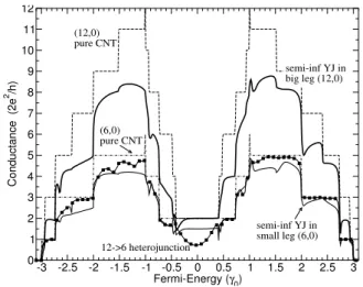
Figure 4. Conductance of symmetric a12→ 6/6YJ with three
semi-infinite legs in comparison with a12 → 6heterojunction.
The conductance channels of a pure(12,0)and(6,0)are shown with dashed lines.
For a single heterojunction of type(12,0)→(6,0), the greatest reduction of the conductance occurs at the center of the electronic band[9], i.e. atEF = 0as shown in Fig. 4.
However, for the12→6/6YJ with three semi-infinite legs, the minimum occurs at the transition of a conductance chan-nel of a pure metallic (12,0) CNT. The conductance of YJs with finite control arm is, like in the case of the heterojunc-tion, limited by the conductance channels of the smaller arm, i.e. six channels in the chosen12 → 6/65YJ. Otherwise, in the case of the semi-infinite YJ the conductance in each of the three semi-infinite legs is restricted by the dimension of their self size: the big(12,0) arm has maximal twelve channels whereas both the two small(6,0)arms have max-imal six. Due to impurity scattering at the defect region, the conductance as a whole is reduced. One may also notice that due to quantum interference phenomena, the sum of the conductance of the small legs does not equal the conduc-tance of the big one (contribution of mixed products of the electronic wave functions of each arm). As expected by the finite value ofηin the calculus, evaluating the semi-infinite limit one may find all the intermediate values on the way to the twelve-channel case. Furthermore, the conductance in the finite leg becomes non-zero for big control lengths, demonstrating the effect of the electronic transient time.
3
Y-Junction Rings
As discussed before, a ring-like nanotube structure may be idealized by joining two Y-Junctions presenting finite arms. Considering twom→nL1/2/n˜L2/2YJs, one may get a Y-Junction-Ring with upper and down arms composed ofL1 andL2rings, respectively. The so-builtm→nL1/˜nL2 → mYJR has two attached semi-infinite arms (m,0) acting as a lead contact, where againn+ ˜n=m.
The easiest way to obtain the annular structure is by cal-culating renormalized non-diagonal Green function, obey-ing the recurrence relation
˜
Gij = G˜iVi,i−1G˜i−1. . .G˜j+1Vj+1,jG˜j, (3)
with G˜i = ¡1−˜giVi,i−1˜gi−1Vi−1,i¢
−1
˜
gi, (4)
fori > jand assumingG˜j= ˜gjin the initial iterative step.
We investigate here the possibility of generating quantum interference phenomena through the annular systems and study its correlation with the arm sizes composing the YJRs. The dependence of the conductance of a (metallic)12→
6L/6L → 12 YJR in the energy window, where a pure
plateau of a pure (12,0) tube, with isolatedδ-functions, in-dicating localized states. One may understand such features setting up a direct correspondence between these intricate carbon system and their one-dimensional counterpart, com-posed of an atomic loop connected to two metallic atomic leads, shown in the inset of the figure.
Figure 5. Conductance (top view) and LDOS (bottom view) of an asymmetric12 →64/6L →12for different values of lower
brace-length (L=6,10,14,18). Inset: Results for a one-dimensional symmetric counterpart, made of one atomic loop with 2 (straight), 4 (dotted) and 6 (dashed) atoms in each brace, connected to two metallic leads.
The LDOS of the 1D ring-system exhibits a sequence of peaks, positioned at energy values quite close to the dis-crete states composing the energy spectra of a single ring - which for the carbon YJR corresponds to a CNT-torus as previously studied[16]. Moreover, just as it happens in the 1D system and in a single YJ, there is a perfect pinning of the LDOS at the Fermi level (EF = 0) for all lengths of ring
braces, provided one considers only even values and sym-metrical brace-tube size.
As YJRs composed of semiconducting tubes do not al-low conductance channels near the Fermi level one should suggest an extra junction formation to overcome this sit-uation. Fig. 6 shows the conductance curves of the semi-conducting YJRs for some brace-lengths, this time connected to metallic leads through (14,0) → (12,0)
heterojunctions[9]. As expected, the conductance and LDOS have finite values and are not zero as in the non-connected case (shown as the dashed curve). Quite sharp peaks are obtained in energy range corresponding to the low band followed by smooth oscillation in the conductance and LDOS results. Here, the brace distributions (size and type) do not drive the main responses; actually it is the metal-lic (12,0) lead which acts as the driving force for all con-figurations. Similar conductance and LDOS oscillatory be-havior, with broken electron-hole symmetry, are also found
for YJR presenting asymmetric brace-tube sizes, such as
12→5L1/7L2→12
Figure 6. Conductance of a14 → 7/7 → 14YJR connected
to metallic lead through(14,0) →(12,0)heterojunctions in the
energy range, where a pure (14,0) has zero- conductance. A pure 14→7/7→14YJR with zero-conductance near the central gap
is shown with dashed lines.
4
Conclusions
We have studied the electronic LDOS and conductance near the Fermi level of single Y-junctions and two-joined YJs, forming a Y-junction ring and compared with one-dimensional counterpart examples. In all situations we ob-served oscillatory behavior depending merely on geometri-cal configuration. In the case of the Y-junction, the control of one of the length-brace can lead to perfect switching be-havior. In the case of the YJR, the position of the leads depending on the annular sites can give rise to complete de-structive or conde-structive quantum interference. Since trans-port phenomena through varied nanotube structures are be-lieved to be promising for technological applications, like a three-point nanotransistor or nanoscale molecular circuit in-cluding a carbon YJR, the understanding of their electronic properties is essential for further development in this field.
Acknowledgments
We would like to thank Drs. M. F. dos Santos for use-ful discussions. This work was partially supported by the Brazilian Agencies CNPq,CAPES, and FAPERJ.
References
[1] C. Papadopoulos, A. Rakitin, J. Li, A.S. Vedeneev and J.M. Xu, Phys. Rev. Lett.85, 3476 (2000).
[2] M. Terrones, F. Banhart, N. Grobert, J.-C. Charlier, H. Ter-rones and P.M. Ajayan, Phys. Rev. Lett.89, 75505 (2002).
[4] L.P. Bir´o, R. Ehlich, Z. Osv´ath, A. Ko´os, Z.E. Horv´ath, J. Gyulai, J.B. Nagy; Diamond and Related Materials11, 1081 (2002).
[5] A. Andriotis, M. Menon, D. Srivastava and L. Chernozaton-skii; Phys. Rev. B65, 165416 (2002).
[6] H. Watanabe, C. Manabe, T. Shigematsu and M. Shimizu, Appl. Phys. Lett.78, 2928 (2002).
[7] G. Cuniberti, J. Yi and M. Porto, Appl. Phys. Lett.81, 850 (2002).
[8] L. A. Chernozatonskii, Phys. Lett. A172, 173 (1992). [9] M. S. Ferreira, T. G. Dargam, R. B. Muniz and A. Latg´e,
Phys. Rev B62, 16040 (2000).
[10] V. H. Crespi, Phys. REv. B58,12671 (1998).
[11] G. Treboux, P. Lapstun, Z. Wu, and K. Silverbrook, J. Phys. Chem. B103, 8671 (1999).
[12] M. S. Ferreira, T. G. Dargam, R.B. Muniz and A. Latg´e, Phys. Rev B63, 245111 (2001)
[13] A. Latg´e, D. C. Marcucci e M. V. Tovar Costa, Physica E13, 1264 (2002); C. G. Rocha, T. G. Dargam, and A. Latg´e, Phys Rev. B65165431, (2002).
[14] J. Mathon, M. Villeret, and H. Itoh, Phys. Rev. B52, R6983 (1995).
[15] R. Kubo, J. Phys. Soc. Jpn,12, 570 (1957).