X-ray Scattering from Self-Assembled InAs Islands
A. Malachias
∗, B. R. A. Neves
∗, W. N. Rodrigues
∗, M. V. B. Moreira
∗, S. Kycia
†,
T. H. Metzger
#, and R. Magalh˜aes-Paniago
∗† ∗Departamento de F´ısica, Universidade Federal de Minas Gerais, Instituto de Ciˆencias Exatas
Campus da Pampulha, Caixa Postal 702, 30123-970 Belo Horizonte, Minas Gerais, Brazil #
European Synchrotron Radiation Facility, BP 220, F-38043 Grenoble Cedex, France
†
Laborat´orio Nacional de Luz S´ıncrotron, Caixa Postal 6192, 13084-971, Campinas, S ˜ao Paulo, Brazil
Received on 31 March, 2003
In this work several structural and chemical properties of self-assembled InAs islands grown on GaAs(001) are studied using surface x-ray scattering with synchrotron radiation. The technique of x-ray diffraction under grazing incidence condition was employed to differentiate coherent and incoherent islands. We used a model of a strained pyramidal island to interpret the x-ray results and correlate size and strain-state of these islands. The degree of GaAs interdiffusion in the islands was inferred from the variation of volume of the unit cell. The Poisson’s ratio of the two materials involved establishes a limit of tetragonal distortion for this material. Any variation in this distortion is associated with the presence of Ga inside the islands.
1
Introduction
The electronic properties of self-assembled islands, such as InAs grown on GaAs(001) are extremely dependent on their inner strain and chemical state. Although a large num-ber of variables rules island formation only a few features of their final state determines their technological applica-bility: a) absence of defects like dislocations or stacking faults, directly related to quantum efficiency of quantum dots (QDs); b) morphological homogeneity, which gives op-tical and electronic response quality and; c) elastic strain and intermixing. Here we employ x-ray scattering to study features (a) and (c), described in two different parts of this work. Firstly we show how x-ray scattering provides accu-rate quantitative information about the coexistence of coher-ent and incohercoher-ent InAs islands grown in GaAs(001). Sec-ondly a reciprocal space map enables to observe the three-dimensional strain status and infer the chemical composition of InAs nanostructures.
2
InAs coherent-incoherent
transi-tion
Growing dislocation-free nanostructures with a narrow size distribution is crucial for the optimal performance of op-toeletronics quantum-dot devices. Since early work in this field, the transition of InAs dots from coherent to incoherent states has been mostly investigated by Atomic Force Mi-croscopy (AFM) [1]. Samples with coherent and incoher-ent quantum dots usually exhibit a bimodal size distribution, where coherent (strained) islands are smaller than incoher-ent (relaxed) nanostructures [1]. However, the exact point of
the coherence-incoherence transition is hard to be identified by AFM, since at this point, islands of both types may have nearly the same size. X-ray scattering is used in this paper to separate coherent and incoherent islands by relating their size to strain-state.
The heteroepitaxial growth of InAs on GaAs(001) usu-ally proceeds as follows [1]: while the amount of deposited InAs is less than∼1.6 monolayers (MLs), a 2-dimensional layer can be grown. Increasing this coverage beyond 1.6 MLs up to∼2.3 MLs, coherently strained (dislocation-free) dots are formed. For higher coverages, dislocations start to appear, generating relaxed islands on the surface [1].
For this work, three InAs/GaAs samples were grown by molecular beam epitaxy on a GaAs(001) substrate. In sam-ple A, 1.9 MLs of InAs were deposited on a GaAs buffer layer at 500 ˚ C at a rate of 0.16 ML/s and As4pressure of 5.8×10⁻⁵
Torr. In sample B, these same steps were adopted and, subsequently, a 30ML GaAs spacer was deposited on the InAs dots, followed by 1.9 MLs of InAs, forming an InAs/GaAs/InAs bilayer. In sample C 3.0 MLs of InAs is-lands were deposited at 535 ˚ C. AFM measurements con-firmed the formation of self-assembled dots.
in-dependent circle and the exit angleαf was measured from 0 ˚ to 1 ˚ by a position sensitive detector (PSD). Samples A and B (sample C) were (was) illuminated at a grazing an-gle αi = 0.25 ˚ (αi = 0.3 ˚ ) with an x-ray beam of wave-lengthλ= 1.560 ˚A (λ= 1.378 ˚A). The X-ray scattering was measured as a function of qradial= qr = (4π/λ) sin(2θ/2), which is strain-sensitive, and also of qangular = qa=(4π/λ) sin(2θ/2) sin(2θ/2-ω), which is size sensitive, integrating qz = (2π/λ) [sin(αi) + sin(αf)] from 0.02 ˚A−1 to 0.07 ˚A−1 [2]. In grazing incidence geometry, the scattering is due to atomic planes perpendicular to the sample surface and, es-sentially, two types of scans can be done. A radial scan is performed couplingω to 2θ, spanning from InAs to GaAs Bragg peaks in reciprocal space. Thus, by Bragg’s law (λ= 2d sin(2θ/2)), this radial scan is sensitive to the strain of the sample. Angular scans are performed solely byω(qa), with 2θ(qr)fixed. These scans are size sensitive, since the size of the region can be inferred from the width of the qa-scan profile [3]. Fig. 1(b) shows a scheme of grazing incidence geometry.
ω
2θ
(a)
PSD
(b)
α
iα
fα
i2
θ
ω
q
q
zq
aq
rPSD
Figure 1. (a) X-ray scattering setup at XD1 beamline (LNLS). (b) Grazing incidence diffraction geometry.
Figure 2 shows two radial scans along the (2 2 0) direc-tion taken from samples A and C. Both samples present a reasonable amount of scattered x-ray intensity between the
InAs and GaAs bulk peak positions. This is a clear evi-dence of the existence of a lattice parameter gradient inside the dots from the bottom to the top of the islands [2]. Be-sides the contribution from coherent dots, sample C shows some extra diffracted intensity near the InAs bulk peak posi-tion. Considering that this sample contains almost twice the amount of InAs than sample A and that islands with this cov-erage have already crossed the coherence-incoherence tran-sition [1], we infer that this sample contains relaxed QDs with the lattice parameter of bulk InAs (6.06 ˚A).
2.85 2.90 2.95 3.00 3.05 3.10 3.15 3.20 102
103 104 105 106 107
GaAs Substrate reflection
InAs Strained dots
InAs Relaxed dots
A - Coherent dots (1.9ML) C - Partially incoherent dots (3.0ML)
In
te
nsi
ty
(
a
bsol
ut
e count
s)
qradial(Å-1)
Figure 2. Radial scans for samples A and C. The two gaussians drawn for sample C to indicate the contributions of relaxed and strained islands.
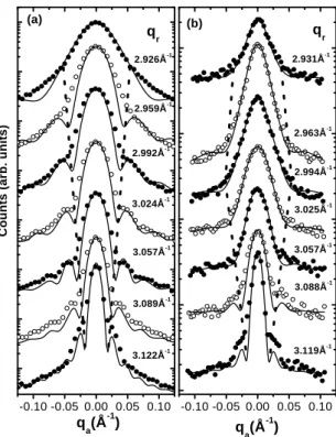
-0.10 -0.05 0.00 0.05 0.10 -0.10 -0.05 0.00 0.05 0.10 q r qr 2.926Å-1 2.959Å-1 2.992Å-1 3.024Å-1 3.057Å-1 3.089Å-1 3.122Å-1 (a) C ount s ( a rb. uni ts )
qa(Å-1) q
a(Å -1 ) 3.119Å-1 3.088Å-1 3.057Å-1 3.025Å-1 2.994Å-1 2.963Å-1 2.931Å-1 (b)
Figure 3. Angular scans at different radial (qr)positions for (a)
sample A and (b) sample. Solid lines are fits according to eq.1. Dashed lines were drawn to indicate the approximate width of each angular scan.
Based on AFM measurements of all samples, the islands have a pyramidal shape with a square section of side length L along the [1-10] direction and a varying local lateral lattice parameter. In this case, the scattered intensity of an angular qa-scan for a fixed qrand qzcan be calculated using [3]
I(qa, qr, qz)∝ ¯ ¯ ¯ ¯ ¯ ¯ M X j=1
eiLjqa−1
qa
·e
iNjdjqr−1
eidjqr−1 e
iqzhj
¯ ¯ ¯ ¯ ¯ ¯ 2 (1) where M is the number of square sections parallel to the sur-face,Lj, djandhjare the length, the lattice parameter and the height of square section j, respectively. Nj ≡Lj/dj is the number of atomic lines at plane j. The solid lines in Figs. 3 (a) and (b) are least-square fits done using eq.1, which were performed adjusting the square side length L for every fixed qr(corresponding to a small region of the island of lattice parameter d = 2π/qr).
A plot of the island side lengthLas a function of lattice parameterdis shown in Fig. 4. Sample A (coherent QDs) presents a linear decrease of the side length as a function of lattice parameter as reported before [2]. Samples B and C, besides the contribution from coherent islands (close to GaAs value), also exhibit larger side lengths close to InAs value, which are, therefore, assigned to be relaxed islands (and correspond to an average value of the size of these is-lands, not a local lattice parameter). An unambiguous dif-ferentiation regarding size between coherent and incoherent islands was therefore obtained with this x-ray technique.
5.65 5.70 5.75 5.80 5.85 5.90 5.95 6.00 6.05 6.10 0 50 100 150 200 250 300
Average island length Local island length
InAs GaAs
A 1.9 ML InAs B 2 x 1.9 ML C 3.0 ML
L Si de l e ngt h ( Å )
Lattice Parameter (Å)
Figure 4. Islands side length as a function of lattice parameter for all samples. The straight lines are linear fits for coherent islands.
The linear fits done to points associated to coherent is-lands were in the format L(∆d) = L0- D∆d, where L0is the island bottom size (in ˚A), D is a fitting parameter and∆d is the deviation from the GaAs lattice parameter ( ˚A). We ob-tained L = 280 ˚A – 130·∆d, L = 120 ˚A – 100·∆d and L = 270 ˚A - 170·∆d, for samples A, B and C, respectively.
50 100 150 200 250 300 350
0 5 10 15 20 25 Count s ( % )
L - Side length (Å) InAs coverage
A - 1.9 ML B - 2 x 1.9 ML C - 3.0 ML
Figure 5. Size distribution graphs of all samples obtained from analysis of AFM images.
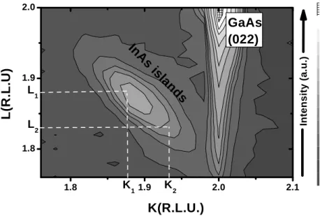
1.8 1.9 2.0 2.1 1.8
1.9 2.0
L
2
L
1
K2
K1
GaAs
(022)
In
As i
slands
In
te
n
s
ity (a
.u
.)
K(R.L.U.)
L(
R.
L.
U)
Figure 6. X-ray reciprocal space map of InAs/GaAs (001) islands near the (022) GaAs reflection. K and L reciprocal lattice units refer to the lattice of bulk GaAs. This scan allows us to associate horizontal and vertical lattice parameters, as represented by dashed lines for two pairs of valuesK1,L1and K2,L2.
3
Ga interdiffusion inside InAs dots
X-ray reciprocal space mapping has already been used to study self-assembled islands, mainly using strain models to reproduce the intensity maps [4,5]. Here grazing inci-dence diffraction was used in combination with x-ray re-ciprocal space mapping to infer the three-dimensional strain and chemical status of InGaAs islands. With this informa-tion the tetragonal distorinforma-tion of all unit cells inside the is-lands was quantified. The interdiffusion profile was then de-duced from the elastic distortion of the unit cell determined by the Poisson ratio of the InGaAs alloy.
Following the GID measurements, x-ray reciprocal space mapping (in fixed incident angle mode) near the sub-strate GaAs (022) reflection was performed for sample C. The scattering measurements were performed at the XD2 beamline at the Brazilian Synchrotron Light Source (Lab-orat´orio Nacional de Luz S´ıncrotron), in Campinas, Brazil. This beamline is equipped with a double bounce sagitally focussed Si(111) monochromator and a standard 4-circle diffractometer. The incidence angleαi was set to 0.10 to maximize the islands/substrate signal ratio. The x-ray map-ping was measured by a point scintillation detector.
Figure 6 shows the reciprocal space intensity map of the x-ray scattering stemming from sample C. This rectangu-lar reciprocal space map scan starts near the position of the relaxed (022) InAs reflection and goes up to the position of the (022) GaAs substrate peak, spanning from K = L = 1.76 R.L.U. until K = 2.10 R.L.U and L = 2.0 R.L.U.. Two main contributions can be qualitatively identified. First, we clearly observe the crystal truncation rod along the 001 di-rection crossing the (022) GaAs peak, parallel to the GaAs surface normal. We also observe the island scattering in-tensity distribution, which already shows the signature of the tetragonal distortion of the island lattice. The lateral
(in-plane) compression of the InAs island lattice by the substrate leads to a vertical (out-of-plane) expansion. In reciprocal space this can be seen from the x-ray map, where for larger K the main intensity is seen for smaller L.
In order to start a quantitative analysis of fig.6, a few as-sumptions were made. First, each portion of the islands at height z with respect to the substrate has a horizontal lat-tice parameter. This layer is constrained by a biaxial strain that creates a tetragonal distortion in the islands unit cells, changing the out-of-plane lattice parameter. Finally, there is a direct correlation between horizontal and vertical lattice parameters. These approximations are valid assuming that the island behaviour is similar to the bulk, meaning that it has the same elastic constants.
The measurement of Fig. 6 allowed us to correlate the in-plane and out-of-in-plane lattice parameters. This association was obtained as follows: for each L scan for K fixed, an in-plane lattice parametera//=aGaAs * 2/K was associated. The peak position of each L scan (determined from a gaus-sian fit) was associated to the out-of-plane lattice parameter
a⊥=aGaAs* 2/Lpeak. In this way, pairs of values of (a//,
a⊥), obtained from(K, Lpeak)pairs, were obtained. The left plot of Fig. 7 shows values of (a//, a⊥)related to
5.7 5.8 5.9 6.0 6.1 6.0
6.1 6.2 6.3
205 210 215 220
a ⊥
(Å
)
a
// (Å)
U
n
it c
e
ll v
o
lu
m
e
(Å
3 )
Figure 7. Left: correlation between in-plane and out-of-plane lat-tice parameters in InAs islands. Right: unit cell volume as a func-tion of horizontal lattice parameter. The error bars are smaller than the symbol sizes.
x= alocal−aIn/As
aGaAs−aInAs
(2)
One can calculate the unit cell volume from pairs of val-ues (a//, a⊥), considering that the unit cell is tetragonal,
i.e.,V = a2
// a⊥. The right plot of Fig. 7 shows the unit
cell volume as a function of in-plane lattice parameter. This result shows that the unit cell volume diminishes as the in-plane lattice parameter decreases. This is a first indication of the presence of Ga inside the islands. However, one must consider the effect of strain imposed by the substrate.
A more realistic approximation of the behaviour of this system can be obtained using the elastic properties of InAs and GaAs. The in-plane and out of plane strain components are defined as:
ε//= 2
a//−alocal
a//+alocal
and ε⊥= 2
a⊥−alocal
a⊥+alocal
. (4)
The relationship between vertical and horizontal strain com-ponents depends on the type of compression (axial or bi-axial) the material is subjected to.
For a biaxial compression the strain components are re-lated by [6]:
ε⊥=
−2ν
1ν ǫ//. (5)
Insertingε⊥andε// (equation 4) into eq. 5,alocal can be found solving the equation:
⌋
(alocal)
2
(1 +ν) +alocal(1−3ν)(a⊥−a//) +a⊥alocal(1 +ν) = 0. (6)
This quadratic equation has the following solutions
alocal=
(3ν−1)(a⊥−a//)±p(1−3ν)2(a⊥−a//)2+ 4(1 +ν)2a⊥a//
−2(1 +ν) , (7)
⌈
where one of the solutions leads to a negative lattice param-eter. From the positive value of alocal and eq. 2, the Ga concentration could be estimated.
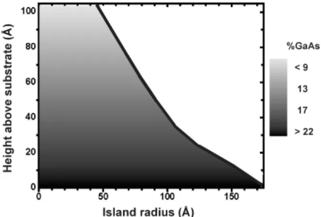
Figure 8. Ga content map in InAs:GaAs(001) islands determined using the method described in the text.
The InAs and GaAs Poisson ratios are 0.35 and 0.31, respectively. A self-consistent procedure to calculatealocal
(eq. 7) was adopted: first the InAs Poisson ratio was used to obtain an initial estimate for the Ga concentration. A cor-rected value for the Poisson ratio was obtained from Veg-ard’s law and the Ga concentration:
νalloy =x· νGaAs+ (1−x)· νInAs.
This new Poisson ratio was taken again to eq. 7 and new values foralocalandxwere found. The result of this calcu-lation can be seen in Fig. 8.
The interpretation of the plot of Fig. 8 is straightfor-ward. For regions close to substrate, where the horizontal lattice parameter is near GaAs value the Ga concentration is higher (∼25%). Closer to the island top, the presence of Ga is smaller. This result is probably due to kinetic limited Ga interdiffusion during the deposition of InAs.
4
Conclusion
shown that the x-ray scattering technique clearly separates these two island types even when coherent and incoherent QDs have about the same size. We have also used recip-rocal space mapping under grazing incidence geometry to study the local tetragonal distortion of InAs islands grown on GaAs(001). For the case of sample C we observed a variation of Ga content from 25% (base of the island) up to 8% (top of the islands). This method is in principle ca-pable of determining the complete three-dimensional strain and chemical status of any island-substrate system.
Acknowledgement
The authors acknowledge support from PRONEX, FAPEMIG, CNPq and LNLS (ABTLus).
References
[1] D. Leonard, K. Pond, P.M. Petroff, Phys. Rev. B 50, 11687 (1994).
[2] I. Kegel, T. H. Metzger, J. Peisl, A. Lorke, J. M. Garcia, P. M. Petroff, Europhys. Lett. 45, 222 (1999); I. Kegel, T. H. Metzger, A. Lorke, J. Peisl, J. Stangl, G. Bauer, P. M. Petroff, Phys. Rev. B, 63, 35318 (2001)
[3] J.M. Cowley, Diffraction Physics, Ed. North-Holland, (1981).
[4] K. Zhang, Ch. Heyn, W. Hansen, Th Schmidt, and J. Falta, Appl. Phys. Lett. 77, 1295 (2000).
[5] J. Stangl, A. Daniel, V. Holy, T. Roch, G. Bauer, I. Kegel, T. H. Metzger, O. G. Schmidt, and K. Eberl, Appl. Phys. Lett. 79, 1474 (2001).
[6] See, e.g., J.Y. Tsao, Materials Fundamentals of Molecular