Brazilian Journal of Physics, vol. 36, no. 2A, June, 2006 365
Limitation of Electron Mobility in Modulation-Doped In
0
.
53
Ga
0
.
47
As/InP
Quantum Wells at Low Temperatures
F. M. S. Lima, A. B. Veloso, A. L. A. Fonseca, and O. A. C. Nunes Instituto de F´ısica, Universidade de Bras´ılia, P.O. Box 04455, 70919-970 Bras´ılia-DF, Brazil
Received on 4 April, 2005
The low-temperature electron mobility is investigated here for electrons confined in modulation-doped In0.53Ga0.47As/InP single symmetric quantum wells. The subband structure calculation is developed via
varia-tional method, both Schr¨odinger and Poisson equations being solved simultaneously with adequate heterointer-face matching conditions. With this in hands, the main electron scattering rates are computed, namely alloy dis-order, remote ionized impurity, and interface roughness. As a result, interesting interchanges in these scattering rates were found by varying the well width and the spacer width, which show that some scattering mechanisms can surpass the alloy disorder scattering rate and come to limit the electron mobility, a behavior not reported in the literature.
Keywords: Electron mobility; In0.53Ga0.47As/InP Quantum Wells; Low-temperature
I. INTRODUCTION
The evolution of epitaxial growth techniques for III-V semiconductor heterostructures has allowed an excellent con-trol on both composition and doping, furnishing high-quality samples with almost abrupt heterointerfaces and doping pro-files, which are crucial for the fabrication of modern electronic and optoelectronic devices [1]. It is well-known that the high-est electron mobility in semiconductor heterostructures has al-ways been observed in GaAs/AlGaAs quantum heterostruc-tures [2], but n-doped AlGaAs carrier supply layers has some inconveniences for high-speed device applications, e.g., deep levels, interface states, and gate leakage [3]. These unwanted effects have been overcome by growing heterostructures with binary compounds in the barriers, the choice of the com-pounds being decisive for the device performance. In this context, In0.53Ga0.47As/InP modulation-doped quantum wells (QWs) has been a focus of interest due to the absence of strain effects (lattice-matched heterostructure) and also due to the negligible concentrations of DX centers and dislocations on InP barrier layers [4]. Indeed, as compared to In0.52Al0.48As, another important alloy that lattice-matches to In0.53Ga0.47As, the InP supply layers present a larger Γ-L separation (630 meV in comparison to 340 meV), which reduces the proba-bility of activation of DX-like centers and also lowers the hot carriers transfer between the channel and the doped layers [5]. However, the search for high carrier mobility in InGaAs/InP heterostructures has come up against the alloy disorder (AL-LOY) scattering of electrons in the InGaAs channel, which has always been considered as the main scattering mechanism. Since electron mobility is the physical quantity that de-termines the speed of electronic devices and alloy disorder is an important scattering mechanism in In0.53Ga0.47As/InP modulation-doped QWs, we decided to investigate here in this work the possibility of other scattering mechanisms limit the mobility in such heterostructure. We considered interface roughness (IR) scattering, due to its importance in the domi-nance of electron mobility in thin GaAs/AlGaAs QWs [6,7], and remote ionized impurity (II) scattering, since it limits the mobility in modulation-doped QW samples with thin enough
spacer layers.
II. MODEL
As convenient approximations to the subband structure cal-culation in In0.53Ga0.47As/InP lattice-matched QWs we have taken into account the effective mass approximation, with Γ electrons moving in an isotropic, parabolic conduction band (CB). We consider a single symmetric QW, i.e., an In0.53Ga0.47As channel sandwiched by InP barrier layers. The QW channel has width L and the InP barriers are doped with donors, except in the undoped spacer layers, whose width is LS, which are essential for obtaining high-mobility in doped heterostructures [8]. The band-offset at the CB is V0and the doping concentration is ND, the donor binding energy being ED(see Ref. [9]). Since both the electron effective mass m∗(z) and the dielectric constantε(z)change along the growth direc-tion (z-axis) special forms for the Hamiltonian and the Poisson equation should be considered [9]. In this way, the coupled Schr¨odinger and Poisson equations read, respectively,
· −~
2
2 ∂ ∂z
1 m∗(z)
∂ ∂z+V(z)
¸
χj(z) =Ejχj(z) (1)
and
∂ ∂zε(z)
∂
∂zVH(z) = e2
ε0
£
ND+(z)−NA−(z)−n(z)¤
. (2)
366 F.M.S. Lima et al.
besides the wavenumber k referent to the in-plane wavevector
k=kxˆi+kyˆj. The charge concentrations on the right-hand side of Eq. (2) are ND+(z)for ionized donors, NA−(z)for ion-ized acceptors, and n(z) =Ns|χ(z)|2for quasi-2D electrons in the quantum limit, Nsbeing the electron gas sheet density. This density depends on both the absolute temperature T and the Fermi energy EFaccording to (see, e.g., Ref. [11] )
Ns= m∗
π~2kBT ln
©
1+exp£(EF−E0)
±
kBT
¤ª
. (3)
It is important to note that Eq. (2) was solved within the depletion approximation [9], the presence of ionized residual acceptors being neglected since it has only small effects on the charge transfer [12]. Taking this approximation into ac-count, the charge conservation equation simplifies to LD= Ns±(2ND), with LD being the width of the depletion layer (where all impurities are treated as being ionized).
The use of Eqs. (1) and (2) requires unusual matching con-ditions for the derivatives ofχ(z)and VH(z)[9]. Taking the centre of the well at z = 0, the heterointerfaces will be located at z=±ℓ,ℓ≡L±2. For the interface at z= +ℓwe have
1 m∗A
∂χ ∂z
¯ ¯ ¯ ¯ℓ−
= 1
m∗B
∂χ ∂z
¯ ¯ ¯ ¯ℓ+
(4)
and
εA
∂VH
∂z
¯ ¯ ¯ ¯ℓ−
=εB
∂VH
∂z
¯ ¯ ¯ ¯ℓ+
. (5)
The index A (B)refers to the channel (barrier) material. In seeking for a variational scheme more accurate and flex-ible than the previous ones [9,12-15], we included a 2nd-degree term in the part of the variational wavefunction for −ℓ <z<+ℓ(i.e., into the InGaAs channel), as given by
χ(z) =Bpkw
¡
1+c z2¢cos(kwz). (6) For the envelope wavefunction in the barrier regions we kept the usual form, namely, A√a exp£
±a 2(z±ℓ)
¤
, the upper (lower) signs being for z<−ℓ(z>+ℓ).
Choosing the Fermi level as the zero energy reference level, the variational method follows by deriving an analytic expres-sion to the integral corresponding to the quantum mechanical expectation valueˆ
H® =ˆ
T+V(z)®
in terms of the varia-tional parameters. The minimization ofhHi=hHi(kw,c; Ns) was obtained by solving the 3×3 non-linear system composed by Eq. (3), with EF = 0, and the equations ∂∂k
whHi=0 and
∂
∂chHi=0. The numerical solution was found via Broy-den’s method, which is an interesting alternative to Newton’s method since it is less sensitive to the initial guess and spends less running time [16].
The main scattering rates for electrons confined in In-GaAs/InP heterostructures at low temperatures are well-known [8,17]. With respect to phonons, for T <100 K the
population of optical phonons is negligible and for T<60 K acoustic phonons scattering contributes little to the mobility limitation [8]. By considering the electrons in the quantum limit, higher subbands are not populated and there is no in-tersubband scattering. The background impurity (BI) scatter-ing is more complex to be calculated and will not be included here, therefore our results may not be valid for samples with residual acceptor concentrations above, say, 3 x 1015 cm−3 [18], a situation that is rarely found in samples grown by mod-ern epitaxial techniques [2]. Thus we will concentrate only on ALLOY, IR, and remote II scattering mechanisms.
Since the carrier scattering is efficiently screened by the electron gas, the screening effect was taken into account in the lines of Ref. [19]. This effect was neglected in our ALLOY scattering rate calculation because it is essentially a short-range scattering mechanism [12].
The ALLOY scattering rate was calculated following the usual model found in literature [7,8,11], namely,
1 τALLOY
= m∗A
π~3x(1−x)ΩV 2Z +ℓ
−ℓ
dz|χ(z)|4. (7) Note that the alloy is into the channel in InxGa1−xAs/InP heterostructures. The alloy scattering parameters are defined elsewhere [11].
The IR scattering rate reads
1 τIR(k)=
m∗A∆2Λ2 2~3 [h(ℓ)]
2R2π
0 dα (1−cosα)
×h 1 ε(q)2 exp
³ −Λ24q2
´i
q=2k sin(α2)
, (8)
where h(ℓ)is an auxiliary function defined in Ref. [11], as well as∆andΛ. In this equation, k is the electron wavenum-ber andαis the scattering angle.
The remote II scattering rate is given by [11]:
1 τII(k)
= 4π~
m∗Aa∗B2ND
Zπ
0
dα(1−cosα)F(α,k), (9)
where aB∗is the effective Bohr radius. The auxiliary function in the integral is:
F(α,k)≡[q×ε(q)]−2×
Z
dzi[gimp(q,zi)]2, (10) where q=2 k sin¡α±2¢(quasi-elastic scattering approxima-tion). The integral over zi, the impurity position covers both depletion layers and gimp(q, zi)is the form factor defined in Ref. [11].
Both the IR and II scattering times depend on k and their av-erages were calculated within the independent scattering ap-proximation by doing
hτi(E)i=
Z
τi(E)E
∂f
∂EdE
ÁZ
E∂f
Brazilian Journal of Physics, vol. 36, no. 2A, June, 2006 367
where the index i refers to each scattering process, E =
~2k2±
(2 m∗) is the carrier kinetic energy, and f(E) is the Fermi-Dirac distribution. The partial mobilities are µi =
e
m∗ hτiiand the total mobility µ is computed via Matthiessen’s rule, i.e., 1±
µ=∑
i 1±
µi.
III. RESULTS AND DISCUSSIONS
The variational scheme described above was implemented in MAPLE V mathematical software due to its symbolic facil-ities. We computed the electron subband structure and mobil-ity for a typical example of n-doped In0.53Ga0.47As/InP sym-metric QW [9]. The relevant parameters are: L= 100 ˚A, LS= 150 ˚A, V0= 264.9 meV, ND=2×1018cm−3, ED= 50 meV, and T = 4.2 K. For InxGa1−xAs we used m∗A(x)andεA(x)as given in Ref. [20], with x = 0.53. For the InP barriers we used m∗B= 0.077 m0andεB= 12.35 [9]. We found Ns=9.62×1011 cm−2 for the QW example identified above, in good agree-ment to the usual (less accurate) variational scheme, in which Ns∼=9.4×1011cm−2[9].
The parameters related to ALLOY scattering are the InxGa1−xAs lattice parameter a0(x) =5.65325+0.40515x (in
˚
A) [20], which is used to compute Ω=a0(x)3
.
4, and V = 650 meV [21]. For the IR scattering we choose∆=2.5 ˚A andΛ= 120 ˚A [22]. Taking these parameters into account, we found µALLOY=9.16×104cm2/ Vs, µIR=4.55×105cm2/Vs, and µII=7.51×105cm2/Vs. This furnishes a total mobility of 6.92×104 cm2/Vs. According to Ramvall et al. [17], a BI partial mobility of 5×106cm2/Vs is expected, due to the presence of ionized residual acceptors. This is two orders of magnitude larger than µALLOY, which allowed us to neglect this scattering mechanism.
The dependencies of the partials and total mobilities on the well width are depicted in Fig. 1, below, for a fixed spacer thickness of 150 ˚A. Note that, the IR partial mobility curve crosses the ALLOY curve for L∼= 59 ˚A. Note that the IR scattering dominates entirely the total mobility behavior for smaller well widths. At the crossing point, the total mobility is 3.2×104cm2/Vs. As the II curve is one order of magnitude above the ALLOY curve, it practically does not contribute to the total mobility.
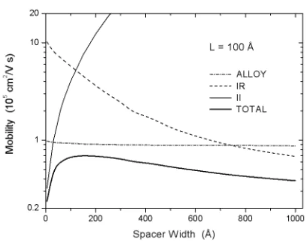
The mobility dependence on the spacer thickness is de-picted in Fig. 2, for a fixed well width of 100 ˚A. Clearly, for LS above, say, 750 ˚A the IR scattering rate overcome the ALLOY one. Note that the curve for IR partial mobility decreases with LS due to the increase of the h(ℓ) auxiliary function, which enhances the IR scattering rate as seen in Eq. (8). For spacer thicknesses smaller than, say, 200 ˚A the rapid decrease of the II partial mobility affects the total mobility, which otherwise would increase, accompanying the ALLOY curve. In this range of spacers, the II scattering increases and leads to the formation of a maximum at LS= 155 ˚A, where the mobility is 6.9×104cm2/Vs.
As seen at the left of Fig. 2, the rapid decrease of the curve for II partial mobility makes it smaller than the ALLOY one for LSbelow, say, 30 ˚A. Unfortunately, for such small values
FIG. 1: Dependencies of partials and total mobilities on the well width for an InGaAs/InP symmetric QW with LS = 150 ˚A. The IR and ALLOY curves cross for a well width of 59 ˚A. For smaller widths the IR partial mobility decreases rapid and it becomes the dominant scattering mechanism. At the crossing point, the total mobility is 3.2×104cm2/Vs.
FIG. 2: Mobility dependence on the spacer thickness for a 100 ˚ A-wide InGaAs/InP symmetric QW. Note that the IR curve intercepts the ALLOY curve at LS∼750 ˚A. The rapid decrease of the II partial mobility for LSbelow 200 ˚A clearly affects the total mobility, which has a maximum at LS= 155 ˚A.
368 F.M.S. Lima et al.
IV. CONCLUSION
In this work, the mobility was calculated for quasi-2D elec-trons in In0.53Ga0.47As/InP single symmetric QWs. Some in-teresting interchanges in the low-temperature electron mobil-ity dominance were found. To the authors knowledge, there is no indicative of such interchanges in the literature and it may be due to the belief that the ALLOY scattering always domi-nates the mobility in heterostructures whose channel is an al-loy, as in InGaAs/InP QWs. Since these predictions should
be at least qualitatively measurable, experimental results are awaited.
Acknowledgement
A.L.A.F. and O.A.C.N. wish to thank the CNPq (Brazil-ian agency) for the Doctor Research Grants during the course of this work. Thanks are also due to FINATEC (Brazilian agency).
[1] See, for example, V. V. Mitin, V. A. Kochelap, and M. A. Stroscio. Quantum Heterostructures. Cambridge Univ. Press, Cambridge MA, 1999.
[2] C. T. Foxon, J. Cryst. Growth 251, 1 (2003).
[3] K. Radhakrishnan et al., J. Vac. Sci. Technol. A18, 713 (2000). [4] M. J. Kelly, Low-Dimensional Semiconductors: Materials,
Physics, Technology, Devices. Oxford U. P., New York, 1995.
[5] M. Kusters, A. Kohl, S. Brittney, T. Funke, V. Sommer, K. Heine. InP and Related Materials, 1993, p.473.
[6] K. Hirakawa, T. Noda, and H. Sakaki, Surf. Sci. 196, 365 (1988).
[7] A. Gold, Z. Phys. B – Cond. Matter 74, 53 (1989).
[8] C. Weisbuch and B. Vinter. Quantum Semiconductor
Struc-tures. Acad. Press, Orsay (France), 1991.
[9] F. M. S. Lima, L. C. Lapas, and P. C. Morais, Physica E 16, 190 (2003).
[10] P. Ruden and G. H. D¨ohler, Phys. Rev. B 27, 3538 (1983). [11] F. M. S. Lima, A. L. A. Fonseca, O. A. C. Nunes, and Q.
Fanyao, J. Appl. Phys. 92, 5296 (2002).
[12] J. A. Brum and G. Bastard, Solid State Commun. 53, 727
(1985).
[13] S. B. Ogale and A. Madhukar, J. Appl. Phys. 56, 368 (1984). [14] P. K. Basu and D. Raychaudhury, J. Appl. Phys. 68, 1 (1990). [15] K. Suresha, S. S. Kubakaddi, and B. G. Mulimani, Physica E
21, 143 (2004).
[16] J. E. Dennis and R. B. Schnabel, Numerical Methods for
Unconstrained Optimization and Nonlinear Equations. SIAM
Class. Appl. Math. 16, Philadelphia (USA), 1996. [17] P. Ramvall et al., J. Appl. Phys. 84, 2112 (1998).
[18] F. M. S. Lima, A. L. A. Fonseca, O. A. C. Nunes, Fanyao Qu, V. N. Freire, and E. F. da Silva Jr., Physica E 17, 322 (2003). [19] F. M. S. Lima, Qu Fanyao, O. A. C. Nunes, and A. L. A.
Fon-seca, Phys. Stat. Sol. (b) 225, 43 (2001).
[20] D. Vasileska, C. Prasad, H.H.Wieder, and D. K. Ferry, J. Appl. Phys. 93, 3359 (2003).
[21] A. Kabasi and D. Chattopadhyay, Solid State Commun. 69, 297 (1989).